Mechanism of Synergistic Effects of Neutron- and Gamma-Ray-Radiated PNP Bipolar Transistors
Abstract
The synergistic effects of neutron and gamma ray radiated PNP transistors are systematically investigated as functions of the neutron fluence, gamma ray dose, and dose rate. We find that the damages show a ‘tick’-like dependence on the gamma ray dose after the samples are radiated by neutrons. Two negative synergistic effects are derived, both of which have similar magnitudes as the ionization damage (ID) itself. The first one depends linearly on the gamma ray dose, whose slope depends quadratically on the initial displacement damage (DD) and can be attributed to the healing of neutron-radiation-induced defects in silicon. The second one has an exponential decay with the gamma ray dose, whose amplitude shows a rather strong enhanced low-dose-rate sensitivity (ELDRS) effect and can be attributed to the passivation of neutron-induced defects near the silica/silicon interface by the gamma-ray-generated protons in silica, which can penetrate the silica/silicon interface to passivate the neutron-induced defects in silicon. The simulated results based on the proposed model match the experimental data very well, but differ from previous model, which does not assume annihilation or passivation of the displacement defects. The unraveled defect annealing mechanism is important because it implies that displacement damages can be repaired by gamma ray radiation or proton diffusion, which can have important device applications in the space or other extreme environments.
I Introduction
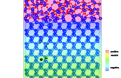
Radiating particles such as gamma ray and neutrons lead to ionizing (generating carriers) and non-ionizing (generating atomic displacements) energy depositions in semiconducting materials, respectively. As a result, the radiation damages of semiconductor devices contain both ionization damage (ID) and displacement damage (DD). In an environment with both gamma ray and neutron radiations, it is often assumed that the total damage is a simple sum of ID and DD. However, recent experiments have demonstrated that, the total damage in bipolar devices could be either smaller or bigger than the simple sum of ID and DD, that is, there is a negative or positive synergistic effect Barnaby et al. (2001, 2002); Gorelick et al. (2004); Li et al. (2010, 2012a, 2012b, 2015a, 2015b); Wang et al. (2015, 2016); Li et al. (2016, 2018). However, the underlying mechanism of the synergistic effects is still not clear. It has been speculated that the gamma-ray-induced charged traps in silica near the silica/silicon interface can change the non-radiative Shockley-Read-Hall (SRH) carrier recombination by modifying charge distributions around the neutron-radiation-induced defects in the base region Barnaby et al. (2001, 2002). For example, in PNP bipolar transistors, the accumulation of the positive oxide trapped charge () near the interface increases the electron density near the base surface by Coulomb attraction (see Fig. 1a). As a result, the SRH recombination current is suppressed because of the widened carrier density difference in the base region, i.e., a negative synergistic effect arises. In NPN devices, a positive synergistic effect would arise because the positive oxide trapped charge lowers the hole density near the base surface through Coulomb repulsion, which reduces the difference of carrier densities in the base region, thus enhances the SRH recombination current. It has also been speculated that the gamma-ray-induced interface traps on the silica/silicon interface can also modify the charge distribution and change the SRH recombination. However, since the interface traps are negative (positive) in N-type (P-type) base region, they always induce a positive synergistic effect for both PNP and NPN transistors Li et al. (2012a, b, 2015a). Very recently, it is deduced from deep level transient spectroscopy (DLTS) signals that the positive synergistic effect in NPN transistors can be enhanced by the displacement defects generated in the oxide layer by low-energy proton radiations, because the defects can induce more oxide trapped charge during sequential high-energy proton radiations Li et al. (2016, 2018). All these models assume that in these processes, the neutron-radiation-induced defect density in the base region is not affected by the gamma ray radiation. However, no systematic study has been carried out to confirm the assumption and moreover, it is not clear what is the dependence of the synergistic effects as functions of the neutron fluence, gamma ray dose, and dose rate.
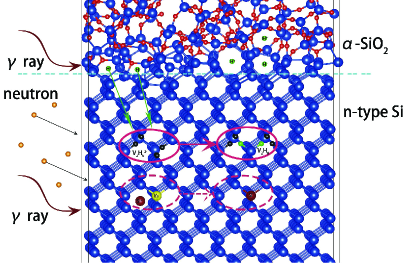
In this work, we carry out systematic investigation on the mechanism of the negative synergistic effects observed in PNP bipolar transistors. The input-stage PNP transistors in the widely used operational amplifiers LM324N are successively radiated by neutron and gamma ray with different neutron fluence, gamma ray dose, and dose rates. We observe a ‘tick’-like dependence on the gamma ray dose on samples radiated by neutrons, from which we identified two negative synergistic effects that have magnitudes comparable with the ID itself. The first one depends linearly on the gamma ray dose, whose slope depends quadratically on the initial DD. The second one has an exponential decay with the gamma ray dose, whose amplitude shows a rather strong enhanced low-dose-rate sensitivity (ELDRS) effect. To explain the observed data, we propose a defect annealing model containing two terms, a carrier-induced defect annihilation in silicon and a proton-induced defect passivation near the silica-silicon interface, which are schematically shown in Fig. 1(b). The simulated results based on the proposed model match the experimental data very well, but differ from previous model that does not consider defect annihilation or passivation. Our unraveled mechanism is important because it implies that, we can repair damaged silicon devices used in space or under other extreme environments by applying appropriate gamma radiation or proton diffusion.
The paper is organized as following. In Sec. II, we describe the experimental setup of the neutron-gamma radiations. In the following Sec. III A, we first show the data, which are found to display clear ‘tick’-like damage-dose profiles. We then demonstrate the presence of two negative synergistic effects in Sec. III B. We then analyze the origin of the two negative synergistic effects in Sec. III C and Sec. III D, respectively. The relative strength of the two negative synergistic effects and experimental conditions for the ‘tick’-like profiles are investigated in the Sec. III E and Sec. III F, respectively. The conclusion is made in Sec. IV.
II Experimental setup
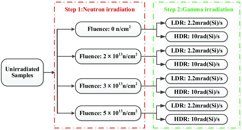
To investigate the behavior of the negative synergistic effect in PNP transistors, LM324N chip (Texas Instruments, TI) with 4 operational amplifiers in each chip was selected for this study. This is because the input stage of the operational amplifier is very straightforward hence the input bias current is directly related to the base current of the input-stage PNP transistors Pease et al. (1996); Barnaby et al. (1999). Based on this fact, the synergistic effect of the input bias current of an LM124 chip, which is very similar to LM324N, has been understood and modeled in the level of the input-stage transistors Barnaby et al. (2001, 2002). On the other hand, with a substrate strucuture and lightly doping, the input-stage transistors in LM324N are sensitive to both neutron and gamma ray radiations, Barnaby et al. (2001, 2002) which is essential for observing a remarkable synergistic effect. The processes of the experiments are shown in Fig. 2. Six neutron-gamma conditions are employed: first neutron radiation with the fluence of 21013/cm2, 31013/cm2, and 51013/cm2, respectively; then gamma radiation to 5krad(Si) at a low dose rate of 2.2 mrad(Si)/s and a high dose rate of 10 rad(Si)/s, respectively. Another two pure gamma radiation conditions are used to obtain the artificial damage. For each condition, we use 2 chips (i.e., 8 PNP transistors). In all the experiments, chips were radiated in an unbiased configuration with all pins shorted. The input bias currents were measured by BC3193 discrete semiconductor testing systems and used to analyze the damages of the input-stage PNP transistors. Neutron radiations were performed at the Chinese Fast Burst Reactor-II (CFBR-II) of Institute of Nuclear Physics and Chemistry, China Academy of Engineering Physics, which provides a controlled 1MeV equivalent neutron radiation. Gamma ray radiations were done at College of Chemistry and Molecular Engineering of Peking University.
III Results and discussion
III.1 ‘Tick’-like dependence on the gamma ray dose
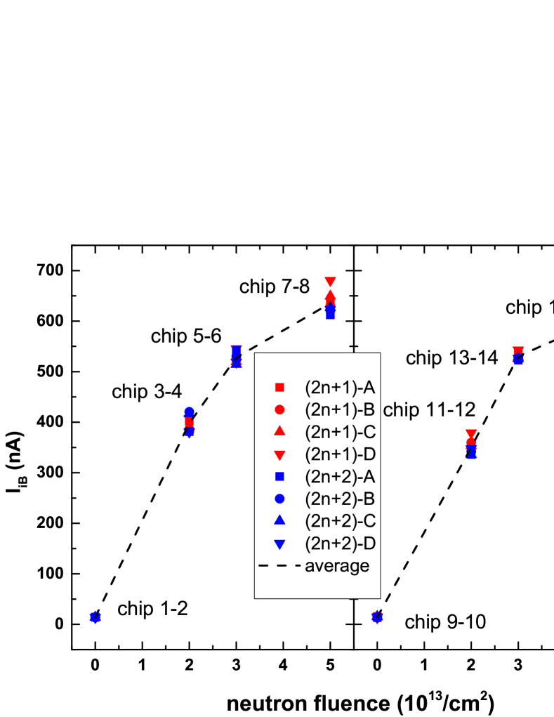
The samples are first radiated by neutrons. Fig. 3 shows the pure DD response of the studied devices. The transistor numbers are indicated in the figure. Also plotted is the average value of the 8 PNP transistors for each neutron fluence. It is seen that, the input bias current () increases sub-linearly with the neutron fluence. When the neutron fluence accumulates from 0 to 51013/cm2, the average bias current increases from about 10 nA to about 600 nA. Due to the different sample quality, the DD of 8 transistors under a same fluence are also different by tens of nA, which will lead to different latter gamma ray response, as discussed below. The thin oxide layer in the PNP transistor is almost transparent for neutrons Raymond and Petersen (1987). Neutron radiation has been shown to introduce acceptor-like defects in Si Li (1995); Lutz (1995); Schulz et al. (1994); Li (1994). The divacancies () and vacancy-oxygen (VO) pairs prominently identified in DLTS measurements Watts et al. (1996); Lindstrom et al. (2001) are thought to be the candidates for these negative charged defect centers Li (1994); Myers et al. (2008); Watts et al. (1996), see Fig. 1(b). Accompanying, Si self-interstitials are also generated. The lifetime of minority carrier () is inversely proportional to the concentration of defects. Pierret and Neudeck (1987) Accordingly, the generation of defects with an increase of neutron fluence results in a persistent decrease of the lifetime of minority carrier and hence the DD degradation, Adell and Boch (2014)
| (1) |
Here the superscript stands for DD, is the charge of minority carrier, is the concentration of intrinsic carriers, and are the area and depth of the space charge region, respectively, is the bias between the base and emitter electrodes, and is the temperature. This relation implies that the concentration of the generated defects is proportinal to the increase of the input bias current, , where . From the data as shown in Fig. 3, we can see that the concentrations of the generated defects in silicon are different for different neutron fluence and samples.
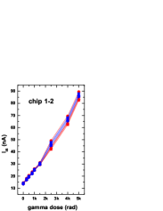
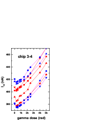
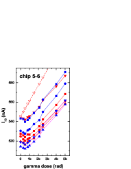
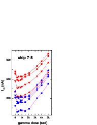
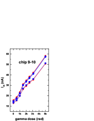
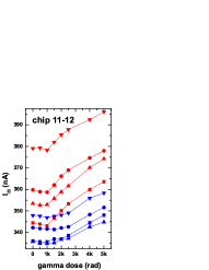
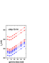
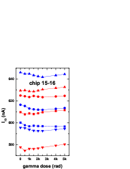
To obtain the simple sum of DD and ID, chips No. 1-2 and No. 9-10 are radiated by gamma ray with low and high dose rate, respectively. The results are displayed in Fig. 4(a) and 4(e), respectively. It is seen that, the ID increases almost linearly with the gamma ray dose, i.e., , where is the gamma ray dose in unit of krad(Si). An average coefficient of nA/krad(Si) and nA/krad(Si) are obtained for the low and high dose rate, respectively. There is a clear ELDRS effect Pease et al. (2008), with an enhancement factor of about 2.3. Under gamma ray radiations, protons are generated in the silica layer through dissociation reactions between oxide trapping charges and hydrogen molecule Rowsey et al. (2011); Yue et al. (2018), see Fig. 1 (b). The generated protons diffuse to the oxide/silicon interface and further generate interface traps () through depassivation reactions on passivated defects Si-H bonds on the interface Rashkeev et al. (2001); Rowsey et al. (2011). The interface traps result in an increase in the surface recombination velocity () above the base region, which leads to the base current increment Schmidt et al. (1996); Kosier et al. (1995)
| (2) |
Here the superscript stands for ID, , where is carrier thermal velocity and is the carrier capture cross section. is the emitter perimeter. From the data in Fig. 4 (a) and (e), it is seen that increases linearly with the gamma ray dose. The concentration of the generated protons is almost constant, which is higher for the low dose rate case.
The simple sum of the DD and ID damages then reads:
| (3) |
where is the initial DD. The result is plotted in Fig. 4(c) for transistor No. 5D. The low-dose-rate gamma response of chips No. 3-8 (24 transistors) with various are shown in Fig. 4 (b-d). Similarly, the high-dose-rate gamma response of chip No. 11-16 (another 24 transistors) are shown in Fig. 4 (f-h). It is seen that, for all 48 samples the total damages are smaller than the simply summed ones. In other words, a clear negative synergistic effect is observed. In previous works Barnaby et al. (2001, 2002), this effect is attributed to the change of the electron density in silicon caused by positive oxide charge accumulation in silica, see Fig. 1(a). However, in this work, our analysis of the features in the data suggest that these effects are due to the annihilation and passivation of the DD defects in silicon.
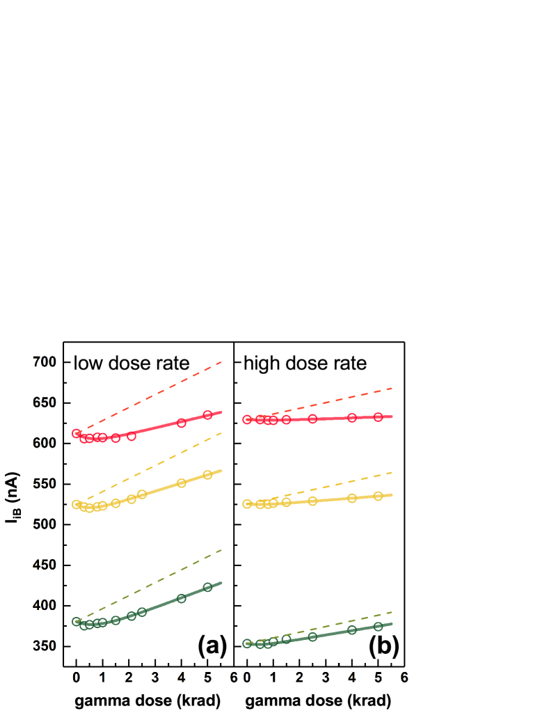
The damages display a ‘tick’-like profile: they abnormally decreases for small gamma ray dose and then increase almost linearly for large gamma ray dose. However, the slope for the latter is obviously smaller than or . In the following, we will show that, they result from the proton passivation and carrier-induced annihilation of the neutron-radiation-induced defects in silicon, respectively.
III.2 Linear and exponential negative synergistic effects and their fluence and dose rate dependence
To obtain a general trend as a function of the initial displacement damage and gamma ray dose rate, in Fig. 5, we plot six typical damage-dose curves: three with of about 380nA, 520nA, and 610nA radiated with the low dose rate, and three with of about 350nA, 520nA, and 630nA radiated with the high dose rate. It is seen that, the larger the initial DD, the bigger the decrease in the slope at large gamma ray dose; on the other hand, the lower the dose rate, the stronger the abnormal decrease of the damage at small gamma ray dose.
To further investigate the possible origin of these two synergistic effects, we fit all the data for the low/high dose rate case in Fig. 4(b-d)/(f-h). Considering both the linear behavior at the large gamma ray dose and the exponential-like decline at the small gamma ray dose in the damage-dose curves, we find that the negative synergistic effects of all 48 curves with different nonzero in Fig. 4 can fit very well to the relatively simple function containing a negative linear term and a negative exponential term,
| (4) |
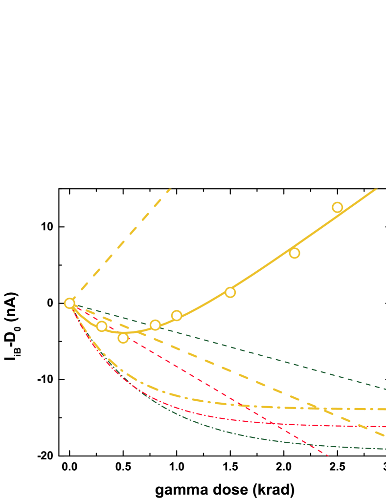
Here is the deviation slope of the linear term; it has a dimension of nA/krad. has a dimension of nA and stands for the amplitude of the exponential decay term. describes the decay rate; its dimension is 1/krad. The fitted curves for the six typical samples are shown in Fig. 5. The individual linear synergistic term and the exponential synergistic term for the 3 curves with different in Fig. 5(a) are shown in Fig. 6 for further analysis. It is clear that, there are two separate negative synergistic effects in the investigated system.
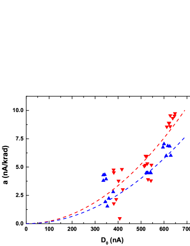
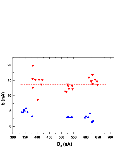
The fitting decay rate () is found to be insensitive to the neutron fluence or gamma ray dose rate. It is almost the same (/krad) for all 48 damage-dose curves. The fitting parameters and as a function of for samples radiated at the low/high dose rate are shown in Fig. 7 (a) and (b), respectively. It is seen that, the decrease in the slope of the damage () increases with superlinearly. Further fitting of the - data shows that, an interesting and simple relation is satisfied for both the low and high dose rates,
| (5) |
where =21/(mA krad) and =16/(mA krad) for the low and high dose rate case, respectively. On the other hand, the amplitude of the exponential term () shows a strong dose rate dependence and is not very sensitive to the initial displacement damage.
III.3 Dependence of the linear synergistic effect on the neutron fluence: carrier-induced defect annihilation in silicon
We first consider the origin of the linear synergistic effect. According to Eqs. (4) and (5), the linear synergistic term can be re-written as
| (6) |
This expression suggest the following. 1) The term depends exactly on , which means that this synergistic effect is related to the neutron-induced defects in silicon; 2) The term is negative, which means that the neutron-induced defects is reduced. In other words, an annealing effect of the neutron-induced defects in silicon happens. 3) The term is a quadratic function of the defect concentration, which suggest that the annihilation of two kinds of related defects happens; 4) The term also depends linearly on the gamma ray dose, which means that the annihilation of the neutron-induced defects is induced by gamma-induced charge carriers.
This observation clearly cannot be attributed to the charge redistribution in the silicon region as implied in early models. Barnaby et al. (2001, 2002); Li et al. (2012a, b, 2015a) Here, we propose that the defect annihilation can be described by the following annihilation reaction
| (7) |
where is the vacancy and is the Si interstitial, both of which are charged by the gamma radiation, see Fig. 1(b). We note that the annihilation of defects in silicon due to injected charge carriers has been found in the past Gregory and Sander (1967); Barnes (1969); Harrity and Mallon (1970) and the origin has been attributed to the enhanced mobility of defects through alternating capture and lose of electrons. Kimerling et al. (1975); Kimerling (1976); Bar-Yam and Joannopoulos (1984a, b); Car et al. (1984) Among various defects, the isolated Si interstitial defects are mobile particles. From this reaction, we can see that, for a fixed gamma ray dose rate, the more the neutron-induced defects exist in the sample the easier to find as well as . On the other hand, for a fixed defect concentration, the more the charge carriers ([h]) are excited by the -ray, the more the mobile defects are stimulated. According to the chemical reaction rate equation, the annihilation rate of the vacancies reads , where is the reaction rate constant between the excited vacancies and interstitials. A simple calculation gives , where is the gamma ray dose. Here the defect concentrations on the right side in the reaction rate equation are much larger than the change and are regarded as constants during the gamma ray radiation. Recalling the relation between the defect concentration and DD, , the above relation can be rewriten as . This is just Eq. (6), with corresponding to . As mentioned above, the value is a slightly larger for the low dose rate case (21/(mA krad)) than for the high dose rate (16/(mA krad)), with an enhancement factor of about 1.3. This means that there is also an ELDRS effect in the linear synergistic effect. It can be conclued that, the square law come from the fact that, the annihilation requires the existence of both interstitial and vacancy; while the interstitial defect caused by the neutral radiation has the same quantity as the vacancy defect.
III.4 Dependence of the exponential synergistic effect on the gamma ray dose rate: proton-induced defect passivation near the silica-silicon interface
Having understood the origin of the linear synergistic effect, we now investigate what is the origin of the exponential synergistic effect, in Eq. (4). As we can see in Fig. 7 (b), the amplitude of the exponential synergistic term () shows an evident ELDRS effect. For the lower dose rate, has a higher value of about 13.5nA, while for the higher dose rate, has a smaller value of about 3.0nA. Accordingly, the enhancement factor is 4.5, which is about two times of that for the pure ID, see Figs. 4 (a) and (e). As mentioned before, protons play a central role in the ELDRS effect of the ID. Pease et al. (2008) Thus, the strong ELDRS effect of the exponential synergistic effect suggests proton is involved in the process. To test this assumption, we did further analysis in the following.
Some experiments and theories have shown that, hydrogen can penetrate the a-SiO2/Si interface Pantelides et al. (2000) and diffuse into Si Sopori et al. (1996); Hanoka (1986); Van de Walle et al. (1988). Further, other experiments and theories also show that, hydrogen is capable of passivating various types of acceptor-like defects and extended defects in Si Sopori et al. (1996); Corbett et al. (1991); Hanoka (1986); Witczak et al. (1998); Pearton (1985); Zhang and Branz (2001); Johnson (1985); Assali and Leite (1985); Mathiot (1989); Pearton et al. (1992); Sana et al. (1994); Bourret-Sicotte et al. (2017). Many types of complex have been proposed, including , , , , etc Corbett et al. (1991); Zhang and Branz (2001); Gerasimenko et al. (1978). The representative reactions can be described as
| (8) |
where is electrically non-active, see Fig. 1(b). These reactions remove the band-gap levels in silicon thus reduce the recombination rate (decrease the displacement damage).
Supposing the concentration of contributes a base current of . From Figs. 5 and 7(b), it is clear that, (about several nA) is much less than (about hundreds of nA). This means that, the concentration of is much fewer than the total amount of the neutron-induced defects in silicon. Thus, not many protons are required to totally anneal the former defects. The relation also means that, the reaction of Eq. (8) can cause sensible changes to the concentration of . In other words, the concentration is an explicit function of time, . From Eq. (8), the decay rate of is , where measures the reaction rate between the defects and protons. Integrating the equation, the defect concentration as a function of time (gamma ray dose) is obtained as
| (9) |
where we have replaced with . Accordingly, the input bias current changes from to , which results in a current decrease of
| (10) |
Eq. (10) has the same form as the exponential term in Eq. (4), with the amplitude corresponding to the fitting factor and the effective decay rate corresponding to the fitting factor .
The reasons for the strong ELDRS effect of the amplitude of the exponential synergistic effect can be explained as following. 1) For the lower dose rate, more protons are generated in silica as a result of the ELDRS effect of the ID, so more protons can diffuse into silicon and leads to a larger passivation. 2) For the lower dose rate, there is a much longer time for protons to diffuse into silicon, which further increases the difference of the amount of the protons in silicon. So, it can be concluded that, the exponential synergistic effect stems from the defect passivation near the silica-silicon interface, which is induced by protons diffusing from the silica, see Fig. 1(b).
The variable or shows no evident dependence on or the gamma ray dose rate. This is because it measures an intrinsic interaction strength, whose value does not depend on the concentrations of the reactants ( and ), which are determined by or the dose rate.
III.5 The relative strength of the two synergistic effects
By combining Eqs. (2), (6), and (10), the practical neutron-gamma damage is described by the following equation:
| (11) |
It is clear that, the practical damage deviates from the simple summed one () by two synergistic effects, namely the carrier-induced linear annihilation, , and the proton-induced exponential passivation, . This is very different from the existing mechanism: Coulomb interaction induced change in the concentration of charge carriers in silicon. Now an important question would arise: How strong are the two synergistic effects? Should them be weak enough that they can be neglected? To answer this question, we derive the changing rates of the input bias currents by taking derivative of in Eq. (11) with respect to . The result is
| (12) |
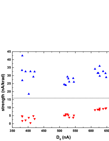
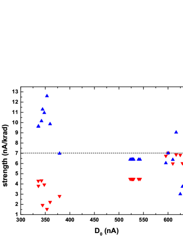
Thus, the strength for each effect can be defined as the corresponding slope, which reads , , and for the ID, the carrier-indued linear annihilation, and the proton-induced exponential passivation, respectively. It is seen that, the strength for the proton-induced passivation decays with the time. In the following, we would like to discuss the initial strength . The values of and are plotted in Fig. 8 (a) and (b) for the low and high dose rate, respectively. The values of and are indicated by the dashed lines. For the low dose rate case, it is seen that, the strength of the carrier-induced annihilation, which increases with the initial DD, is a little smaller than the strength of the ID, while the initial strength of proton-induced passivation is stronger than the stength of the ID. The cases for the three typcial samples radiated with the low dose rate can be clearly seen in Fig. 6. For the high dose rate case, both the carrier-induced annihilation and the proton-induced passivation are comparable with the ID. So, although the two negative synergistic effects (of the order of nA) are much smaller than the initial DD (of the order of hundreds of nA), they are comparable with the ID.
It is interesting that, the initial strength of the proton-induced passivation () is larger than the strengh of the carrier-induced annihilation (), although the population of the defects involved in the former () is about two order of magnitudes smaller than the population of the defects involved in the latter (). The reason is that, the reactions in the proton-induced passivation are much easier than the reactions in the carrier-induced annihilation, because the defects in the former contain dangling bonds and the binding energy with protons are negative Corbett et al. (1991); Zhang and Branz (2001); Gerasimenko et al. (1978).
III.6 Conditions for the ‘tick’-like profiles and specific damages
The ‘tick’-like damage-dose profiles in Figs. 4 and 5 are essential to obtain the two negative synergistic effects. In this last subsection, we will try to investigate under which neutron fluence such a profile can arise. To further verify the proposed model (Eq. (11)), we will also calculate under what gamma ray dose the damage will become the minimal or the same as the initial one, and compare the results with the experiment data.
From Eq. (12), it is readily seen that, if the sum of the (initial) strengths of the two synergistic effects are larger than the strength of the ID, the positive ID term will be overwhelmed and the damage-dose curves will show the declining behaviors. For large enough gamma ray dose, the strength of the proton-induced passivation almost vanishes and the damage-dose curves show ascending behaviors, provided the strength of the ID is stronger than that of the linear annealing. So, the conditions to display a ‘tick’-like profile is that, the ID is smaller than the sum of two annealing effects but larger than the linear annihilation effect. In the view of initial DD (neutron fluence), this means that the carrier-induced annealing should be stronger than the difference between the ID and the proton-induced passivation, but smaller than the ID itself,
| (13) |
For the low dose rate, we obtain 872.9 nA for the appearance of the ascending behavior at large gamma ray dose and no requirement for the declining behaviors at the small dose. For the high dose rate, we obtain 237.2 nA 661.4 nA for the appearance of the ‘tick’-like profiles. These conditions are consistent with the experimental data in Fig. 4. On the other hand, we have obtained monotonously decreasing damage-dose profiles with high gamma ray dose rate for of about 1000 nA (using neutron fluence of 11014/cm2).
At a gamma ray dose where the derivative of the input bias current on the gamma ray dose becomes zero, the damage reaches its minimal value. From Eq. (12), the gamma ray dose is obtained as
| (14) |
where and . Physically, this equation means that, at the specific dose of the decrease rate of the base current due to the two kinds of defect annealing in silicon equals to the increase rate of the base current due to the defect generation on the interface. Inserting this condition into Eq. (11), the minimal current is obtained as
| (15) |
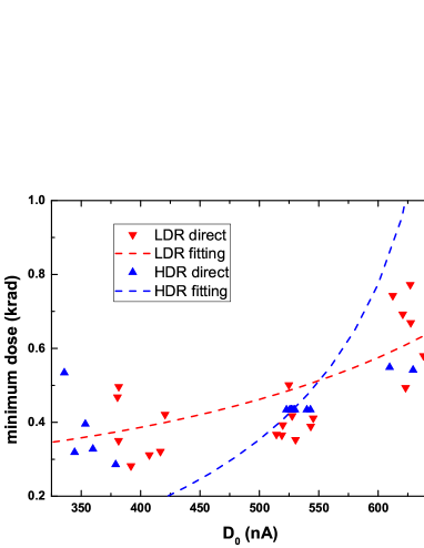
The calculated curve using Eq. (14) is shown in Fig. 9 (a) for both the high and low dose rates. Also shown are the dose values for each sample, which is directly read from the data in Fig. 4. For the low dose rate case, the calculated curve is found to have good agreements with the experimental data, further implying the validity of the proposed model. However, for the high dose rate case, the agreement is only good for the curves with initial DD of about 530nA in Fig. 4 (g). This is because the dose step of 0.5krad (total dose of 5krad) is too large (small) for the curves with of about 350nA (610nA) in Fig. 4f (4h) and the true dose values can be easily missed. From the model predictions, it is also seen that, for both the high and low dose rates, the dose condition for the minimal damage increases for the increasing .
For certain larger gamma ray dose, the damage returns to the initial value before gamma radiation (i.e., ), which we can call as a critical dose. Solving Eq. (11) with the condition of , the critical gamma ray dose is obtained as
| (16) |
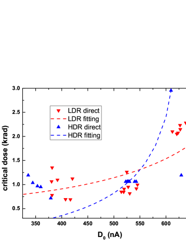
where is Lambert-W function or product logarithm. Physically, this equation means that, at the specific dose of the base current due to the two kinds of defect annealing in silicon equals to the base current due to the defect generation on the interface. Again the calculated curve using Eq. (16) and the experimental data are shown in Fig. 9 (b), which are found to be in good agreement with each other for the low dose rate case. For the high dose rate case, the agreement is bad for the samples with of about 350nA (610nA), due to the too large dose step (too small total dose). It can be seen that, for both the high and low dose rates, the critical dose depends monotonously on the initial DD.
It has been noticed that, the ratio of the strength of the proton-induced passivation () and the sum of the strengths of the ID and the charge-induced annihilation () plays a crucial role in all the critical parameters in Eqs. (14)-(16). This result reveals the significance of the cooperation of the ID and the two synergistic effects.
IV Conclusion
In summary, we have systematically studied the behavior and mechanism of the synergistic effects of neutron and gamma ray radiation by performing successive neutron-gamma radiation experiments on input-stage PNP transistors in operational amplifier LM324N. We find that the measured input bias current obey a ‘tick’-like damage-dose curve. Two negative synergistic effects, both of which are comparable with the ID itself, have been derived from the experimental observation. The first one is caused by a carrier-induced defect annihilation in silicon; it displays as a linear function of the gamma ray dose whose slope depends quadratically on the initial DD of the samples. The second one is caused by a proton-induced defect passivation near the silica/silicon interface; it displays as an exponential function of the gamma ray dose whose amplitude shows a very strong ELDRS effect. The validity of the proposed model is also verified by the prediction of the dose for the minimal and critical synergistic damage. Our proposed mechanism demonstrates that, the ID can influence DD by decreasing the concentration of defects in it, therefore, this technique can be applied to repair devices used in the space and other extreme environments.
The authors thank Professor Chun Zheng of Institute of Nuclear Physics and Chemistry, CAEP for his kindly help in neutron radiation experiments. This work was supported by the Science Challenge Project under Grant No. TZ2016003-1 and NSFC under Grant Nos. 51672023; 11634003; U1530401.
References
- Barnaby et al. (2001) H. J. Barnaby, R. D. Schrimpf, A. L. Sternberg, V. Berthe, C. R. Cirba, and R. L. Pease, IEEE Transactions on Nuclear Science 48, 2074 (2001).
- Barnaby et al. (2002) H. J. Barnaby, S. K. Smith, R. D. Schrimpf, D. M. Fleetwood, and R. L. Pease, IEEE Transactions on Nuclear Science 49, 2643 (2002).
- Gorelick et al. (2004) J. L. Gorelick, R. Ladbury, and L. Kanchawa, IEEE transactions on nuclear science 51, 3679 (2004).
- Li et al. (2010) X. Li, H. Geng, C. Liu, Z. Zhao, D. Yang, and S. He, IEEE Transactions on Nuclear Science 57, 831 (2010).
- Li et al. (2012a) X. Li, C. Liu, H. Geng, E. Rui, D. Yang, and S. He, IEEE Transactions on Nuclear Science 59, 439 (2012a).
- Li et al. (2012b) X. Li, C. Liu, E. Rui, H. Geng, and J. Yang, IEEE Transactions on Nuclear Science 59, 625 (2012b).
- Li et al. (2015a) X. Li, C. Liu, and J. Yang, IEEE Transactions on Nuclear Science 62, 1375 (2015a).
- Li et al. (2015b) X. Li, C. Liu, J. Yang, and G. Ma, IEEE Transactions on Nuclear Science 62, 555 (2015b).
- Wang et al. (2015) C. Wang, X. Bai, W. Chen, S. Yang, Y. Liu, X. Jin, and L. Ding, Nuclear Instruments and Methods in Physics Research A 796, 108 (2015).
- Wang et al. (2016) C. Wang, W. Chen, Z. Yao, X. Jin, Y. Liu, S. Yang, and Z. Wang, Nuclear Instruments and Methods in Physics Research A 831, 322 (2016).
- Li et al. (2016) X. Li, P. Li, J. Yang, and C. Liu, in Radiation and Its Effects on Components and Systems (RADECS), 2016 16th European Conference on (IEEE, 2016) pp. 1–4.
- Li et al. (2018) X. Li, J. Yang, C. Liu, G. Bai, W. Luo, and P. Li, Microelectronics Reliability 82, 130 (2018).
- Pease et al. (1996) R. Pease, W. Combs, A. Johnston, T. Carriere, C. Poivey, A. Gach, and S. McClure, in 1996 IEEE Radiation Effects Data Workshop. Workshop Record. Held in conjunction with The IEEE Nuclear and Space Radiation Effects Conference (IEEE, 1996) pp. 28–37.
- Barnaby et al. (1999) H. Barnaby, R. Schrimpf, R. Pease, P. Cole, T. Turflinger, J. Krieg, J. Titus, D. Emily, M. Gehlhausen, and S. Witczak, IEEE transactions on Nuclear Science 46, 1666 (1999).
- Raymond and Petersen (1987) J. Raymond and E. Petersen, IEEE Transactions on Nuclear Science 34, 1621 (1987).
- Li (1995) Z. Li, IEEE Transactions on Nuclear Science 42, 224 (1995).
- Lutz (1995) G. Lutz, Nuclear Instruments and Methods in Physics Research Section B: Beam Interactions with Materials and Atoms 95, 41 (1995).
- Schulz et al. (1994) T. Schulz, H. Feick, E. Fretwurst, G. Lindstrom, M. Moll, and K. H. Mahlmann, IEEE Transactions on Nuclear Science 41, 791 (1994).
- Li (1994) Z. Li, Nuclear Instruments and Methods in Physics Research Section A: Accelerators, Spectrometers, Detectors and Associated Equipment 342, 105 (1994).
- Watts et al. (1996) S. J. Watts, J. Matheson, I. H. Hopkins-Bond, A. Holmes-Siedle, A. Mohammadzadeh, and R. Pace, IEEE Transactions on Nuclear Science 43, 2587 (1996).
- Lindstrom et al. (2001) G. Lindstrom, M. Ahmed, and S. e. a. Albergo, Nuclear Instruments and Methods in Physics Research Section A: Accelerators, Spectrometers, Detectors and Associated Equipment 466, 308 (2001).
- Myers et al. (2008) S. M. Myers, P. J. Cooper, and W. R. Wampler, Journal of Applied Physics 104, 044507 (2008).
- Pierret and Neudeck (1987) R. F. Pierret and G. W. Neudeck, Advanced semiconductor fundamentals, Vol. 6 (Addison-Wesley Reading, MA, 1987).
- Adell and Boch (2014) P. Adell and J. Boch, Proc NSREC Short Course (2014).
- Pease et al. (2008) R. L. Pease, R. D. Schrimpf, and D. M. Fleetwood, in Radiation and Its Effects on Components and Systems (RADECS), 2008 European Conference on (IEEE, 2008) pp. 18–32.
- Rowsey et al. (2011) N. L. Rowsey, M. E. Law, R. D. Schrimpf, D. M. Fleetwood, B. R. Tuttle, and S. T. Pantelides, IEEE Transactions on Nuclear Science 58, 2937 (2011).
- Yue et al. (2018) Y. Yue, P. Li, Y. Song, and X. Zuo, Journal of Non-Crystalline Solids 486, 1 (2018).
- Rashkeev et al. (2001) S. Rashkeev, D. Fleetwood, R. Schrimpf, and S. Pantelides, Physical review letters 87, 165506 (2001).
- Schmidt et al. (1996) D. Schmidt, A. Wu, R. Schrimpf, D. Fleetwood, and R. Pease, IEEE Transactions on Nuclear Science 43, 3032 (1996).
- Kosier et al. (1995) S. Kosier, A. Wei, R. Schrimpf, D. Fleetwood, M. DeLaus, R. Pease, and W. Combs, IEEE transactions on Electron Devices 42, 436 (1995).
- Gregory and Sander (1967) B. Gregory and H. Sander, IEEE Transactions on Nuclear Science 14, 116 (1967).
- Barnes (1969) C. Barnes, IEEE Transactions on Nuclear Science 16, 28 (1969).
- Harrity and Mallon (1970) J. Harrity and C. Mallon, IEEE Transactions on Nuclear Science 17, 100 (1970).
- Kimerling et al. (1975) L. Kimerling, H. DeAngelis, and J. Diebold, Solid State Communications 16, 171 (1975).
- Kimerling (1976) L. Kimerling, IEEE Transactions on Nuclear Science 23, 1497 (1976).
- Bar-Yam and Joannopoulos (1984a) Y. Bar-Yam and J. Joannopoulos, Physical Review B 30, 1844 (1984a).
- Bar-Yam and Joannopoulos (1984b) Y. Bar-Yam and J. Joannopoulos, Physical Review B 30, 2216 (1984b).
- Car et al. (1984) R. Car, P. J. Kelly, A. Oshiyama, and S. T. Pantelides, Physical Review Letters 52, 1814 (1984).
- Pantelides et al. (2000) S. T. Pantelides, S. N. Rashkeev, R. Buczko, D. M. Fleetwood, and R. D. Schrimpf, IEEE Transactions on Nuclear Science 47, 2262 (2000).
- Sopori et al. (1996) B. L. Sopori, X. Deng, J. P. Benner, A. Rohatgi, P. Sana, S. K. Estreicher, Y. K. Park, and M. A. Roberson, Solar Energy Materials and Solar Cells 41-42, 159 (1996).
- Hanoka (1986) J. I. Hanoka, in Hydrogen in Disordered and Amorphous Solids, NATO ASI Series, Vol. 136, edited by G. Bambakidis and R. C. Bowman (Springer US, Boston, MA, 1986) pp. 81–90.
- Van de Walle et al. (1988) C. G. Van de Walle, Y. Bar-Yam, and S. T. Pantelides, Phys. Rev. Lett. 60, 2761 (1988).
- Corbett et al. (1991) J. W. Corbett, P. Deák, U. V. Desnica, S. J. Pearton, J. I. Pankove, and N. M. Johnson, in Semiconductors and Semimetals, Vol. 34 (Elsevier, 1991) pp. 49–64.
- Witczak et al. (1998) S. C. Witczak, R. C. Lacoe, D. C. Mayer, D. M. Fleetwood, R. D. Schrimpf, and K. F. Galloway, IEEE Transactions on Nuclear Science 45, 2339 (1998).
- Pearton (1985) S. J. Pearton, in Thirteenth International Conf. on Defects in Semiconductors, Metallurgical society of AIME, edited by L. C. Kimerling and J. M. Parsey (Warrendale, PA,, 1985) p. 737.
- Zhang and Branz (2001) S. B. Zhang and H. M. Branz, Phys. Rev. Lett. 87, 105503 (2001).
- Johnson (1985) N. M. Johnson, Phys. Rev. B 31, 5525 (1985).
- Assali and Leite (1985) L. V. C. Assali and J. R. Leite, Phys. Rev. Lett. 55, 980 (1985).
- Mathiot (1989) D. Mathiot, Phys. Rev. B 40, 5867 (1989).
- Pearton et al. (1992) S. J. Pearton, J. W. Corbett, and M. Stavola, Hydrogen in Crystalline Semiconductors, Springer Series in Materials Science, Vol. 16 (Springer-Verlag, Berlin, 1992).
- Sana et al. (1994) P. Sana, A. Rohatgi, J. P. Kalejs, and R. O. Bell, Appl. Phys. Lett. 64, 97 (1994).
- Bourret-Sicotte et al. (2017) G. Bourret-Sicotte, P. Hamer, R. S. Bonilla, K. Collett, and P. R. Wilshaw, Energy Procedia 124, 267 (2017).
- Gerasimenko et al. (1978) N. N. Gerasimenko, M. Rolle, L.-J. Cheng, Y. H. Lee, J. C. Corelli, and J. Corbett, physica status solidi (b) 90, 689 (1978).