Time resolution and dynamic range of field effect transistor based terahertz detectors
Abstract
We studied time resolution and response power dependence of three terahertz detectors based on significantly different types of field effect transistors. We analyzed the photoresponse of custom-made Si junctionless FETs, Si MOSFETs and GaAs-based high electron mobility transistors detectors. Applying monochromatic radiation of high power, pulsed, line-tunable molecular THz laser, which operated at frequencies in the range from 0.6-3.3 THz, we demonstrated that all these detectors have at least nanosecond response time. We showed that detectors yield a linear response in a wide range of radiation power. At high powers the response saturates varying with radiation power as , where is the low power responsivity, is the saturation power. We demonstrated that the linear part response decreases with radiation frequency increase as , whereas the power at which signal saturates increases as . We discussed the observed dependences in the framework of the Dyakonov-Shur mechanism and detector-antenna impedance matching. Our study showed that FET transistors can be used as ultrafast room temperature detectors of THz radiation and that their dynamic range extends over many orders of magnitude of power of incoming THz radiation. Therefore, when embedded with current driven read out electronics they are very well adopted for operation with high power pulsed sources.
I Introduction
Photovoltaics based on plasma oscillations is considered as the main candidate for robust and highly sensitive room temperature THz photodetectors, see e.g. x3 ; Vicarelli ; x1 ; x2 ; x4 ; x5 . Plasmons are high-frequency oscillations of the electron gas density and occur in many metals and semiconductors. A boost to the plasma wave semiconductor electronics was given at early 90s, when M. Dyakonov and M. Shur predicted a -current-induced plasma wave instability in nanometer sized channels of field-effect transistors (FET) and demonstrated that FET can be used for efficient detection of microwave/terahertz radiation Dyakonov ; Dyakonov2 . The instability results in the generation of plasma oscillations. Due to the high velocity of these plasma waves ( cm/s) the frequency of the oscillations can be easily tuned (e.g., applying a gate voltage) into the THz frequency range Dyakonov ; Dyakonov2 . Furthermore, in high mobility structures plasmonic resonances result in a drastic increase of the dc signal response to THz radiation. Robust room temperature FET plasmonic detectors being characterized by large detectivity (D∗) and, correspondingly, low noise equivalent power (NEP) has become an important technology for THz applications. Main nowadays demonstrated THz technology applications are nondestructive quality control or security screening. In case of highly absorbing media (opaque or very thick materials/packages) imaging with CW sources suffers from the quickly degrading signal to noise ratio. Indeed, while using continuous wave THz sources even use of the most sensitive detectors does not allow to get sufficiently high image quality. This is because existing CW sources operate in relatively low output power: milli- or microwatt range. This can be re-mediated by use of of high-power terahertz sources such as molecular lasers, free-electron lasers, -Ge lasers difference-frequency-based terahertz systems, impurity laser in stressed bulk and low dimensional semiconductors, etc., see e.g. book ; Lee ; Zhang ; Bruendermann ; Elsaesser , besides D∗ and NEP. These sources can reach powers up to a few watts however they always operate in the pulsed mode. Therefore, while studying FETs for imaging applications with these sources one has to consider not only FET responsivities but also additional figures of merit like time resolution, and dynamic range. The later has been rarely addressed in the previous studies but is really important in the imaging. This is because during scanning of highly attenuating media/objects, with high power sources, the power of THz beam reaching detector increases by many orders of magnitude while reaching the boarder of the object. This often leads even to breakdown of many of the standard detectors like for example Schottky diodes. On the other hand many of the robust standard detectors like for example Si-bolometers are not fast enough to be used with high-power pulsed sources. Former characteristic is also important for wireless communication, for which FET are considered as a promising candidate because this solution guarantees low fabrication costs and easy on-chip integration with potential readout electronic. The purpose of this work is to study FET as detectors for high power short pulsed THz sources.
Here we present a systematic study of these characteristics of three different types of the state-of-the-art plasma based detectors. We analyse photoresponse of a custom-made detector Si junctionless FET (JLFET), Si metal oxide semiconductor FET (Si-MOS) and InGaAs/GaAs-based high electron mobility transistors (HEMT) transistors, which represent structures that are very often employed in experiments dedicated to detection of sub-THz and THz radiation using FETs. All structures have been monolithically integrated with a log-periodic broad-band planar antenna. Time resolved photoresponse of room temperature detectors have been studied applying nanosecond pulses of monochromatic linearly polarized terahertz laser radiation with frequencies ranging from 0.6 to 3.3 THz. Our measurements explore time resolution, detectors nonlinearity, and polarization dependence for different gate voltages applied to FET transistors operating with two types of amplifiers. We show that indeed FET detectors, while embedded with specific read-out circuits (current driven) are well adapted (low NEP, high dynamic range) for high power pulsed laser based applications.
I.1 Devices and characteristics
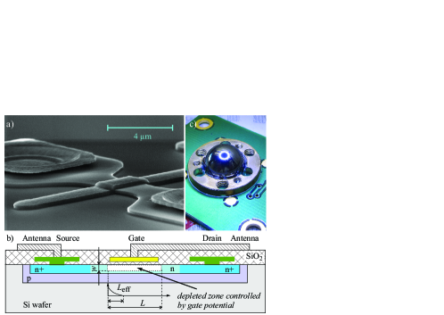
Figure 1 shows scanning electron microscopy image and sketch of the first structure: Junctionless FET fabricated in Institute of Electron Technology, Poland. JLFET is a device with a layout that is similar to classical MOSFET one, however, in contrast to classical MOSFETs, the source, drain and channel areas of JLFET are made of the same type of semiconductor (- and -type), see Fig. 1(b). The JLFET detector has been fabricated on high resistivity silicon wafer. Regions of -type well and -type channel were subsequently diffused. Further processing steps included gate thermal oxidation (thickness 25 nm), poly-Si gate preparation (thickness 400 nm), and Al:Si metal contact fabrication. The log-periodic antenna described below was also made of this metal layer. The source-drain current in JLFET can be varied by the thickness of the conducting channel below the depleted zone controlled by the gate voltage . The -- conduction path has -area of carrier density cm-3, which has been choosen to control the conduction channel by gate voltages within a reasonable range. Note that our junctionless FET remains conductive even without the gate voltage and closes at -0.4 V threshold voltage . To minimize any parasitic gate-source and gate-drain capacitances the polysilicon gate was deposited at about m distance from source and drain regions, see Fig. 1(b). The detector gate length and width were 5 and m, respectively. The carrier mobility determined from accumulation characteristics was = 154 cm2/(Vs) near the transistor’s threshold voltage V. The effective length , where rectification takes place, was estimated according to Ref. Kachorovskii2013 . For gate voltage and frequency THz we obtained nm. More details on the structure preparation as well as electrical characteristics of the similar structures can be found in Ref. Marczewski2015 ; ProcSPIE2016 .
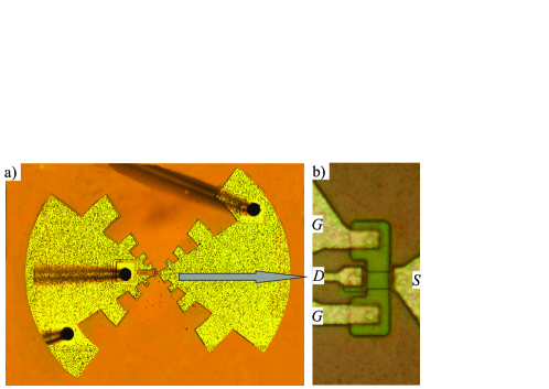
Second structure studied here was silicon MOS transistor, also made in Institute of Electron Technology, Poland. The structure had a classical -type MOSFET design and was fabricated applying CMOS technology (m design rules, poly-Si gate) modified to use a high-resistive substrate, which in this way became part of a glued hyper-spherical silicon lens described below. The gate length and width were 3 and 6 m, respectively. The carrier mobility was = 530 cm2/(Vs) near the threshold V ( nm).
The third structure was HEMT transistor based on epitaxially grown InGaAs/GaAs structure, which have been designed and fabricated within the PH10 GaAs pHEMT process offered commercially by United Monolithic Semiconductors S.A.S (UMS). The channel conductivity could be controlled by the gate voltage from -1.0 to 0.7 V. The gate length was m, the gate width was from 20 m. More details on the HEMT characteristics can be found in Ref. Teyssandier .
Each of these transistors has been monolithically integrated with a broadband log-periodic planar antenna located on the top-most metallization layer, see Fig. 2. The antenna directly feeds the source and the gate contacts of the transistor. The metallization layer is also used to provide the DC-bias voltages to the structure. The voltage is accessible at contact pads located near the outer edge of the lower arm of the antenna. The source electrode was grounded and the output signal, , was detected from a drain electrode. The channel resistance (and detectors responsivity) was controlled by applying a gate voltage . The complete device has been designed as a broadband detector, which requires HR high-resistivity hyper-spherical lens Filipovic . The detector elements has been mounted on the flat side of the lens of diameter 10 mm, see Fig. 1 (c).
I.2 Sources of radiation and methods
Detectors responsivity and noise equivalent power have been measured applying low-power radiation of amplifier-multiplier chain (AMC-10 unit from VDI, Inc.). This source provided monochromatic incident wave of frequency selectable in the band of 0.14 – 0.5 THz. Signals were detected using a lock-in amplifier (SR-830 from Stanford Research Systems, Inc.) synchronized with a low-frequency chopping signal that was modulating the THz source during measurements. The modulation frequency was equal 187 Hz. The beam profile was nearly Gaussian. Measurements were performed without any additional beam shaping elements. The distance between the source and investigated devices was about 30 cm. An estimation of the responsivity given in V/W was obtained by comparison with calibrated detector of the same size, for the details of the method see Ref. Kopyt . The method, which was used instead of calculation power deposited on a detector aperture, allowed us to decrease large systematic error. As a calibrated device, a commercial quasi-optical Schottky diode detector (QOD 1-14 from VDI, Inc.) was used. To calculate NEP per unit bandwidth the Johnson-Nyquist noise was assumed as dominating and took into account.
| Si MOS | JLFET | HEMT | |
|---|---|---|---|
| Responsivity (V/W) | 6 | 0.5 | 150 |
| NEP (W/) |
Time resolution and detectors nonlinearity have been measured by applying high-power line-tunable pulsed molecular gas THz laser ratchet2011 ; Drexler2012 optically pumped by a tunable CO2 laser PRB2002 ; PRBratchet . Using CH3F, D2O, and NH3 as active media, monochromatic laser radiation with frequencies of 0.6, 0.77, 1.07, 2.02, and 3.3 THz were obtained. The laser operated in single pulse regime (repetition frequency 1 Hz) with a pulse duration of about 100 ns. Due to the spontaneous mode-locking the pulse consisted of short spikes with full width half maximum time duration of about 4 ns, which allowed us to analyse time constant of detectors with a a resolution of a several ns. The radiation power has been measured by a calibrated fast room temperature photon drag detector Ganichev85p20 and -photoconductivity detector Ganichev85p377 , both made of -type Ge crystals. These detectors operating in the frequency range for 0.3 to 30 THz, had subpicosecond time resolution and were used as reference detectors for the time resolved measurements. For both reference detectors we used a bandwidth of 300 MHz and a voltage amplification of 46 dB. The radiation was focused by a parabolic mirror. The laser beam had an almost Gaussian shape with full widths at half maximum between 1 mm (at 3.3 THz) and 3 mm (at 0.6 THz) as measured by a pyroelectric camera PhysicaB1999 . The highest peak power and power density used in our measurements at these frequencies were 1 kW and 0.1 W/cm2, respectively. Note that in the used laser peak power varies from pulse to pulse by about 15 %. All measurements have been carried out at room temperature and the devices have been illuminated at normal incidence. To vary the radiation intensity we used a set of teflon, black polyethylene, polyoxymethylene, polyvinyl chloride, and/or pertinax book calibrated attenuators. The photoresponse was amplified and measured using a digital oscilloscope. Two types of amplifiers with substantially different input resistance have been used. The first one was transimpeadance amplifier (TIA) with very small input impedance (), whereas the second one was voltage follower (VF) or, to be more precise, unity-gain voltage amplifier. Amplifiers characteristics are given in Tab. 2.
| Bandwidth | input resistance | output resistance | amplification | |
|---|---|---|---|---|
| (MHz) | DC () | at 10 MHz () | ||
| VF | 108 | 450 k | 2 | 1 V/V |
| TIA | 470 | 50 | 8000 V/A |
The voltage follower is a circuit providing high resistance of its input and relatively low resistance of the output. This circuit reduces the influence of the capacitance of cables connecting the detector under examination with the lock-in system at the expense of the amplitude of the signal. At the same time VF meets the assumption of the Dyakonov theory, which requires a detector to be loaded with a high resistance (open circuit). The transimpedance amplifier is an amplifier whose input current produces an output voltage in a proportional way. Ideally its input should represent a short circuit. Certainly such a circuit is not commonly used for THz radiation detection with FET detectors but allows to avoid a limitation of transmitted bandwidth associated with the output capacitance of the detector. Therefore, such an idea is often used for design of optical amplifiers for telecommunication technology.
Additional measurements on power dependence have been carried out applying CW CH3OH optically pumped laser Olbrich2013 ; Dantscher2015 operating at frequency of 2.54 THz. The laser beam with power mW was modulated at a frequency of Hz. Note that TIA has dB low frequency cutoff at modulation frequency about about 30 kHz, therefore, at our low its amplification coefficient was substantially reduced.
II Results and discussion
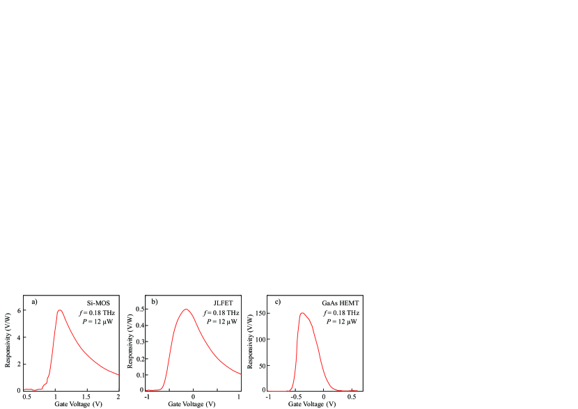
We begin with briefly introducing the results obtained by applying low frequency and low power radiation of radiation of amplifier-multiplier chain zero magnetic field. While the paper is devoted to detector’s time resolution and nonlinearity these results show basic characteristics of our detectors obtained under ”standard” experimental conditions. Results of experiments with linearly polarized low power radiation are shown in Fig. 3. The figure presents a gate voltage dependence of the transistor’s photoresponse measured for radiation frequency of THz and power 12 W. For all transistors the signal shows a maximum for a gate bias close to the threshold voltage, . Such a non-monotonic behavior of the signal is well known for FET detectors Knap2002 ; Sakowicz2011 ; Lusakowski2011 . Responsivities and estimated noise equivalent powers NEP are given in Tab. 1. The values of are smaller and NEP are larger than the best found in literature. In our opinion the reason is that our method of responsivity calculation does not include a size of detector.
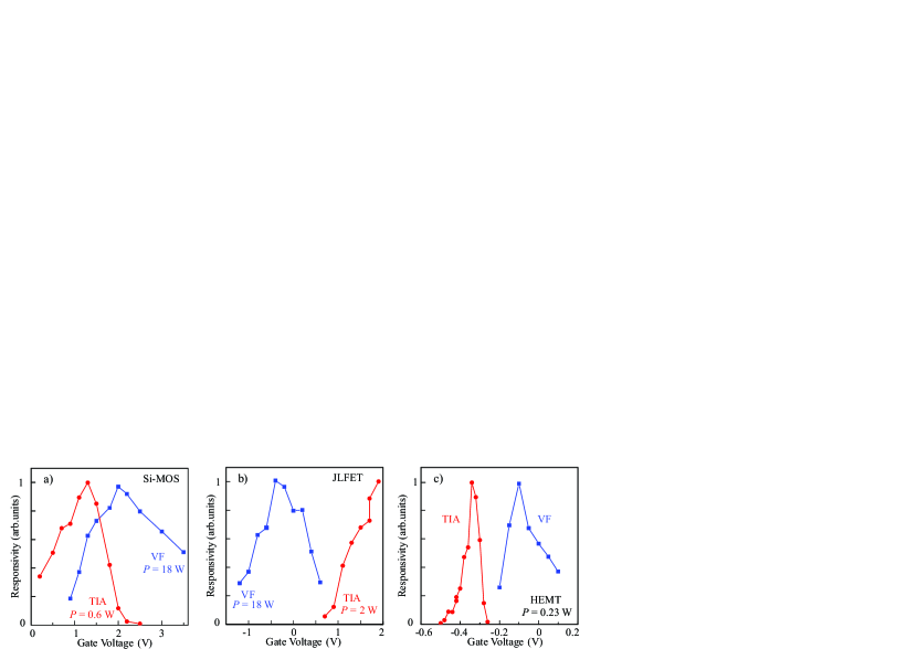
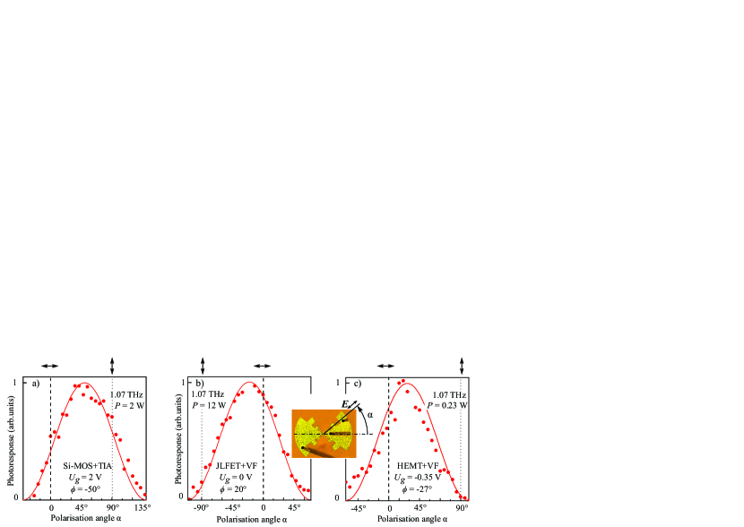
Photoresponse of all three detectors has been obtained by applying pulsed radiation with substantially higher frequencies, including the highest one used in our work, THz. Figure 4 shows gate voltage dependencies obtained for THz. Dependencies were measured with two different amplifiers: the TIA and the VF. While in both cases we obtained nonmonotonic dependencies similar to that measured at THz, see Fig. 3, the maximum position is substantially different for TIA and VF amplifiers. We attribute this fact to more than five order difference in the input resistance, see Tab. 2. These observed differences in location of the maximum responsivity point, as a function of gate voltage, are related to totally different operating point of detecting transistors. The output current of a FET is also affected by its drain to source voltage. In case of the TIA, the output electrode (drain) of the detecting transistor is loaded by a very low input resistance of this read-out amplifier. In contrast to TIA, the VF has input resistance ranging to hundreds of kiloohms. Varying orientation of the radiation electric field vector by means of lambda half plates we observed that the signal follows dependence, where is the photoresponse magnitude and is a phase shift. Such polarization dependence is expected for Dyakonov-Shur FET detectors additionally taking into account the the optimum polarization for radiation-antenna coupling, see e.g. Sakowicz2008 ; Sakowicz2010 ; antenna2005 . Note that in some measurements we also detected a small polarization independent offset. Comparison of the photovoltage distribution with the design of transistors reveal that in JLFET and HEMT detectors the signal achieved a maximum value for the radiation polarization vector aligned nearly parallel to the line connecting the source and drain, being also axis of the antennas, see Fig. 2. In a Si-MOS structure we detected the maximum of the response at an angle about 45∘ to this axis.
Now we turn to the main part of the paper devoted to time resolution, frequency range and nonlinearity of the FET detectors.
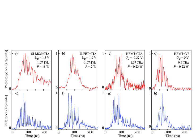
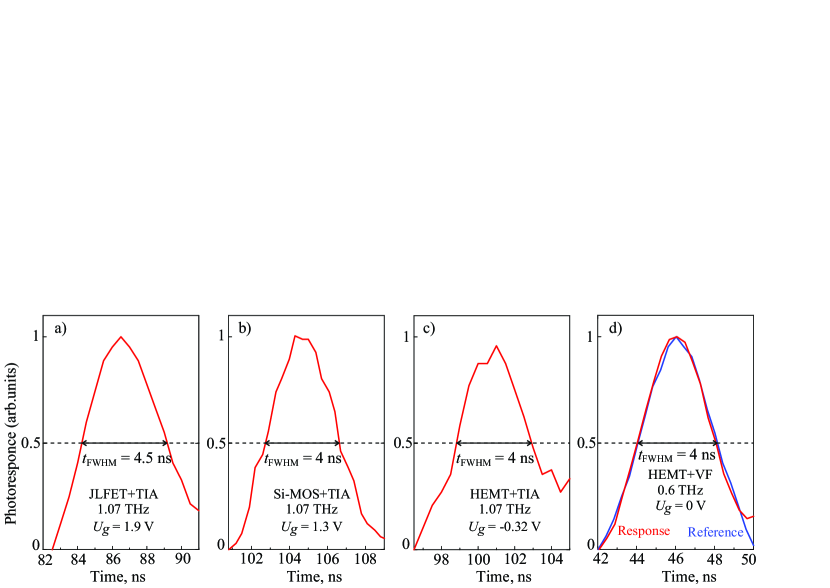
Figures 6(a)-(c) show pulse traces obtained with FET detectors combined with transimpeadance amplifier characterized by its input resistance less than in comparison with the response of the reference photon drag detector. In this case the output terminal (drain) potential was pinned to 0. Under this condition, the response of any detector is usually much faster than if it was loaded with an amplifier with the large input resistance, when RC constant regarding the resistivity of its channel and the output capacitance plays a dominant role. Figure 6(d) proves, however, that the extremely small RC constant typical of modern sub-micron HEMT transistors makes them sufficiently fast, even when they are loaded with the high VF resistance. It is seen that with TIA amplifiers all detectors perfectly reproduce short spikes caused by the spontaneous mode-locking. The same is valid for HEMT at zero gate voltage combined with VF amplifier. Zoom of single spikes are shown in Fig. 7. The full width half maximum (FWHM) time duration, , of all signals registered by FET detectors is about 4 ns. The same time constants are detected by fast reference photon drag detector, see an example in Fig. 7(c), and -photoconductivity detectors (not shown). Consequently, our measurements demonstrate that all three detectors have time resolution better than 4 ns. This result has been obtained for all gate voltages and radiation frequencies. Such a high time resolution of FET detectors is in fully agreement with theoretical results of Ref. Kachorovskii2008 . This paper considered the dynamic response of FET for modulation frequencies lower than radiation frequency. It was shown that theoretical the maximal modulation frequency allowing for adiabatic response is rather high (on the order of 50–100 GHz for a 200 nm gate transistor operating above-threshold and on the order of 5–10 GHz in the below-threshold regime).
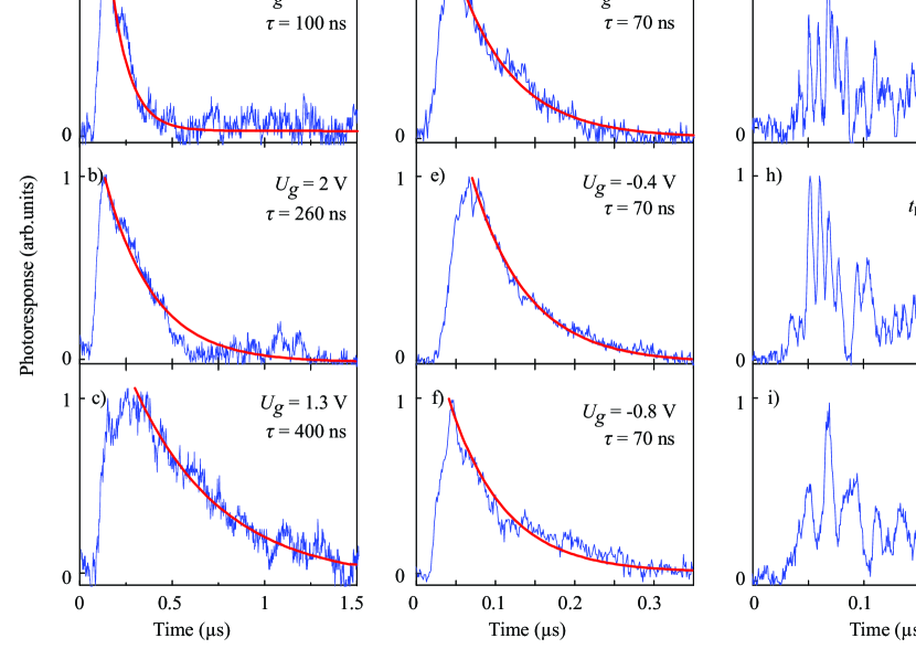
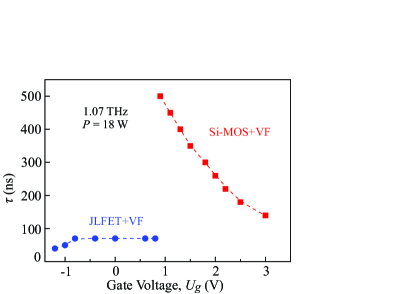
Using the same detector elements with voltage follower we observed a substantial increase of the response time of Si-MOS and JLFET as well as a small increase of the one for HEMT. Furthermore, it becomes dependent on the gate voltage. Typical pulse traces obtained with VF amplifiers are shown in Fig. 8. Figures 8(a)-(f) show that both silicon FETs loaded with VF are much slower comparing to those loaded with TIA, see Figs. 6 and 7. They hardly follow the envelope of the signal and definitely cannot reproduce individual spikes well seen on Fig. 6 as measured by the photon drag detector. In VF configuration the constant of these detectors becomes the most significant factor limiting their speed. Figures 8(a)-(c) show that opening channel of Si-MOSFET (going from 1.3 toward 3.5 V) makes the device faster since the channel opens proportionally to the difference reducing the resistivity of the channel. A more than 20 times increase of the response time is also detected for JLFET, see Figs. 8(d)-(f). In the case of JLFET, the gate bias between -0.8 and 0.6 V has slight influence on the carrier amount in the channel, thus the time constant does not change with the gate voltage. Figure 9 shows the decay time as a function of the gate voltage for both Si-FETs. Figures 8(g)-(i) proves, however, that sub-micron HEMT is a much faster device characterized by extremely small constant (the individual spikes seen by the drag detector are well seen). In this case opening channel (changing from -0.13 V to 0) makes the device only a bit faster.
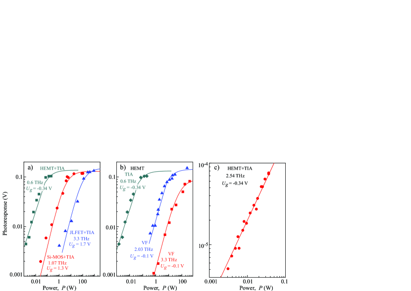
Photoresponse was detected at all frequencies ranging from 0.18 to 3.3 THz and in a wide range of frequencies and radiation power ranging for microwatts to kilowatts. Figure 10(a) shows power dependence of Si-MOS, JLFET and HEMT with TIA amplifiers, i.e. in the regime of the fast response. Power dependences for the fastest of our transistors (HEMT) with both kinds of amplifiers are presented in Fig. 10(b) for pulsed laser radiation and Fig. 10(c) for low power laser radiation. These figures demonstrate that for under all conditions (different radiation frequencies, gate voltages and type of amplifier) the photoresponse behaves in the same way: linear response at low powers changes to its saturation at higher powers. Furthermore, it follows a universal phenomenological equation:
| (1) |
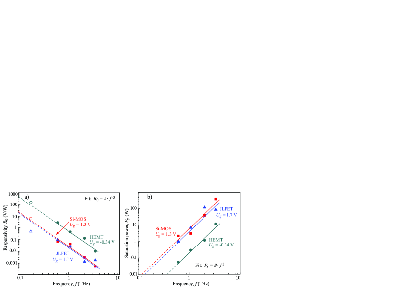
where is the responsivity and is the signal in the linear regime (), and is the saturation power. It is seen that both, the low power linear responsivity and saturation power, depend strongly on the radiation frequency. Frequency dependence of the low power responsivity and saturation power are shown in Figs. 11(a) and (b), respectively. These plots reveal that decreases with radiation frequency as while the saturation power increases with rising frequency as . Studying Si-MOS and JLFET we observed that also in these structures increase of power leads to saturation described by Eq. (1) with and , see Figs 11.
While the observed power dependence given by Eq. (1) is in agreement with the experimental results obtained for InGaAs HEMTs and developed broadband detection model, see But2014 , it contradicts with the results of theoretical analysis of Ref. Gutin . The latter considered nonlinear dependence of the FET response on the power of external radiation for non-resonant detection, when plasma oscillations are overdamped. These regime corresponds to conditions of our experiments. The authors demonstrated that above threshold the photoinduced voltage behaves as:
| (2) |
and below threshold as:
| (3) |
where is the magnitude of the radiation wave (), is the Boltzmann constant, is temperature, is the Bessel function of the imaginary argument, and is the subthreshold ideality factor. In the case of strong signal corresponding to high power these equations predict . Experiment of Ref. Gutin carried out applying low power molecular laser operating at frequency 1.63 THz clearly shows begin of nonlinearity and can be fitted by Eqs. (2) and (3). However, at used low powers, corresponding to a point where the nonlinearities occurr, the data can be well fitted by Eq. (1), too. Analysis of our data obtained in substantially larger range of radiation powers demonstrates that for power levels below saturation power the data can be well fitted for both power dependencies. At powers above the saturation power, however, the photoresponse follows Eq. (1) and can not be described by Eqs. (2) and (3). We note that for high powers a linear decrease of the current responsivity with increase of radiation power has also been calculated in Ref. Lisauskas2018 ; Ikamas20182 . In these works the authors implemented both the standard non-quasi-static FET model and the distributed transistor model and calculated in the Advanced Design System software environment of Keysight Technologies. As compared to Ref. Gutin the authors took into account that in the large signal approximation, the impedance starts to depend on power as well.
Finally we discuss the frequency dependence of the low power responsivity and saturation power. Our data shows that signal of all three transistors having the same antenna design and using Si lens behaves similarly upon variation of radiation frequency yielding . This result can be described in terms of theory of Sachno et al. Sachno2013 considering silicon MOSFET as THz/sub-THz detectors with account of parasitic resistances and capacitances as well as detector-antenna impedance matching Kopyt2015 . The work Ref. Sachno2013 shows that frequency dependence of real detectors depends substantially on above parameters. It has been demonstrated that the responsivity can decrease with the frequency increase as with parameter or 4 depending on the antenna-detector coupling. Fitting curves in Fig. 11(a) show that for our detectors . We emphasize that, as it has recently been demonstrated by Ikamas et al. FET detectors with optimized antenna-transistor coupling requiring also a careful control of beam profile, a nearly flat responsivity could be achieved up to about 1.6 THz, see Ikamas2018 .
As concerning the saturation power it also scales with the third power of radiation frequency increasing with the frequency increase , see Fig. 11(b). It is also the smallest for HEMT, which has the largest responsivity. Currently we have no explanation for this fact, however, we note that in the saturation problems it is quite often that the saturation parameter is coupled to the reciprocal value of the radiation-matter coupling, which, in our case, is included in the low power responsivity. At last but not least we discuss the dynamic range of our detectors. Figure 11(b) reveals that both Si-based FETs have substantially larger (by about 20 times) upper limit of linear detection (defined by saturation power) as compared to HEMT. At the same time NEP of HEMT is times smaller than those of Si-FETs, see Tab. 1. Therefore, the best dynamic range is obtained for HEMT detectors.
III Conclusions
Our study demonstrated that Si-based FET and InGaAs-based HEMT can be used as ultrafast room temperature detectors of terahertz radiation. Applying short pulses of spontaneously mode-locked molecular optically pumped THz lasers we have shown that all examined detectors equipped with low input resistance transimpedance amplifiers had a resolution better than 4 ns. This result reveal that applying current reading method serves ultrafast detection of THz radiation, for HEMT, but, importantly, for Si-FETs as well. Using of high input resistance voltage followers decreases time resolution of Si-based MOS, so that the time constant becomes of the order of hundreds of nanoseconds, whereas HEMT detectors remains fast being characterized by the time constants of the order of several nanoseconds. Investigations of the photoresponse in a wide range of radiation powers and frequencies demonstrated that with the power increase the linear response changes to the signal saturation. This process is well described by empirical equation . The range of linearity and values of saturation powers depends on the radiation frequency. Our data show that the responsivity decreases with the frequency increase as , whereas the saturation power increases as . The latter, depending on the radiation frequency and type of transistor changes from 0.1 up to 600 W. To summarize, we show that field effect transistors equipped with transimpedance amplifiers can be used as ultra-fast room temperature detectors of THz radiation and that the their dynamic range extends over many orders of magnitude of power of incoming THz radiation. Taking into account very low NEP of HEMT we found out that while the saturation power of this detector is the smallest it has by orders of magnitude larger dynamic range. Most of scientists characterize FET-based detectors measuring the THz induced voltage on the open drain terminal. TIA provides measurement of the THz induced current through the short circuited drain. The latter configuration except high dynamic range offers also fast impulse response and excellent signal-to-noise ratio. Therefore, we indeed show that these FETs with current based read-out are well adopted for operating and/or imaging with high power pulsed sources.
Acknowledgements.
We thank V. Kachorovskii and A. Lisauskas for fruitful discussions. Support by the CENTERA, Deutsche Forschungsgemeinschaft (DFG) and the Volkswagen Stiftung Program (90298) is gratefully acknowledged. This study was partially supported by the National Center for Research and Development in Poland grants LIDER/020/319/L-5/13/NCBR/2014, PBS3/B3/30/2015, PBS3/A3/18/2015.References
- (1) W. Knap, M. Dyakonov, D. Coquillat, F. Teppe, N. Dyakonova, J. Lusakowski, K. Karpierz, M. Sakowicz, G. Valusis, D. Seliuta, I. Kasalynas, A. Fatimy, Y. M. Meziani, and T. Otsuji, ”Field effect transistors for terahertz detection: physics and first imaging applications”, J. Infrared Millim. TeraHz Waves 30, 1319 (2009).
- (2) L. Vicarelli, M. S. Vitiello, D. Coquillat, A. Lombardo, A. C. Ferrari, W. Knap, M. Polini, V. Pellegrini, and A. Tredicucci, ”Graphene field-effect transistors as room-temperature terahertz detectors”, Nature Materials 11, 865 (2012).
- (3) W. Knap and M. Dyakonov, in Handbook of Terahertz Technology ed. D. Saeedkia (Woodhead Publishing, Waterloo, Canada 2013), pp. 121-155.
- (4) S. Boppel, A. Lisauskas, and H. G. Roskos, in Handbook of Terahertz Technology ed. D. Saeedkia (Woodhead Publishing, Waterloo, Canada 2013), pp. 231-271.
- (5) S. Preu, H. Lu, M. Sherwin, and A. C. Gossard, ”Detection of nanosecond-scale, high power THz pulses with a field effect transistor”, Rev. Sci. Instrum. 83, 053101 (2012).
- (6) T. Otsuji, ”Trends in the research of modern terahertz detectors: plasmon detectors”, IEEE Trans. Terahertz Sci. Technol. 5, 1110 (2015)
- (7) M. Dyakonov and M. Shur, ”Shallow water analogy for a ballistic field effect transistor: New mechanism of plasma wave generation by dc current”, Phys. Rev. Lett. 71, 2465 (1993).
- (8) M. I. Dyakonov and M. S. Shur, ”Detection, mixing, and frequency multiplication of terahertz radiation by two-dimensional electronic fluid”, IEEE Trans. Electron Devices 43, 380 (1996).
- (9) S.D. Ganichev and W. Prettl, Intense Terahertz Excitation of Semiconductors (Oxford Univ. Press 2006).
- (10) Yun-Shik Lee, Principles of Terahertz Science and Technology (Springer 2009).
- (11) Xi-Cheng Zhang and Jingzhou Xu, Introduction to THz Wave Photonics (Springer 2010).
- (12) E. Bründermann, H.-W. Hübers, and M.F. Kimmitt, Terahertz Techniques (Springer 2013).
- (13) T. Elsaesser, K. Reimann, and M. Woerner, Concepts and Applications of Nonlinear Terahertz Spectroscopy (Morgan & Claypool Publishers 2019).
- (14) V. Yu. Kachorovskii, S. L. Roumyantsev, W. Knap, and M. Shur, ”Performance limits for field effect transistors as terahertz detectors”, Appl. Phys. Lett. 102, 223505 (2013).
- (15) J. Marczewski, W. Knap, D. Tomaszewski, M. Zaborowski, and P. Zagrajek, ”Silicon junctionless field effect transistors as room temperature terahertz detectors”, J. Appl. Phys. 118, 104502 (2015).
- (16) M. Zaborowski, D. Tomaszewski, and J. Marczewski, ”A test structure for investigation of junctionless FETs as THz radiation sensors”, Proc. SPIE 10175, Electron Technology Conf., 1017512 (2016).
- (17) C. Teyssandier, H. Stieglauer, E. Byk, A.-M. Couturier, P. Fellon, M. Camiade, H. Blanck, and D. Floriot, ”0.1 m GaAs pHEMT Technology and Associated Modelling for Millimeter wave Low Noise Amplifiers”, Proc. 7th European Microwave Integrated Circuits Conference, 171 (2012).
- (18) D. F. Filipovic, S. S. Gearhart, and G. M. Rebeiz, ”Double-Slot Antennas on Extended Hemispherical and Elliptical Silicon Dielectric Lenses,” IEEE Trans. on Microwave Theory and Techniques 41, 1738 (1993).
- (19) P. Kopyt, B. Salski, A. Pacewicz, P. Zagrajek, and J. Marczewski, ”Measurements of the responsivity of FET-based detectors of sub-THz radiation”, Opto-Electron. Rev., 27, 123 (2019).
- (20) P. Olbrich, J. Karch, E. L. Ivchenko, J. Kamann, B. März, M. Fehrenbacher, D. Weiss, and S. D. Ganichev, ”Classical ratchet effects in heterostructures with a lateral periodic potential”, Phys. Rev. B 83, 165320 (2011).
- (21) C. Drexler, N. Dyakonova, P. Olbrich, J. Karch, M. Schafberger, K. Karpierz, Yu. Mityagin, M. B. Lifshits, F. Teppe, O. Klimenko, Y. M. Meziani, W. Knap, and S. D. Ganichev, ”Helicity sensitive terahertz radiation detection by field effect transistors”, J. Appl. Physics 111, 124504 (2012).
- (22) S. D. Ganichev, U. Rössler, W. Prettl, E. L. Ivchenko, V. V. Bel’kov, R. Neumann, K. Brunner, and G. Abstreiter, ”Removal of spin degeneracy in p-SiGe quantum wells demonstrated by spin photocurrents”, Phys. Rev. B. 66, 075328 (2002).
- (23) W. Weber, L. E. Golub, S. N. Danilov, J. Karch, C. Reitmaier, B. Wittmann, V. V. Bel’kov, E. L. Ivchenko, Z. D. Kvon, N. Q. Vinh, A.F.G. van der Meer, B. Murdin, and S. D. Ganichev, ”Quantum ratchet effects induced by terahertz radiation in GaN-based two-dimensional structures”, Phys. Rev. B 77, 245304 (2008).
- (24) S. D. Ganichev, Ya. V. Terent’ev, and I. D. Yaroshetskii, ”Photon-drag photodetectors for the far-IR and submillimeter regions”, Pis’ma Zh. Tekh. Fiz 11, 46 (1985) [Sov. Tech. Phys. Lett. 11, 20 (1985)].
- (25) S. D. Ganichev, S. A. Emel’yanov, A. G. Pakhomov, Ya. V. Terent’ev, and I. D. Yaroshetskii, ”Fast uncooled detector for far-IR and submillimeter laser beams”, Pis’ma Zh. Tekh. Fiz 11, 913 (1985) [Sov. Tech. Phys. Lett. 11, 377 (1985)].
- (26) S. D. Ganichev, ”Tunnel ionization of deep impurities in semiconductors induced by terahertz electric fields”, Physica B, 273-274, 737 (1999).
- (27) P. Olbrich, C. Zoth, P. Vierling, K.-M. Dantscher, G. V. Budkin, S. A. Tarasenko, V. V. Bel’kov, D. A. Kozlov, Z. D. Kvon, N. N. Mikhailov, S. A. Dvoretsky, and S. D. Ganichev, ”Giant spin-polarized current in a Dirac fermion system at cyclotron resonance”, Phys. Rev. B 87, 235439 (2013).
- (28) K.-M. Dantscher, D. A. Kozlov, P. Olbrich, C. Zoth, P. Faltermeier, M. Lindner, G. V. Budkin, S. A. Tarasenko, V. V. Bel’kov, Z.D. Kvon, N. N. Mikhailov, S. A. Dvoretsky, D. Weiss, B. Jenichen, and S. D. Ganichev, ”Cyclotron resonance assisted photocurrents in surface states of a 3D topological insulator based on a strained high mobility HgTe film”, Phys. Rev. B 92, 165314 (2015).
- (29) W. Knap, V. Kachorovskii, Y. Deng, S. Rumyantsev, J.-Q. Lü, R. Gaska, and M. S. Shur, ”Nonresonant detection of terahertz radiation in field effect transistors”, J. Appl. Phys. 91, 9346 (2002).
- (30) M. Sakowicz, M. B. Lifshits, O. A. Klimenko, F. Schuster, D. Coquillat, F. Teppe, and W. Knap, ”Terahertz responsivity of field effect transistors versus their static channel conductivity and loading effects”, J. Appl. Phys. 110, 054512 (2011).
- (31) J. Lusakowski, M. Bialek, D. Yavorskiy, J. Marczewski, P. Kopyt, W. Gwarek, W. Knap, K. Kucharski, M. Grodner, M. Gorska, and P. Grabiec, ”Planar antennas for detection of 340 GHz band with single Si metal-oxide-semiconductor field-effect transistors”, Proc. Int. Conf. Infrared, Millimeter, and Terahertz Waves, pp. 1-2 (IEEE, Houston 2011), DOI: 10.1109/irmmw-THz.2011.6105054.
- (32) M. Sakowicz, J. Lusakowski, K. Karpierz, M. Grynberg, W. Knap, and W. Gwarek, ”Polarization sensitive detection of 100 GHz radiation by high mobility field-effect transistors”, J. Appl. Phys. 104, 024519 (2008).
- (33) M. Sakowicz, J. Lusakowski, K. Karpierz, M. Grynberg, W. Gwarek, S. Boubanga, D. Coquillat, W. Knap, A. Shchepetov, and S. Bollaert, ”A High Mobility Field‐Effect Transistor as an Antenna for sub‐THz Radiation”, AIP Conf. Proc. 1199, 503 (2010).
- (34) C. A. Balanis, Antenna theory: analysis and design (Hoboken, Wiley-Interscience 2005).
- (35) V. Yu. Kachorovskii and M. S. Shur, ”Field effect transistor as ultrafast detector of modulated terahertz radiation”, Solid-State Electronics 52, 182 (2008).
- (36) D. B. But, C. Drexler, M. V. Sakhno, N. Dyakonova , O. Drachenko, F. F. Sizov, A. Gutin, S. D. Ganichev, and W. Knap, ”Nonlinear photoresponse of field effect transistors terahertz detectors at high irradiation intensities”, J. Appl. Phys. 115, 164514 (2014).
- (37) A. Gutin, V. Kachorovskii, A. Muraviev, and M. Shur ”Plasmonic terahertz detector response at high intensities,” J. Appl. Phys. 112, 014508 (2012).
- (38) A. Lisauskas, K. Ikamas, S. Massabeau, M. Bauer, D. Cibiraite, J. Matukas, J. Mangeney, M. Mittendorff, S. Winnerl, V. Krozer, and H.G. Roskos, ”Field-effect transistors as electrically controllable nonlinear rectifiers for the characterization of terahertz pulses”, APL Photonics 3, 051705 (2018).
- (39) K. Ikamas, I. Nevinskas, A. Krotkus, and A. Lisauskas, ”Silicon field effect transistor as the nonlinear detector for terahertz autocorellators”, Sensors 18, 3735 (2018).
- (40) M. Sakhno, F. Sizov, and A. Golenkov, ”Uncooled THz/sub-THz Rectifying Detectors: FET vs. SBD”, J. Infr. Millimeter Terahertz Waves 34, 798 (2013).
- (41) P. Kopyt, B. Salski, J. Marczewski, P. Zagrajek, and J. Lusakowski, ”Parasitic Effects Affecting Responsivity of Sub-THz Radiation Detector Built of a MOSFET” J. Infr. Millimeter Terahertz Waves 36, 1059 (2015).
- (42) K. Ikamas, D. Cibiraite, A. Lisauskas, M. Bauer, V. Krozer, and H.G. Roskos, ”Broadband terahertz power detectors based on 90-nm silicon CMOS transistors with flat responsivity up to 2.2 THz”, IEEE Electron Device Lett., 39, 1413 (2018).