Coupling Matrix Representation of Nonreciprocal
Filters Based on Time Modulated Resonators
Abstract
This paper addresses the analysis and design of non-reciprocal filters based on time modulated resonators. We analytically show that time modulating a resonator leads to a set of harmonic resonators composed of the unmodulated lumped elements plus a frequency invariant element that accounts for differences in the resonant frequencies. We then demonstrate that harmonic resonators of different order are coupled through non-reciprocal admittance inverters whereas harmonic resonators of the same order couple with the admittance inverter coming from the unmodulated filter network. This coupling topology provides useful insights to understand and quickly design non-reciprocal filters and permits their characterization using an asynchronously tuned coupled resonators network together with the coupling matrix formalism. Two designed filters, of orders three and four, are experimentally demonstrated using quarter wavelength resonators implemented in microstrip technology and terminated by a varactor on one side. The varactors are biased using coplanar waveguides integrated in the ground plane of the device. Measured results are found to be in good agreement with numerical results, validating the proposed theory.
Index Terms:
Coupling matrix, microwave filters, non reciprocity, spatio-temporal modulation, time modulated capacitors.I Introduction
Non-reciprocal components are of key importance in many electronic systems, such as radar or mobile and satellite communications [1]. Traditionally, such components have relied on magnetic materials, such as ferrites, under strong biasing fields. Increasingly stringent technological demands, in constant pursuit of integration, affordability, and miniaturization, have triggered the recent emergence of magnetless non-reciprocal approaches to break the Lorentz reciprocity principle [2] and the subsequent development of devices such as circulators [3, 4, 5, 6, 7, 8, 9, 10, 11, 12, 13], isolators [14, 15, 16, 17, 18, 19, 20], and even non-reciprocal leaky-wave antennas [21, 22, 23] operating in the absence of magneto-optical effects.
In this context, the concept of non-reciprocal filters based on time-modulated resonators have recently been put forward [24]. The operation principle behind this type of filters relies on tailoring the non-reciprocal power transfer among the RF and intermodulation frequencies to create constructive/destructive interferences at the input/output ports. The filters were analyzed in [24] through a dedicated spectral domain method combined with () parameters, and useful guidelines on how to optimize the frequency, amplitude, and phase delay of the signals that modulate the resonators were given. A practical prototype was also experimentally demonstrated using varactors and lumped inductors.
Here we should remark that the combination of time modulated resonators with sinusoidal modulation signals will enhance the generation of the two first intermodulation products (the so called and harmonics [16]). The minimization of higher order intermodulation products may be interesting, since it will help to keep under control the power conversion between harmonics, and to simplify the tailoring process needed to create constructive/destructive interferences at the input/output ports.
In this paper, we develop a coupling matrix representation of non-reciprocal filters based on time modulated resonators. Starting from the initial unmodulated equivalent circuit, a multi-harmonic equivalent network is rigorously derived, taking into account the nonlinear harmonics (also known as intermodulation products) that are internally excited. By introducing the concept of harmonic resonators, the resulting structure is represented with a simple network based on a specific coupled resonator topology. It is analytically shown that resonators of identical harmonic orders are coupled with the admittance inverters found in the original unmodulated network while resonators of different harmonic orders are coupled through non-reciprocal admittance inverters. In addition, analytic formulas are derived to represent the new harmonic resonators with Frequency Invariant Susceptances [25, 26] that accounts for differences in the resonant frequencies. In this way, all the resonators of the resulting network are expressed in terms of the original unmodulated resonators.
It is important to emphasize that the analytic calculation of the non-reciprocal admittance inverters and the frequency invariant susceptances for harmonic resonators, together with the derived coupling topology, permits to analyze and design non-reciprocal filters using an asynchronously tuned coupled resonator network and the classical coupling matrix formalism [26]. Here the term asynchronously tuned is used to refer to coupling topologies having resonators tuned at different resonant frequencies. The formalism permits to easily consider filters of any order with an arbitrary number of nonlinear harmonics. As detailed below, this approach also sheds light on the underlying mechanisms that enable non-reciprocal responses in time-modulated filters. Besides filters operating at identical input/output frequencies, this technique can also be applied to analyze devices that exhibit non-reciprocity between the fundamental frequency and desired nonlinear harmonics.
After a review of the equivalent network for coupled resonators filters in Section II, we introduce in Section III the coupling matrix formalism for time-modulated filters. Numerical studies are first presented, including the convergence behavior of the scattering parameters with the number of harmonics. To demonstrate the usefulness of the proposed approach, in Section IV we present the design of two non-reciprocal filters of third and fourth orders. The filters are then experimentally demonstrated in Section V using quarter wavelength resonators implemented in microstrip technology. Coupled microstrip lines are terminated with varactors on one side to build time modulated resonators. A compact structure is obtained by integrating the feeding network of the modulating signal in the same board as the filter. This is achieved by using a coplanar waveguide feeding network in the ground plane of the device. Numerical results obtained with the theory presented in this paper show good agreement with respect to measurements obtained from the manufactured prototypes.
II Equivalent Network of Coupled Resonators Filters
Let us start from the basic ideal equivalent network of a lossless in-line filter represented by lumped elements and admittance inverters as shown in Fig. 1. Fig. 1(a) shows the normalized lowpass filter prototype with all capacitors normalized to (F) and the source and load impedances normalized to (). For the sake of clarity, but without loss of generality, we consider a network composed of three resonators (network of order ). The () coupling matrix can be used to characterize this network [26], leading to
| (1) |
Here we have used the notation () and () to refer to the source () and load () terminations. This notation will be more convenient when investigating the non-reciprocal behavior of the network in the next section. Note that in this matrix the diagonal elements ( with ) represent the frequency invariant susceptances shown in Fig. 1(a), while the off-diagonal elements () represent the values of the admittance inverters of the network. Frequency invariant susceptances are used in Fig. 1 to account for asynchronously tuned topologies [26].

This coupling matrix relates the currents and nodal voltages in the normalized network shown in Fig. 1(a). The Kirchhoff’s current law in this network can be written in matrix form as
| (2) |
where the whole admittance matrix has been expressed as the sum of three simpler matrices. In this expression () is a matrix containing the capacitors of the network
| (3) |
and () is the so called conductance matrix, which contains the port admittances as
| (4) |
and for the network in Fig. 1(a): F, , . In this system of equations () represents the current excitation vector and () contains the unknown nodal voltages [see Fig. 1(a)], as
| (5) |
From this normalized network, a scaled lowpass circuit as shown in Fig. 1(b) can be obtained. Capacitors and port impedances are scaled to arbitrary values (), and (, ), respectively. Note that during the production of a particular filter, the transformation ratios () are calculated with the information of the practical technology that will be used during the filter implementation. In any case, the response of the scaled network is the same as the original network if the values of the admittance inverters () and frequency invariant susceptances () are conveniently scaled as
| (6a) | ||||||
| (6b) | ||||||
If a standard lowpass to bandpass transformation is applied to the network of Fig. 1(b), the capacitors are transformed into resonators, thus obtaining the traditional bandpass network shown in Fig. 1(c). In this network all resonators are equal and take the values
| (7a) | ||||||
| (7b) | ||||||
where is the center frequency of the passband and and are the lower and upper angular equi-ripple cut-off frequencies of the passband, respectively.
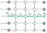
The network shown in Fig. 1(c) represents a bandpass filter with the so called in-line coupling topology, as illustrated in Fig. 2.
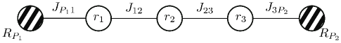
In this figure, white circles represent the resonators of the structure (), while dashed circles represent the terminal ports with reference impedances (, ). Also, solid lines connecting the circles represent the ideal admittance inverters of the network (, , ).
If Kirchhoff’s current law is applied to the nodes of the bandpass network shown in Fig. 1(c), the following linear system of equations is obtained
| (8) |
where is the admittance of the resonators, calculated as
| (9) |
Similarly as before, it is now convenient to express the matrix of the system as the sum of three matrices as
| (10) |
The first matrix is again the conductance matrix defined in (4). The second matrix is symmetric and contains the values of the admittance inverters of the network
| (11) |
Finally, the third matrix represents the admittances of the resonators
| (12) |
Note that the size of all these matrices is the same as that of the regular coupling matrix with ports, namely . Also, we want to remark that the admittance inverters are located in the off diagonal elements of (11), and that the information of the resonators appears in the diagonal entries of (12). We stress that all matrices involved in the formulation are symmetric, therefore assuring that the considered network is completely reciprocal.
III Network with Time Modulated Resonators
Applying time-varying signals to modulate the capacitors of the bandpass network shown in Fig. 1 makes the system non-linear [27, 28]. In this work, we will consider that the values of the capacitors are modulated in time with the following sinusoidal variation
| (13) |
where is the angular frequency of the modulating signal, is the initial phase, and is the modulation index. Even though we will use the same modulation frequency and modulation index to modulate all capacitors, their initial phases may be different along the network, i.e., with . It will be shown later in this paper that this phase difference is the key mechanism that enables non-reciprocal responses [24].
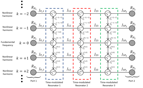
In this scenario, a number of nonlinear harmonics (or intermodulation products) are generated in each resonator, resulting into the equivalent network shown in Fig. 3.

These nonlinear harmonics are coupled by the time modulated capacitors. For simplicity, the figure only shows harmonics (i.e., with denoting the order of a given nonlinear harmonic).
The application of Kirchhoff’s current law on the network shown in Fig. 3 leads to a linear system with a structure very similar to the previous one given in (10). However, each entry in the matrix system becomes now a submatrix of size due to the generated nonlinear harmonics. In this way, the vector containing the nodal voltages becomes
| (14a) | ||||||
| (14b) | ||||||
where the number of harmonics considered is five (, ) and the total number of unknowns in the system of linear equations becomes . We recall that in our notation () is an integer sweeping the physical resonators (). Then () of (14b) are simply the to entries of () shown in (14a). Then, following the same strategy as before, the conductance matrix is written as
| (15) |
where () denotes the zero matrix. The other sub-matrices are diagonal and represent the loads to the new generated harmonics as and , with being the identity matrix. In addition, the matrix of the admittance inverters can now be written as
| (16) |
where the submatrices are also diagonal and represent the couplings of same order harmonics between the different resonators. Here we should remark that with the equivalent network employed, which uses ideal frequency independent inverters, the couplings of same order harmonics between different resonators are all identically affected by the original inverters. This is a narrowband approximation, usually introduced in the theory of coupling matrices [26]. In real implementations, harmonics will be affected by the inverters in a slightly different way, due to their intrinsic dispersive nature. These dispersive effects maybe important for wideband responses, and special techniques may be needed to preserve accuracy [29, 30]. However, for narrowband responses (fractional bandwidths typically less than 10%), the narrowband approximation usually gives good results [26].
Finally, the matrix that contains the resonator admittances becomes
| (17) |
Each admittance submatrix represents the coupling among the different nonlinear harmonics generated in a resonator with a time-modulated capacitor. In this paper we have used the theory reported in [31, 32] to model this non-linear behavior. Note that this theory is based on considering ideal capacitors. Applying the theory reported in [31, 32] permits to express each of these submatrices as
| (18) |
where is a diagonal matrix containing the angular frequencies of the nonlinear harmonics (spectral matrix), namely
| (19) |
The matrix includes the presence of the inductors in the modulated resonators and can be expressed as
| (20) |
Finally, models how the nonlinear harmonics are excited due to the modulated capacitors and it can be written as
| (21) |
The new elements of this matrix depend on the modulation index and on the phases of the modulating signal as
| (22) |
By doing straightforward operations with these matrices, the final admittance submatrix in (18) can be written as shown in (23) (top of the page).
| (23) |
In this last expression, we have employed the following auxiliary admittance
| (24) |
The form of the matrix shown in (23) admits an interesting interpretation of the non-linear phenomenon in terms of coupled network resonators. Following the coupling matrix formalism, the elements in the diagonal represent new resonators due to the generated nonlinear harmonics (we will call them harmonic resonators). Therefore, each physically modulated resonator gives rise to new harmonic resonators yielding to a network of order . These resonators have different resonant frequencies, transforming the original structure into an asynchronously tuned coupled resonators network.
The resonant frequencies of the new harmonic resonators can be obtained by equating the diagonal elements of the matrix shown in (23) to zero. However, following the coupling matrix formalism, it would be convenient to formulate all resonators to be equal, with additional frequency invariant susceptances to account for differences in the resonant frequencies. This can be accomplished by first writing (24) as
| (25) |
and then applying the following Taylor expansion
| (26) |
to the third term to obtain
| (27) |
Note that this Taylor expansion can be used in this context since, in general, we will assume: . This assumption is again related to the narrowband approximation assumed throughout the paper, and to the fact that to achieve good power conversion between non-linear harmonics, the modulation frequency should lay within the passband of the filter [24].
The comparison of this expression with (9) shows that the harmonic resonators can be made all equal to the static resonators in the unmodulated network. The differences in resonant frequencies can be modeled with additional frequency invariant susceptances, defined as
| (28) |
where, in order to make the frequency invariant susceptances truly independent on frequency, the center frequency of the passband has been used in the last definition. The approximation will remain valid for narrowband filters. These frequency invariant susceptances can also be formulated in terms of the initial lowpass capacitors as
| (29) |
It can be observed that the frequency invariant susceptances associated to harmonic resonators depend on the order of the nonlinear harmonic itself , on the modulation frequency and on the passband bandwidth. This expression is also very useful, since it will directly translate into the diagonal elements of the coupling matrix for the non-reciprocal filter by setting the lowpass capacitor to unity, i.e., .
It is illustrative to compare the structure of the matrices shown in (8) and in (23). Specifically, the off diagonal elements of the matrix (23) indicate that the new harmonic resonators are coupled following an in-line coupling topology among them. However, it can be observed that the matrix is not symmetric. This indicates that these harmonic resonators are coupled through non-reciprocal admittance inverters. Following this idea, we define a non-reciprocal admittance inverter to represent the coupling between two different harmonics and , belonging to a specific physical resonator , as
| (30) |
so a coupling from a lower order harmonic to an upper order harmonic will use the top formula of (30), while a coupling from an upper order harmonic to a lower order harmonic will involve the bottom formula. An explicit expression for this non-reciprocal inverter can be obtained in the lowpass domain as
| (31) |
where the center angular frequency of the passband has been used to define frequency invariant inverters.
Here we remark that these admittance inverters are different from those shown in (16). Admittance inverters in (16) come from the unmodulated network, and they couple same order harmonics between different physical resonators. On the contrary, these new admittance inverters play an important role in the non-linear process occurring within each time modulated resonator. As a consequence, the new admittance inverters in (31) model the couplings between the different harmonics, generated, due to the non-linear process, within the same physical resonator.
These last expressions indicate that the coupling between adjacent harmonic resonators belonging to a specific physical modulated capacitor can be controlled with the modulation frequency , modulation index , and initial phase of the modulation signal . Moreover, the degree of non-reciprocity of the coupling depends on both, the initial phase of the modulating signal and the modulation frequency. These expressions represent the values along the off-diagonal elements of the coupling matrix for the final non-reciprocal filter, once the value of the lowpass capacitor is set to unity ().
The analysis presented above permits an insightful interpretation of non-reciprocal filters in terms of an asynchronously tuned coupled resonators network. As already indicated, the order of the equivalent network is . Its coupling topology is further shown in Fig. 4. In this figure, harmonic resonators are identified with white circles as . These harmonic resonators are defined with the same inductors (), capacitors () and frequency invariant susceptances () as the original static resonators. However, the new frequency invariant susceptances () given in (29) must be added to correctly represent their resonant frequencies. Furthermore, solid lines represent regular inverters modeling the couplings of same order harmonics between different physical resonators, as defined in (6). Finally, lines terminated in arrows represent non-reciprocal inverters modeling the couplings between different order harmonic resonators belonging to the same physical resonator, as defined in (30) or (31). It is also interesting to note that this coupled resonator network can easily be characterized with the traditional coupling matrix formalism [26], using the results obtained in this Section. In this case the size of the coupling matrix is (.
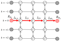
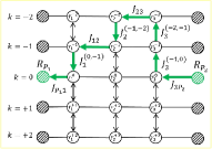
It is interesting to note that according to the admittance inverters expressed in (31), the coupling increases with the order of the harmonics. This implies that higher order harmonics will undergo very high couplings, which is a somewhat counter-intuitive scenario. The situation, however, can be explained with the coupling topology shown in Fig. 4. This topology explicitly states that couplings to higher harmonics can only occur from contiguous harmonics. Therefore, the power cannot be coupled from the fundamental frequency to harmonics of very high orders, with a very strong coupling.
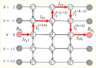
The topology shown in Fig. 4 explicitly shows that the non-reciprocal response in time-modulated filters originates due to the non-reciprocal coupling [see (31)] between adjacent nonlinear harmonics that appear in time-modulated resonators. Following this scheme, the underlying non-reciprocal mechanism can be intuitively understood as follows. Electromagnetic waves propagating from port can reach port and keep the same oscillation frequency by (i) going through the admittance inverters that link the different resonators at the fundamental frequency, as in regular in-line filters (see Fig. 2 and Fig. 5a); and (ii) going through an ideally infinite number of routes (assuming an infinite number of nonlinear harmonics) that appear in the topology due to the presence of harmonic resonators. One specific example of these routes, illustrated in Fig. 5b, involves the harmonic admittance inverters , , , and that impart a total phase of to the waves propagating therein. The output at port is then conformed by the interference of the waves coming from all possible routes. Let us now consider the dual case, i.e., waves coming from port and propagating towards port . As in our previous analysis, propagating waves can follow the path of common in-line filters (see Fig. 5c) plus potentially any of the ideally infinite routes enabled by harmonic resonators. The former leads to reciprocal contributions whereas any of the paths that encompasses nonlinear harmonics introduces non-reciprocity due to the non-reciprocal response of the impedance inverters. For instance, Fig. 5d shows the route previously analyzed but considering now the opposite propagation direction of the waves. This specific path involves the same harmonic impedance inverters as before, but traversed in the opposite direction, thus providing a total phase of to the waves (negative with respect to the previous scenario). For instance, assuming , the total phase difference between forward and backward paths in this example is of . It is thus evident that an adequate control of the phase imparted by each time-modulated resonator is key to control the response of this type of filters. At port , waves coming from all routes interfere to construct the output signal. Strong non-reciprocity at the same frequency arises due to the different wave interference that appears in ports and .
The design of time-modulated non-reciprocal filters can be carried out following the guidelines shown in [24]. In such design, the goal is to optimize the modulation frequency and index as well as the initial phase of the modulation signal applied to each resonator to (i) independently manipulate the interference of all waves that merge at ports and to boost non-reciprocity; (ii) maximize the energy coupled to nonlinear harmonics; and (iii) ensure that most energy is transferred back to the operation frequency at the device ports to minimize loss. It is important to remark that it is required to modulate at least two physical resonators to enable non-reciprocal responses [24]. If one modulates just a single resonator, the incoming energy will simply be distributed among various nonlinear harmonics that will then propagate through the network. Finally, note that we have focused on non-reciprocal responses at the same frequency. It is indeed possible to design devices based on time-modulated resonators that exhibit non-reciprocal responses between the fundamental frequency and any desired nonlinear harmonic. These devices will be governed by the topology shown in Fig. 4 and will follow the theory developed here.
IV Numerical Results
Using the coupling matrix formalism derived above, a software tool for the analysis of non-reciprocal in-line filters has been developed. In this Section, we will investigate the convergence of the numerical algorithm as a function of the number of harmonics included in the calculations.
The first example is a filter of order three whose unmodulated response has equal ripple return losses of dB. The filter coupling matrix yields
| (32) |
This coupling matrix gives the response of the normalized lowpass prototype. The bandpass response is adjusted to have a bandwidth of 47 MHz, with a center frequency of MHz (). By using the procedure shown in [24], the modulation parameters were optimized, leading to the following values: MHz, , and .
Here we should remark that the design of this filter is not yet completely determined by synthesis techniques. Rather, the coupling matrix shown in (32) gives the initial response of the unmodulated filter. Once this response is established, the parameters of the modulation signals are optimized to obtain the desired non-reciprocal response, using the procedure reported in [24].
In general, the design of this filter fully from synthesis techniques is very complex, and will involve (i) the calculation of suitable reflection and transmission polynomials to properly represent the desired (non-reciprocal) transfer functions, (ii) the extraction from these polynomials of a suitable coupling matrix and (iii) the transformation of the obtained coupling matrix into a form that represents the coupling topology shown in Fig. 4.
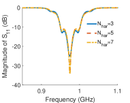
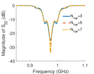
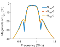
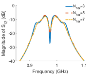
Fig. 6 shows the scattering parameters at the fundamental frequency, obtained for this filter with increasing number of harmonics . Here numerical results were obtained from the responses of the coupling matrices for the time modulated network. The coupling matrix is easily calculated starting with the coupling matrix given in (32) for the unmodulated network, and with the selected parameters for the modulation signal (, and ). Then, using the coupling topology shown in Fig. 4, the coupling matrix entries for the time modulated network are computed with (29) and (31) (with ). It can be observed that the results are in general very stable, showing only small differences as the number of harmonics is increased. Note that the algorithm converges using just harmonics and increasing further the number of harmonics leads to negligible changes in the simulated response. Results show that the filter has a passband which is quite flat in the forward direction with a bandwidth of MHz measured at the return loss level of dB. It should be stressed that, even though the network is non-reciprocal it is symmetric and thus return losses from both ports are identical. Insertion losses within the passband in the forward direction are dB. Since the network is lossless, these losses are in fact due to power that is converted to nonlinear harmonics and is not converted back to the fundamental frequency. A very strong non-reciprocity is obtained at the center of the passband, being the insertion loss of about dB. Overall, the insertion losses in the backward direction are greater that dB within the whole useful bandwidth. We observed in this case that fairly good isolation can be obtained at the center of the passband. However, the isolation deteriorates at the edges of the useful bandwidth. As explained in the previous section, the non-reciprocity is obtained by provoking energy conversion from the fundamental frequency to the generated non-linear harmonics. Although these conversion effects are non-reciprocal in magnitude and phase, the main mechanism that allows to obtain high non-reciprocity is the difference in phase between the forward and backward paths. Therefore, high isolation is obtained by adjusting the phases among the resonators to produce phase cancellation effects in the backward direction. With a small number of resonators (three in this example), these cancellation effects can be made efficient in a narrow bandwidth. Moreover, as it will be discussed in our next example, there is a trade-off between the isolation level and the bandwidth where this isolation is achieved. In general, larger isolation values can be obtained but only over a narrower bandwidth.
If we define the directivity between the forward and backward directions as
| (33) |
then a directivity of dB is obtained at center frequency. Moreover, the directivity within the useful passband is always better than dB.
To demonstrate the convergence of the algorithm when the order of the network is increased, we have also designed a fourth order non-reciprocal filter. For this second example the return losses of the unmodulated filter are dB, leading to the following coupling matrix
| (34) |
This time the bandpass response is adjusted to have a bandwidth of 58 MHz at a center frequency MHz, given a fractional bandwidth of . After optimization, the parameters of the modulated capacitors are MHz, , and .
Fig. 7 shows the simulated scattering parameters with increasing number of nonlinear harmonics . It is evident that the response is inaccurate if only three harmonics are included in the calculations. After increasing further the number of harmonics, the differences among the different simulations reduce considerably, especially for the reflection characteristic and the forward transmission coefficient. We have verified that including additional harmonics in the simulations leads to negligible variations in the simulated response, which indicates that good convergence is obtained with nine harmonics. As expected, this study shows that more harmonics needs to be used in the numerical simulations when the order of the network increases.
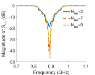

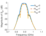
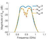
Moreover, it has been previously shown [16], that in this type of modulated resonators only the two first higher order harmonics are important in the non-linear process. Consequently, the minimum number of harmonics that need to be considered in the numerical simulations should grow, with the number of resonators in the network, according to the rule: . Note that the convergence results presented for the third and fourth order filters, shown in Fig. 6 and Fig. 7, are in agreement with this rule.
The filter shows an almost flat response for the transmission coefficient in the forward direction, having a bandwidth of MHz measured at a return loss of dB. The insertion losses in the forward direction are smaller than dB within the useful passband. Again, these losses correspond to power converted from the fundamental frequency into nonlinear harmonics that is not converted back into the fundamental frequency. The response of the filter shows a strong non-reciprocal behavior in the backward direction. Around the center frequency, the directivity is better than dB in a bandwidth of MHz. In the whole useful passband, the directivity is shown to be better than dB.
At this point it is interesting to observe that the optimum modulation frequency ( MHz) is slightly smaller than the bandwidth of the filter. This condition assures that the two first intermodulation products can be strongly excited, while the generation of higher order intermodulation products are minimized. Also, we emphasize that the response of the filter was optimized to achieve a good trade-off between the isolation level, and the bandwidth where it is achieved. Other optimization criteria are possible, for instance by increasing further the isolation level, at the expense of reducing the bandwidth where this isolation is achieved. For instance we have verified that by decreasing the frequency of the modulation signal to MHz, the directivity increases to dB, although in a narrow bandwidth of only MHz. In any case, this example shows that the proposed system offers high flexibility in the characteristics that can be achieved, that could be adapted to many different scenarios.
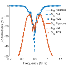
As validation of the theory presented in this paper, we employ this last filter design to compare our results with those obtained with the commercial tool ADS [33]. Here we remark that the ADS results were obtained using ideal built-in models to implement the time modulated capacitors through (13), combined with the large signal scattering parameters analysis module. In addition, we also check what is the impact of the approximations introduced in order to formulate the frequency independent elements required by the coupling matrix formalism. Essentially, the approximations involve (i) the representation of the harmonic resonators with the frequency invariant susceptances of (29), instead of using the rigorous admittances given in (24); and (ii) the use of frequency independent admittance inverters of (31), instead of the rigorous expressions shown in (30). Fig. 8 compares the filter response using these two different approaches, and using the commercial tool ADS. It can be observed that our theory (Rigorous) agrees perfectly with the results obtained with ADS. Small differences can be observed between these two results (ADS, Rigorous), and the results obtained introducing the approximations (CM). This indicates that the impact of the approximations introduced is indeed small, especially for narrowband filters.

V Practical Realization
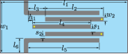
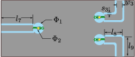
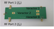
In this Section we present the fabrication and measurement of the two previously designed non-reciprocal filters, implemented in microstrip technology. Fig. 9 and Fig. 10 show the details of the filters together with pictures of the manufactured prototypes. It can be observed that the top metalization layer contains the input/output RF feeding lines and that the resonators are realized using quarter wavelength transmission lines terminated on one side with a via-hole connected to a varactor. On the bottom metalization layer, the ground plane of the microstrip line is modified to feed the various varactors (from Skyworks, model SMV1234) with the corresponding modulating signals using coplanar waveguides. In the figures we also show the positions where the varactors are soldered in the board. Note that a choke lumped inductor of value nH is incorporated to increase the isolation between the signals oscillating at and . It should be emphasized that this implementation enforces that the RF and modulating signals are supported on different planes of the substrates which significantly increases the isolation between them ( dB). The substrate material used for the fabrication is Rogers RT/duroid 6035 HTC with a relative dielectric constant and a thickness of mm. The final dimensions of the fabricated prototypes are collected in Table I and Table II for the third and fourth order filters, respectively.

| 50 | 3.44 | 3 | 2.66 | 0.36 | 0.22 | 11.3 | 153 | 72 |
| 31.3 | 69 | 100 | 17 | 31.95 | 15.5 | 20.4 | 1.8 | 1 |
| 70 | 4.56 | 2.21 | 0.21 | 9.3 | 160 | 73 | 27.8 |
| 70.3 | 98.1 | 23.4 | 22.5 | 14 | 17 | 25.5 | 26.9 |
Fig. 11a shows the measured results for the third order filter in the absence of any modulation and compares them with the simulated response using the coupling matrix formalism. Here we should remark that the simulated responses of the filters are all obtained with the theoretical analysis presented in Section III. In addition, it can be observed in the measured response some deviations with respect to the response of the designed prototype shown in Fig. 6. The differences are mainly due to the insertion losses within the passband, which are around dB, and to some parasitic cross couplings that were not taken into account during the initial design. These two factors have been included in the simulated responses obtained with the coupling matrix formalism derived in this work, shown in Fig. 11. Losses in the resonators are modeled with an additional resistor connected in parallel. The response show in Fig. 11a is used to extract the unloaded quality factors of the resonators, giving . This unloaded quality factor is small, but it is not uncommon of planar technology [34], and especially when using microstrip line printed resonators. In addition, we have found that the drop of selectivity in the lower side of the passband is mainly due to a non negligible cross coupling between the ports and the second resonator, giving normalized coupling factors or . Although of much weaker value, there is also a small parasitic coupling between the first and third resonator, which is modeled with a normalized coupling factor of . It can be observed that the agreement between measured and simulated results are reasonably good, once losses and parasitic couplings are included in the derived coupling matrix formalism.
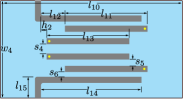

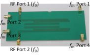
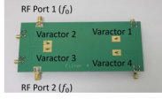
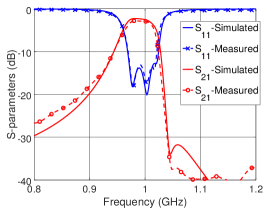
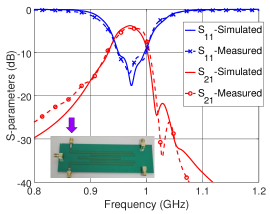
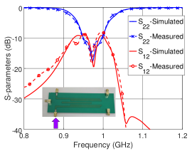
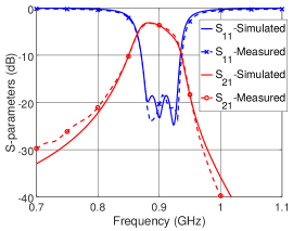
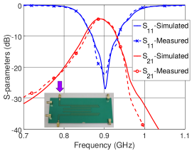
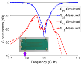
Fig. 11b presents the measured versus simulated results when the modulating signal is applied to the varactors and the filter is excited from the first port. It can be observed that the filter behaves as in the unmodulated case, with increased losses of around dB that account for both dissipation effects and the power converted into nonlinear harmonics. The useful bandwidth measured at a return loss level of dB is MHz. Fig. 11c shows the response of the prototype when it is excited from the second port. The filtering response is suppressed and instead the device behaves as an isolator that attenuates all incoming power. Maximum non-reciprocity is achieved at the center of the passband with a directivity of dB. It can be observed that when losses and parasitic cross couplings are included in the coupling matrix model, a good agreement is maintained between measured data and numerical simulations.
Measurements corresponding to the fourth order filter are shown in Fig. 12. Fig. 12a plots the response of the filter before introducing the modulating signal and compares it with respect to the response of the ideal circuit. Again the bandwidth and the ripple level obtained within the passband are very similar. Measured results exhibit a perfectly constant equi-ripple response, since the resonant frequencies of the resonators are slightly tuned with constant voltages applied to the varactors. The insertion losses due to dissipation effects in the resonators and in the varactors are slightly larger than in the previous filter, obtaining a minimum level of dB that slowly increases towards the end of the passband. The insertion losses measured in the unmodulated case (Fig. 12a) were used again to extract the unloaded quality factor of the resonators, obtaining essentially the same value as in the previous example. This is something to be expected, since the same resonators as before were used in this second prototype, and the same technology was used for manufacturing. In any case, this also shows high repeatability of the employed manufacturing process.
Measured results again show a drop in selectivity as compared to the designed response of Fig. 7, especially in the lower side of the passband. Once more we found that this is due to parasitic cross couplings not taken into account during the initial design process. In the comparison shown in Fig. 12, we can observe good agreement between measured and simulated responses when losses and parasitic couplings are included in the derived model. Again, we found that the strongest parasitic couplings occur between the ports and the closest non contiguous resonators: and . However, non negligible parasitic couplings have also been found between internal resonators: and .
| (dB) | (dB) | (dB) | (%) | |
|---|---|---|---|---|
| Third order | 4.5 | 11 | 13.8 | 4.6 |
| Fourth order | 4.4 | 11 | 13.6 | 6.4 |
Fig. 12b presents the measured results obtained from the manufactured prototype when the modulating signal is applied to the varactors and the filter is excited from the first port. The fabricated prototype behaves as a filter with a useful bandwidth of MHz measured at a return loss level of dB. With respect to the unmodulated case, the insertion losses in the forward direction have increased to dB. As in the previous case, the extra losses are due to power converted into nonlinear harmonics that is not converted back to the fundamental frequency. Exciting the device from the second port significantly attenuates the propagating energy. The strong non-reciprocity predicted by the initial simulations is confirmed by the measurements. Around the center frequency of the passband, the directivity is better than dB in a bandwidth of MHz. Across the entire passband, the directivity is always better than dB. In general, good agreement between measured and simulated responses are obtained when losses and parasitic couplings are included in the derived coupling matrix model. For reference, the basic performances for both manufactured filters are collected in Table III.
Another important characteristic of these devices for many applications is the power handling levels. The hardware built could not be tested under high power signals. Primarily, the power handling will be limited by the technology used to build a similar unmodulated circuit [35]. However, an interesting future research topic will be the assessment on how the additional circuitry needed by modulation signals and the presence of varactors affect the power handling levels, and which arrangements are more appropriate to reduce these undesired effects.
VI Conclusion
We have presented the analysis of non-reciprocal filters based on time modulated capacitors using a coupling matrix formalism. From the initial topology of the filter, a novel coupling topology using harmonic resonators is first derived. Closed form analytic expressions have been obtained to represent the harmonic resonators with frequency invariant susceptances, thus obtaining the diagonal elements of the traditional coupling matrix. Also, non-reciprocal admittance inverters have been analytically computed to account for the couplings between harmonic resonators, thus obtaining the off-diagonal elements of the coupling matrix. The derived analysis method has been validated with the design and fabrication of third and fourth order filters implemented in microstrip technology. Measured results on the fabricated prototypes, and results obtained with a commercial tool are found to agree well with respect to numerical calculations obtained using the new coupling matrix formulation, thus fully validating the theory presented.
Acknowledgment
Authors are grateful to Rogers Corporation for the generous donation of the dielectrics employed in this work.
References
- [1] D. M. Pozar, Microwave Engineering. John Wiley and Sons, 1998, ISBN: 0-471-17096-8.
- [2] C. Caloz, A. Alu, S. Tretyakov, D. Sounas, K. Achouri, and Z. L. Deck-Leger, “Electromagnetic nonreciprocity,” Phys. Rev. Appl., vol. 10, no. 4, p. 047001, 2018.
- [3] A. Kord, D. L. Sounas, and A. Alu, “Achieving full-duplex communication: Magnetless parametric circulators for full-duplex communication systems,” IEEE Microw. Mag., vol. 19, no. 1, pp. 84–90, Janaury 2018.
- [4] T. Kodera, D. L. Sounas, and C. Caloz, “Magnetless nonreciprocal metamaterial (mnm) technology: Application to microwave components,” IEEE Trans. Microw. Theory Techn., vol. 61, no. 3, pp. 1030–1042, March 2013.
- [5] R. Fleury, D. L. Sounas, C. F. Sieck, M. R. Haberman, and A. Alu, “Sound isolation and giant linear nonreciprocity in a compact acoustic circulator,” Science, vol. 343, no. 6170, pp. 516–519, 2014.
- [6] N. A. Estep, D. L. Sounas, J. Soric, and A. Alu, “Magnetic-free non-reciprocity and isolation based on parametrically modulated coupled resonator loops,” Nat. Phys., vol. 10, no. 12, pp. 923–927, December 2014.
- [7] N. A. Estep, D. L. Sounas, and A. Alu, “Magnetless microwave circulators based on spatiotemporally modulated rings of coupled resonators,” IEEE Trans. Microw. Theory Techn., vol. 64, no. 2, pp. 502–518, February 2016.
- [8] N. Reiskarimian and H. Krishnaswamy, “Magnetic-free non-reciprocity based on staggered commutation,” Nat. Commun., vol. 7, no. 4, p. 11217, April 2016.
- [9] N. Reiskarimian, J. Zhou, and H. Krishnaswamy, “A cmos passive lptv nonmagnetic circulator and its application in a full-duplex receiver,” Nat. Commun., vol. 52, no. 5, pp. 1358–1372, May 2017.
- [10] T. Dinc, M. Tymchenko, A. Nagulu, D. Sounas, A. Alu, and H. Krishnaswamy, “Synchronized conductivity modulation to realize broadband lossless magnetic-free non-reciprocity,” Nat. Commun., vol. 8, p. 759, October 2017.
- [11] A. Kord, D. L. Sounas, and A. Alu, “Magnet-less circulators based on spatiotemporal modulation of bandstop filters in a delta topology,” IEEE Trans. Microw. Theory Techn., vol. 66, no. 2, pp. 911–926, February 2018.
- [12] ——, “Pseudo-linear time-invariant magnetless circulators based on differential spatiotemporal modulation of resonant junctions,” IEEE Trans. Microw. Theory Techn., vol. 66, no. 6, pp. 2731–2745, June 2018.
- [13] Y. Yu, G. Michetti, A. Kord, D. Sounas, F. V. Pop, M. P. P. Kulik, Z. Qian, A. Alu, and M. Rinaldi, “Magnetic-free radio frequency circulator based on spatiotemporal commutation of mems resonators,” in IEEE Microelectromech. Syst., January 2018, pp. 154–157.
- [14] Z. Yu and S. Fan, “Complete optical isolation created by indirect interband photonic transitions,” Nat. Photonics, vol. 3, p. 91, January 2008.
- [15] H. Lira, Z. Yu, S. Fan, and M. Lipson, “Electrically driven nonreciprocity induced by interband photonic transition on a silicon chip,” Phys. Rev. Lett., vol. 109, p. 033901, July 2012.
- [16] S. Qin, Q. Xu, and Y. E. Wang, “Nonreciprocal components with distributedly modulated capacitors,” IEEE Trans. Microw. Theory Techn., vol. 62, no. 10, pp. 2260–2272, October 2014.
- [17] J. Chang, J. Kao, Y. Lin, and H. Wang, “Design and analysis of 24-ghz active isolator and quasi-circulator,” IEEE Trans. Microw. Theory Techn., vol. 63, no. 8, pp. 2638–2649, August 2015.
- [18] M. M. Biedka, R. Zhu, Q. M. Xu, and Y. E. Wang, “Ultra-wide band non-reciprocity through sequentially-switched delay lines,” Scientific Reports, vol. 7, p. 40014, January 2017.
- [19] D. Correas-Serrano, A. Alu, and J. S. Gomez-Diaz, “Magnetic-free nonreciprocal photonic platform based on time-modulated graphene capacitors,” Phys. Rev. B, vol. 8, p. 165428, 2018.
- [20] D. L. Sounas, J. Soric, and A. Alu, “Broadband passive isolators based on coupled nonlinear resonances,” Nat. Electron., vol. 1, pp. 113–119, February 2018.
- [21] D. C. Serrano, J. G. Diaz, D. Sounas, Y. Hadad, A. A. Melcon, and A. Alu, “Non-reciprocal graphene devices and antennas based on spatio-temporal modulation,” IEEE Antennas Wireless Propag. Lett., vol. 15, no. 6, pp. 1529–1533, June 2016.
- [22] T. Kodera, D. L. Sounas, and C. Caloz, “Breaking temporal symmetries for emission and absorption,” Proc. Natl. Acad. Sci., vol. 113, p. 3471, 2016.
- [23] S. Taravati and C. Caloz, “Mixer-duplexer-antenna leaky-wave system based on periodic space-time modulation,” IEEE Trans. Antennas Propag., vol. 65, no. 2, pp. 442–452, February 2017.
- [24] X. Wu, X. Liu, M. D. Hickle, D. Peroulis, J. S. Gomez-Diaz, and A. A. Melcon, “Isolating bandpass filters using time-modulated resonators,” IEEE Trans. Microw. Theory Techn., vol. Submitted, October 2018.
- [25] R. J. Cameron, “Advanced coupling matrix synthesis techniques for microwave filters,” IEEE Trans. Microw. Theory Techn., vol. 51, no. 1, pp. 1–10, Jan. 2003.
- [26] R. J. Cameron, C. M. Kudsia, and R. R. Mansour, Microwave Filters for Communication Systems. Hoboken, New Jersey: Wiley, 2007, ISBN: 978-0-471-45022-1.
- [27] L. A. Pipes, “Matrix analysis of linear time-varying circuits,” J. of Appl. Phys., vol. 25, no. 9, pp. 1179–1185, September 1952.
- [28] K. D. Dikshit, “An analysis of time-varying circuits,” Int. J. of Electron., vol. 35, no. 4, pp. 453–460, April 1873.
- [29] P. Soto, E. Tarin, V. Boria, C. Vicente, J. Gil, and B. Gimeno, “Accurate synthesis and design of wideband inhomogeneous inductive waveguide filters,” IEEE Trans. Microw. Theory Techn., vol. 58, no. 8, pp. 2220–2230, August 2010.
- [30] F. M. Vannin, D. Schmitt, and R. Levy, “Dimensional synthesis for wide-band waveguide filters and diplexers,” IEEE Trans. Microw. Theory Techn., vol. 52, no. 11, pp. 2488–2495, November 2004.
- [31] S. Darlington, “Linear time-varying circuits - matrix manipulations, power relations, and some bounds on stability,” The Bell System Technical Journal, vol. 42, no. 6, pp. 2575–2608, November 1963.
- [32] C. F. Kurth, “Steady-state analysis of sinusoidal time-variant networks applied to equivalent circuits for transmission networks,” IEEE Trans. Circuits Syst., vol. CAS-24, no. 11, pp. 610–624, November 1977.
- [33] Keysight Technologies, ADS - Advanced Design System, EEsof, Santa Rosa, CA, USA, 2019. [Online]. Available: https://www.keysight.com
- [34] Y.-Y. Zhu, Y.-L. Li, and J.-X. Chen, “A novel dielectric strip resonator filter,” IEEE Microw. Wireless Compon. Lett., vol. 7, pp. 591–593, July 2018.
- [35] L.-S. Wu, X.-L. Zhou, W.-Y. Yin, M. Tang, and L. Zhou, “Characterization of average power handling capability of bandpass filters using planar half-wavelength microstrip resonators,” IEEE Microw. Wireless Compon. Lett., vol. 19, no. 11, pp. 686–688, November 2009.