Two-dimensional transition metal chalcogenides with hexagonal and orthorhombic structures: candidates for auxetics and photocatalysts
Abstract
In this paper, we perform theoretical study on the physical properties of two-dimensional transition metal chalcogenides MX2 and M2X3 (M= Ni, Pd; X= S, Se, Te). These studied materials are classified in three stable phases according to their lattice structures: hexagonal MX2, orthorhombic MX2 and orthorhombic M2X3. They have either isotropic or anisotropic in-plane properties depending on their symmetries. In particular, the orthorhombic MX2 and M2X3 have low lattice symmetry and present highly anisotropic properties. The orthorhombic MX2 possess giant negative in-plane Poisson’s ratios, different from the other two phases. Moreover, by joint analysis of band gap, band edge and optical absorption, the orthorhombic MX2 and M2X3 are found to be highly efficient as water splitting photocatalysts within the visible and ultraviolet sunlight regions.
PACS numbers: 62.20.Dc, 63.20.dk, 85.30.De
I INTRODUCTION
Two-dimensional (2D) group-VIII transition metal chalcogenides (TMCs), including the transition metal dichalcogenides (for example, MoS2, MoSe2, WS2 and WSe2, etc.) have presented great potentials in electronic and optical devices, such as high current on/off ratio field-effect transistors (FETs) Radisavljevic et al. (2011); Wang et al. (2012), photodetectors Lopez-Sanchez et al. (2013); Koppens et al. (2014) and valleytronic applications Mak et al. (2012); Zeng et al. (2012). Most reported 2D TMCs have isotropic mechanical and electronic properties due to their highly symmetric structures. The symmetry of lattice structure indeed plays a vital role in determining the electronic properties of materials. By lowering the symmetry of the structure, it is possible to induce strong in-plane anisotropic properties in 2D materials, as observed in puckered phosphorene Li et al. (2014); Qiao et al. (2014) and group-IV monochalcogenides (SnS, SnSe, GeS, GeSe) Gomes and Carvalho (2015); Hanakata et al. (2016); Xu et al. (2017). As have already been reported, the anisotropic properties have the advantage for certain applications, such as polarized light detection devices and valleytronics Tian et al. (2016); Kou et al. (2015); Wang et al. (2015).
Recently, few-layer PdSe2 has been successfully synthesized via mechanical exfoliation and selenization on the precursor Pd layer Li et al. (2018); Chow et al. (2017); Zeng et al. (2019), which has aroused great interests due to its ambient stability, high carrier mobility (158 cm2V-1s-1) and in-plane anisotropic properties Oyedele et al. (2017). In contrast to its hexagonal phase (Fig.1(b)), the synthesized few-layer PdSe2 forms an orthorhombic lattice with puckered pentagonal structure as illustrated in Fig. 1(c). Moreover, Li revealed a much lower diffusion barrier of Se vacancies in PdSe2 than that of S vacancy in MoS2 Nguyen et al. (2018). Further, Lin . demonstrated that the introduction of Se vacancy in few-layer PdSe2 can enhance the interlayer interaction and decrease the Se/Pd element ratio, which creates a new structure phase, , Pd2Se3 Lin et al. (2017), as shown in Fig. 1(d). It is therefore highly desired to look for other 2D TMCs with a similar structure as PdSe2 or Pd2Se3, which may be stable and reveal the in-plane anisotropic properties.
Furthermore, one important application of 2D materials is the photocatalytic water splitting, , to convert solar energy into chemical energy without additional cost Iwase et al. (2011); Maeda and Domen (2010); Wang et al. (2008). Since the discovery of TiO2 as a photocatalyst in 1972 Fujishima and Honda (1972), more and more semiconductors have been proposed, including 2D semiconductors such as g-C3N4 and MoS2 Lu et al. (2016); Zhang et al. (2012). Particularly, one or few-layers 2D semiconductors are indeed thin, with inherent merit as photocatalysts due to their extremely large specific surface area. In fact, an ideal photocatalyst should have two characters: (i) the band edge need to straddle both the reduction potential of H2/H+ (-4.44 eV at pH=0) and the oxidation potential of H2O/O2 (-5.67 eV at pH=0); (ii) an appropriate optical gap to guarantee the absorption of the solar light. Once satisfying the principle (i), the holes and electrons can drive both the oxidation and reduction reactions to generate O2 and H2 from aqueous solution. We will use these principles to look for possible photocatalysts from the 2D TMCs studied in this paper.
In this paper, we will perform systematic study on 2D TMCs based on the VIII-VIA compounds in the form of MmXn, where M refers to the elements Ni and Pd, and X represents S, Se and Te. We will calculate the physical properties of eighteen 2D TMCs from first principles by using density functional theory (DFT). The structures of these materials are classified in three phases, namely, the hexagonal MX2 (H-MX2), the orthorhombic MX2 (O-MX2) and the orthorhombic M2X3 (O-M2X3). In the following, We will first present the details of the numerical methods in Sec. II and show the main results in Sec. III, including stability, mechanical, electronic and optical properties of monolayer MmXn, and their potential applications in photocatalyst. Finally, we summarize our major findings In Sec. IV.
II CALCULATION METHOD
The electronic properties of TMCs are calculated from first-principles by using DFT as implemented in VASP code Kresse and Furthmüller (1996). The Perdew-Burke-Ernzerhof (PBE) parametrized generalized gradient approximation (GGA) and projected augmented wave (PAW) are adopted to describe exchange correlation potential and ion-electron interactionBlöchl (1994); Perdew et al. (1996). The kinetic energy cutoff and -point mesh of Brillouin zone (BZ) are set to 500 eV and 15151 Monkhorst and Pack (1976), respectively. A vacuum thickness of 20 Å is added to avoid the periodic interaction. Moreover, the energy convergence criteria and stress forces are set to 10-5 eV and 0.01 eV/Å, respectively. For few-layer TMCs, the van der Waals (vdW) force is corrected by using a semi-empirical DFT-D2 method Grimme (2006); Kerber et al. (2008). The spin-orbit coupling (SOC) is added into self-consistent calculations. Also, the corrected band structures are calculated by adopting hybrid Heyd-Scuseria-Ernzerhof (HSE06) method Heyd et al. (2005).
The thermal stability of monolayer TMCs is evaluated by using PHONOPY code based on density functional perturbation theory (DFPT) and finite difference method Gonze et al. (1994); Gonze and Lee (1997); Giannozzi et al. (1991). We construct a 33 supercell and adopt 551 -point mesh to obtain force constants and phonon spectrum. In order to eliminate the imaginary frequency, the highly accurate energy convergence criteria and stress forces are set to 10-8 eV and 10-4 eV/Å, respectively.
III RESULTS AND DISCUSSIONS
III.1 Structural stability
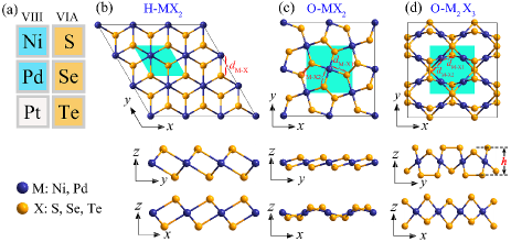
We firstly study the basic geometric structures and thermal stability of monolayer MmXn (M= Ni, Pd; X= S, Se, Te). After fully optimizing the atomic positions, the MmXn stabilizes into three structural symmetries as shown in Fig. 1, namely, the hexagonal H-MX2, the orthorhombic O-MX2, and the orthorhombic O-M2X3. All geometric structures are built up with three atomic layers as X-M-X, in which one M layer is sandwiched with two X layers. Each M atom binds six X atoms in H-MX2 and four X atoms in O-MX2 and O-M2X3. Detailed geometry analysis show that the space groups of H-MX2, O-MX2 and O-M2X3 are 31 (No. 164), 21/ (No. 14) and (No. 59), respectively. In contrast to the common phase of hexagonal H-MX2, the space groups of O-MX2 and O-M2X3 have much lower symmetry.
The relaxed structural parameters, such as lattice constants ( and ), bond lengths (), and vertical heights () are listed in Table 1. These results show clearly that when the atomic radius of element M (X) increases from Ni (S) to Pd (Te), all bond lengths within the same structural phase always increase. Comparing to the hexagonal structure of H-MX2, the bond lengths in two orthorhombic O-MX2 and O-M2X3 are more close to each other, but the height, defined as the out of plane distance between the top and bottom X sub-layers, are totally different. Furthermore, for O-MX2 and O-M2X3 phases, there are diversity of in-plane lattice constants along different crystal lines, originating from the bond length difference between and , as illustrated in Fig. 1. These differences break further the geometry symmetry and induce subsequently anisotropic mechanical and optical properties, as we will explore in detail in the following.
| (Å) | (Å) | (Å) | (eV) | (eV) | ||
|---|---|---|---|---|---|---|
| H-NiS2 | 3.348 | 3.348 | 2.258 | 2.330 | 0.61 | 1.10 |
| H-NiSe2 | 3.547 | 3.547 | 2.390 | 2.467 | 0.21 | 0.58 |
| H-NiTe2 | 3.787 | 3.787 | 2.576 | 2.721 | 0 | 0 |
| H-PdS2 | 3.548 | 3.548 | 2.395 | 2.480 | 1.27 | 1.80 |
| H-PdSe2 | 3.730 | 3.730 | 2.523 | 2.627 | 0.72 | 1.13 |
| H-PdTe2 | 4.026 | 4.026 | 2.701 | 2.756 | 0.26 | 0.52 |
| O-NiS2 | 5.215 | 5.326 | 2.172/2.182 | 1.149 | 0.82 | 2.40 |
| O-NiSe2 | 5.512 | 5.702 | 2.305/2.314 | 1.368 | 1.02 | 2.27 |
| O-NiTe2 | 5.955 | 6.261 | 2.489/2.498 | 1.552 | 0.95 | 1.89 |
| O-PdS2 | 5.472 | 5.571 | 2.328/2.339 | 1.267 | 1.18 | 2.14 |
| O-PdSe2 | 5.744 | 5.919 | 2.452/2.462 | 1.488 | 1.36 | 2.16 |
| O-PdTe2 | 6.146 | 6.439 | 2.625/2.631 | 1.693 | 1.27 | 1.90 |
| O-Ni2S3 | 5.239 | 5.57 | 2.190/2.256 | 3.438 | 0.38 | 1.77 |
| O-Ni2Se3 | 5.423 | 5.926 | 2.310/2.383 | 3.704 | 0.37 | 1.61 |
| O-Ni2Te3 | 5.499 | 6.737 | 2.488/2.571 | 4.105 | 0.30 | 1.05 |
| O-Pd2S3 | 5.773 | 5.907 | 2.341/2.427 | 3.582 | 0.45 | 1.50 |
| O-Pd2Se3 | 5.976 | 6.114 | 2.455/2.539 | 3.842 | 0.42 | 1.39 |
| O-Pd2Te3 | 6.122 | 6.608 | 2.622/2.696 | 4.228 | 0.60 | 1.24 |
The thermal stability of O-MX2 and O-M2X3 is qualitatively examined by ab initio molecular dynamics simulations implemented in GULP Gale and Rohl (2003); Gale (1997). Here we skip the discussion of H-MX2, as these common hexagonal structures have already been synthesized successfully Zhou et al. (2018); Shao et al. (2017); Miró et al. (2014). In our stability analysis, the 33 supercell of monolayer TMCs is used, the time interval and time step of the testing period are set to be 510-12 s and 110-15 s, respectively. Our results show that the total energy of each structure considered in the O-MX2 and O-M2X3 phases is oscillating persistently around a fixed value during the whole simulation (see the data of 300K presented in Fig. S1 and S2 of Supplementary Information). The stability of these structures is further conformed from the spectra of phonon dispersions shown in Fig. S3 and Fig. S4 of Supplementary Information. No negative acoustic branch is observed for all the structures considered in this paper. These results obtained from ab initio molecular dynamics simulations and phonon dispersions from first-principles indicate that the monolayer O-MX2 and O-M2X3 with M= Ni, Pd and X= S, Se, Te are all stable at room temperature. We will then continue the study by examining their mechanical and electronic properties, together with the phase of H-MX2.
III.2 Mechanical properties
Three phases of monolayer TMCs considered in this paper present totally different lattice structures. Materials belonging to the same phase of TMCs may have similar properties originating from the characters of their space group, but these from different phases should have significant differences in their physical properties. As one of the most important mechanical properties, we exam first Young’s modulus and Poisson’s ratio in the following.
Based on Hooke’s law, the relationship between stiffness constants and modulus is given by
| (1) |
where the in-plane stiffness tensor (,=1,2,6) is equal to the second partial derivative of strain energy , which is obtained by
| (2) |
where the tensile strain is defined as =(-)/, here and are strained and unstrained lattice constants, respectively. Young’s modulus and Poisson’s ratio can be expressed as functions of the in-plane stiffness tensors asZhong et al. (2018)
| (3) |
| (4) |
In fact, the anisotropic mechanical feature can be further checked by calculating the orientation-dependent Young’s modulus and Poisson’s ratio , which can be expressed as Wang and Geng (2017)
| (5) |
| (6) |
where s=sin and c=cos.
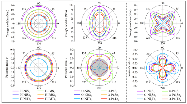
The in-plane stiffness tensors are obtained from a series of strain 2% and a step of 0.5%. All in-plane stiffness tensors fitting from Eq. (2) for eighteen monolayer TMCs are collected in Table S1 of Supplementary Information. The orientation-dependent Young’s modulus and Poisson’s ratio calculated by using Eq. (5) and (6) are plotted in Fig. 2. It is clear that all structures in the H-MX2 phase are isotropic as both Young’s modulus and Poisson’s ratio keep as constants when varying ; but the other two phases, O-MX2 and O-M2X3, are highly anisotropic with clear angle-dependent mechanical properties.
Particularly, Young’s modulus of O-MX2 phase increase monotonically from a minimum Young’s modulus along direction (=0∘) to a maximum value along direction (=90∘). However, the maximum and minimum values of O-M2X3 phase are located at 45∘ and 0∘ (90∘), respectively. For the same element M (, Ni, Pd), Young’s modulus decreases as X changes from S to Te due to the increment of the M-X bond strength. Furthermore, our calculations show that O-Ni2Te3 and O-Pd2Te3 have ultra-low Young’s modulus ( 20 N/m), which are even lower than monolayer graphene (340 N/m) and MoS2 (125 N/m)Lee et al. (2008); Çakır et al. (2014), indicating their enormous potential in flexible devices.
For Poisson’s ratio, besides the quite interesting anisotropic feather appeared in O-MX2 and O-M2X3, our calculations show that three monolayer TMCs, O-NiSe2, O-NiTe2 and O-PdTe2, present negative Poisson’s ratios. The absolute value of negative Poisson’s ratio obtained among these materials is -0.228 in O-NiTe2 along 56∘ to the axis (see Fig. 1(c)). A material with negative Poisson’s ratio exhibits an interesting auxetic effect, , it expands along one direction if stretched along another direction. Auxetic materials are highly desirable for tissue engineering, bulletproof vests and many other medical applications. As a comparison to existing auxetic 2D materials such as borophene, penta-graphene, tinselenidene, etc., we collect and list their Poisson’s ratios together with current values of O-NiSe2, O-NiTe2 and O-PdTe2 in Table 2. O-NiTe2 has lowest Poisson’s ratio among three studied materials, which is comparable to other reported auxetic 2D materials.
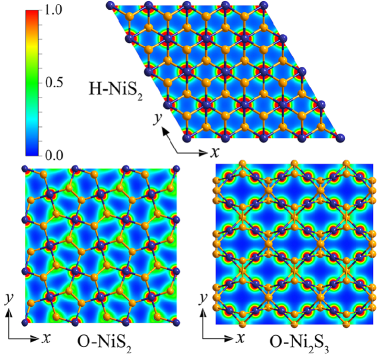
Actually, the nature of isotropic or anisotropic mechanical properties can be explained by analyzing the charge densities obtained from first principles. Here we use the case of M=Ni and X=S as an example to compare the charge distributions in three different structural phases. As plotted in Fig. 3, the charge densities of H-NiS2 are localized isotropically around Ni atoms. On the contrary, the charge densities of O-NiS2 and O-Ni2S3 are not uniformly distributed, but form patterns continuing along one crystal line. To be more precisely, for O-NiS2, the extended pattern is along direction, and for O-Ni2S3, it is along the diagonal direction. This is, indeed, consistent with the calculated Young’s modulus, in which the maximum value appear along the continuous pattern. The electron orbitals are hybridized stronger along these directions, leading to larger overlap of wave functions and larger bonding strength, and subsequently higher stiffness.
| System | |||
|---|---|---|---|
| O-NiSe2 | -0.018 | -0.036 | -0.050 |
| O-NiTe2 | -0.037 | -0.100 | -0.228 |
| O-PdTe2 | -0.001 | -0.002 | -0.058 |
| Borophene Zhong et al. (2018) | -0.022 | -0.009 | - |
| -Silica Gao et al. (2017) | -0.123 | -0.112 | - |
| Penta-graphene Zhang et al. (2015) | -0.068 | -0.068 | - |
| Be5C2 Wang et al. (2016) | -0.041 | -0.16 | - |
| -AsN Xiao et al. (2018) | -0.177 | -0.068 | -0.296 |
| Tinselenidene Zhang et al. (2016) | -0.171 | 0.46 | - |
III.3 Electronic properties
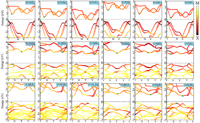
In this section, we study the electronic properties of monolayer TMCs. We firstly perform band structure calculations by using PBE. The results show that most materials considered in our paper are semiconductors (see details in Supplementary Information). As the PBE method usually underestimates the band gap of a semiconductor, we performed DFT calculations in VASP with more accurate HSE06 method and show the obtained band structures with projected densities in Fig. 4. The HSE06 results are similar as those in PBE, and all monolayer TMCs are semiconductors with indirect band gaps, except H-NiTe2 which is a metal. Detailed analysis shows that, for H-MX2 phase, the conduction band minimum (CBM) and the valence band maximum (VBM) are mainly attributed from element X; for O-MX2 and O-M2X3 phases, the CBM and VBM originate from both compounds of M and X. The values of band gap obtained from both PBE and HSE06 are listed in Table 1. It indicates that for the materials in the same structural phase, the band gaps always decrease as the element X varies from S to Te, which are similar to those observed in MoX2 and WX2 (X=S, Se and Te) Kang et al. (2013). As there are relatively heavy elements in the considered TMCs, it is worth checking also the effects of the SOC. From the results obtained with or without SOC in PBE (see details in Supplementary Information), the SOC interaction is overall negligible for most materials considered in our paper, except H-PdSe2 and H-PdTe2. In these two materials, there are large splittings of energy bands due to SOC, especially around the points. However, these splitting will not change qualitatively the properties we are interested in (see details in Fig. S7), therefore we will mainly show results without SOC in the following.
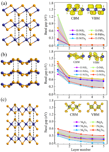
All three phases of TMCs present stable multilayer structures stacked along the direction perpendicular to their plane. In Fig. 5(a), we show atomic structures of stacked trilayer TMCs. The stacking sequence of H-MX2, O-MX2 and O-M2X3 is AAA stacking. We calculate further the electronic properties of multilayer TMCs by using relaxed structures as shown in Fig. 5(a), and present the main results in Fig. 5(b). Here, we consider mainly the thickness-dependence of the electronic properties of multilayer structure, and show the values of band gap with different number of layers ranging from 1 to 5. As is well known, the interlayer vdW interaction, which is absent in a monolayer, plays a vital role to determine the properties of multilayer 2D materials, especially at low energy around the Fermi level. In general, the interlayer vdW interaction will lower the band gap for semiconducting 2D materials, because of the hybridization of the bands between neighboring layers. This is indeed also the case for TMCs considered in our paper. In particular, once H-MX2 becomes a bilayer, its band gap promptly decreases to zero (see the results shown in Fig. S8), indicating that it gives a fierce response to the thickness. For O-MX2 and O-M2X3 phases, their band gaps keep decreasing when adding more layers, but slowly. Specifically, the variation ranges of band gaps are 0 1.27 eV, 0.26 1.36 eV and 0 0.60 eV for H-MX2, O-MX2 and O-M2X3, respectively. To further explore the origin of the relationship between the band gaps and the interlayer coupling, Fig. 5 shows the band decomposed charge densities of CBM and VBM in the monolayer. For H-NiS2, O-NiS2 and O-Ni2S3, charge densities of CBM and VBM are distributed among outside S atoms, Ni-S bonds and inside Ni atoms, respectively. When the monolayers are stacked together, the few-layer H-NiS2 and O-Ni2S3 have maximum (minimum) interlayer charge overlapping, leading to maximum (minimum) change of band gap.
III.4 Photocatalyst and light absorption
Most monolayer TMCs considered in this paper are semiconducting with energy gaps ranging from 0.52 to 2.40 eV according to HSE06 calculations, providing a wide range of candidates for different optical applications. The main concern in the following is to study their potential applications in the photocatalytic water splitting, , converting the solar energy into the chemical energy without additional cost Fujishima and Honda (1972); Iwase et al. (2011); Maeda and Domen (2010); Wang et al. (2008). As designing principles, a highly efficient water splitting photocatalyst should hold two characters: (i) a band gap about 2.0 eV for the harvest of the solar energy ; (ii) the band edges (CBM and VBM) must straddling both the reduction potential of H2/H+ (-4.44 eV, pH=0) and the oxidation potential of H2O/O2 (-5.67 eV, pH=0). Here the hydrogen production via photocatalytic water splitting needs ultrahigh solar energy harvest to drive the oxidation and reduction reactions.
To be more precise, in the oxidation reaction, the holes are used to generate O2:
| (7) |
meanwhile, the excited electrons take part in the hydrogen reduction reaction to produce H2:
| (8) |
In fact, the redox potentials of water are related to the pH of aqueous solution . According to the Nernst equation Bolts and Wrighton (1976); Li et al. (2015); Pham et al. (2014), the water redox potentials and the value of pH satisfy the following relation:
| (9) |
which means that, the redox potentials of water increase linearly with pH by a factor of 0.059eV/pH.
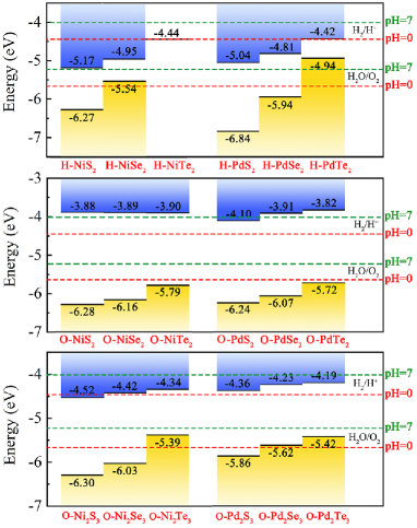
Here, in Fig. 6, by adopting HSE06 method, the accurate band alignments of monolayer TMCs are obtained. For the H-MX2 phase, the CBM and VBM never meet the requirement of redox potentials at pH=0 or 7, indicating that they can not be used for achieving water splitting. For the O-MX2 phase, the CBM and VBM are always higher and lower than the reduction and oxidation potentials at pH=0, respectively, implying that they have inherent advantage in realizing water splitting. When the pH of aqueous solution increases to 7, only the CBM of monolayer O-PdS2 fails in producing H2. For the O-M2X3 phase, both O-Ni2Se3 and O-Pd2S3 meet the redox potentials at pH=0, but they fail in realizing water splitting at pH=7. To further analysis the ability of water splitting, the kinetic overpotentials and (the difference between band edge and redox potential) are tested, which can represent properly the efficiency of driving the redox reaction (see details in Table S2 of the Supplementary Information). It shows that when pH of aqueous solution increases, decreases and increases. The pH value-dependent kinetic overpotential shows tunable ability of H2 production. These results imply that O-MX2, O-Ni2Se3 and O-Pd2S3 are possible photocatalysts for water splitting at specific pH of aqueous solution .
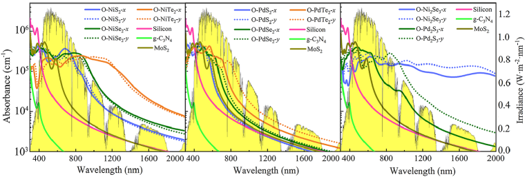
To investigate the actual performance, we need further consider the sunlight harvest of these candidates by calculating optical absorption coefficients. Using the GW approximation in conjunction with the Bethe-Salpeter equation (BSE) Rohlfing and Louie (2000); Deslippe et al. (2012), the light absorbance is obtained and plotted in Fig. 7. Here we include the electron-hole interaction in the optical calculation, as the charge screening effect is much weaker in two-dimension comparing to three-dimension due to the absence of screening along the out-of-plane direction. The solar energy is distributed in the infrared, visible and ultraviolet light about 43%, 50% and 7%, respectively. Fig. 7 shows that O-MX2, O-Ni2Se3 and O-Pd2S3 have ultrahigh absorption coefficients within both visible (400-760 nm) and ultraviolet ranges (760 nm), indicating their excellent harvest of the solar energy. As a comparison, we perform optical calculations of widely used intrinsic silicon, and other 2D semiconductor photocatalysts, including g-C3N4 and MoS2. When the wavelength is longer than 400 nm, the absorption coefficients of our TMCs candidates are much higher than all other compared materials, for example, about ten times higher than the value of intrinsic silicon. specially, O-Ni2Se3 shows high and constantly absorption over the entire energy range of the sunlight. Our results identify that O-MX2, O-Ni2Se3 and O-Pd2S3 have large absorption coefficients from visible to ultraviolet light and provide congenital advantages for applications as photocatalyst. Furthermore, monolayer O-MX2, O-Ni2Se3 and O-Pd2S3 present highly anisotropic optical properties, consistent with their mechanical properties. These materials can be used also for polarization-dependent photodetectors, similar as these proposed for other 2D materials such as black phosphorus Guo et al. (2016).
IV CONCLUSIONS
In conclusion, we have studied three phases of monolayer transition metal chalcogenides H-MX2, O-MX2 and O-M2X3 (M= Ni, Pd; X= S, Se, Te). We systematically examined their structural, mechanical and electronic characteristics via first-principle calculations. All these structures are stable at room temperature, verified by time-dependent ab initio molecular dynamics simulations and their phonon dispersion. The calculated mechanical properties also show that H-MX2 is isotropic, while O-MX2 and O-M2X3 present highly in-plane anisotropy due to their reduced lattice symmetry. Furthermore, O-MX2 shows great auxeticity with giant negative in-plane Poisson’s ratios, which are comparable to other known two-dimensional materials. Hence, O-MX2 has ultra-low Young’s modulus. By calculating the band alignments and light absorption coefficients, we concluded that O-MX2, O-Ni2Se3 and O-Pd2S3 can be used as flexible water splitting photocatalysts within visible and ultraviolet light regions, because of their suitable band gaps, band edges and ultrahigh sunlight absorption.
ACKNOWLEDGEMENTS
This work is supported by the National Key RD Program of China (Grant No. 2018FYA0305800). Numerical calculations presented in this paper have been performed on a supercomputing system in the Supercomputing Center of Wuhan University.
References
- Radisavljevic et al. (2011) B. Radisavljevic, A. Radenovic, J. Brivio, V. Giacometti, and A. Kis, Nat. Nanotechnol. 6, 147 (2011).
- Wang et al. (2012) Q. H. Wang, K. Kalantar-Zadeh, A. Kis, J. N. Coleman, and M. S. Strano, Nat. Nanotechnol. 7, 699 (2012).
- Lopez-Sanchez et al. (2013) O. Lopez-Sanchez, D. Lembke, M. Kayci, A. Radenovic, and A. Kis, Nat. Nanotechnol. 8, 497 (2013).
- Koppens et al. (2014) F. H. L. Koppens, T. Mueller, P. Avouris, A. C. Ferrari, M. S. Vitiello, and M. Polini, Nat. Nanotechnol. 9, 780 (2014).
- Mak et al. (2012) K. F. Mak, K. He, J. Shan, and T. F. Heinz, Nat. Nanotechnol. 7, 494 (2012).
- Zeng et al. (2012) H. Zeng, J. Dai, W. Yao, D. Xiao, and X. Cui, Nat. Nanotechnol. 7, 490 (2012).
- Li et al. (2014) L. Li, Y. Yu, G. J. Ye, Q. Ge, X. Ou, H. Wu, D. Feng, X. H. Chen, and Y. Zhang, Nat. Nanotechnol. 9, 372 (2014).
- Qiao et al. (2014) J. Qiao, X. Kong, Z.-X. Hu, F. Yang, and W. Ji, Nat. Commun. 5, 4475 (2014).
- Gomes and Carvalho (2015) L. C. Gomes and A. Carvalho, Phys. Rev. B 92, 085406 (2015).
- Hanakata et al. (2016) P. Z. Hanakata, A. Carvalho, D. K. Campbell, and H. S. Park, Phys. Rev. B 94, 035304 (2016).
- Xu et al. (2017) L. Xu, M. Yang, S. J. Wang, and Y. P. Feng, Phys. Rev. B 95, 235434 (2017).
- Tian et al. (2016) H. Tian, J. Tice, R. Fei, V. Tran, X. Yan, L. Yang, and H. Wang, Nano Today 11, 763 (2016).
- Kou et al. (2015) L. Kou, C. Chen, and S. C. Smith, J. Phys. Chem. Lett. 6, 2794 (2015).
- Wang et al. (2015) X. Wang, A. M. Jones, K. L. Seyler, V. Tran, Y. Jia, H. Zhao, H. Wang, L. Yang, X. Xu, and F. Xia, Nat. Nanotechnol. 10, 517 (2015).
- Li et al. (2018) E. Li, D. Wang, P. Fan, R. Zhang, Y.-Y. Zhang, G. Li, J. Mao, Y. Wang, X. Lin, S. Du, and H.-J. Gao, Nano Res. 11, 5858 (2018).
- Chow et al. (2017) W. L. Chow, P. Yu, F. Liu, J. Hong, X. Wang, Q. Zeng, C.-H. Hsu, C. Zhu, J. Zhou, X. Wang, J. Xia, J. Yan, Y. Chen, D. Wu, T. Yu, Z. Shen, H. Lin, C. Jin, B. K. Tay, and Z. Liu, Adv. Mater. 29, 1602969 (2017).
- Zeng et al. (2019) L.-H. Zeng, D. Wu, S.-H. Lin, C. Xie, H.-Y. Yuan, W. Lu, S. P. Lau, Y. Chai, L.-B. Luo, Z.-J. Li, and Y. H. Tsang, Adv. Funct. Mater. 29, 1806878 (2019).
- Oyedele et al. (2017) A. D. Oyedele, S. Yang, L. Liang, A. A. Puretzky, K. Wang, J. Zhang, P. Yu, P. R. Pudasaini, A. W. Ghosh, Z. Liu, C. M. Rouleau, B. G. Sumpter, M. F. Chisholm, W. Zhou, P. D. Rack, D. B. Geohegan, and K. Xiao, J. Am. Chem. Soc. 139, 14090 (2017).
- Nguyen et al. (2018) G. D. Nguyen, L. Liang, Q. Zou, M. Fu, A. D. Oyedele, B. G. Sumpter, Z. Liu, Z. Gai, K. Xiao, and A.-P. Li, Phys. Rev. Lett. 121, 086101 (2018).
- Lin et al. (2017) J. Lin, S. Zuluaga, P. Yu, Z. Liu, S. T. Pantelides, and K. Suenaga, Phys. Rev. Lett. 119, 016101 (2017).
- Iwase et al. (2011) A. Iwase, Y. H. Ng, Y. Ishiguro, A. Kudo, and R. Amal, J. Am. Chem. Soc. 133, 11054 (2011).
- Maeda and Domen (2010) K. Maeda and K. Domen, J. Phys. Chem. Lett. 1, 2655 (2010).
- Wang et al. (2008) P. Wang, B. Huang, X. Qin, X. Zhang, Y. Dai, J. Wei, and M.-H. Whangbo, Angew. Chem., Int. Ed. 47, 7931 (2008).
- Fujishima and Honda (1972) A. Fujishima and K. Honda, Nature 238, 37 (1972).
- Lu et al. (2016) Q. Lu, Y. Yu, Q. Ma, B. Chen, and H. Zhang, Adv. Mater. 28, 1917 (2016).
- Zhang et al. (2012) Y. Zhang, J. Liu, G. Wu, and W. Chen, Nanoscale 4, 5300 (2012).
- Kresse and Furthmüller (1996) G. Kresse and J. Furthmüller, Phys. Rev. B 54, 11169 (1996).
- Blöchl (1994) P. E. Blöchl, Phys. Rev. B 50, 17953 (1994).
- Perdew et al. (1996) J. P. Perdew, K. Burke, and M. Ernzerhof, Phys. Rev. Lett. 77, 3865 (1996).
- Monkhorst and Pack (1976) H. J. Monkhorst and J. D. Pack, Phys. Rev. B 13, 5188 (1976).
- Grimme (2006) S. Grimme, J. Comp. Chem. 27, 1787 (2006).
- Kerber et al. (2008) T. Kerber, M. Sierka, and J. Sauer, J. Comp. Chem. 29, 2088 (2008).
- Heyd et al. (2005) J. Heyd, J. E. Peralta, G. E. Scuseria, and R. L. Martin, J. Chem. Phys. 123, 174101 (2005).
- Gonze et al. (1994) X. Gonze, J.-C. Charlier, D. Allan, and M. Teter, Phys. Rev. B 50, 13035 (1994).
- Gonze and Lee (1997) X. Gonze and C. Lee, Phys. Rev. B 55, 10355 (1997).
- Giannozzi et al. (1991) P. Giannozzi, S. de Gironcoli, P. Pavone, and S. Baroni, Phys. Rev. B 43, 7231 (1991).
- Gale and Rohl (2003) J. D. Gale and A. L. Rohl, Mol. Simulat. 29, 291 (2003).
- Gale (1997) J. D. Gale, J. Chem. Soc., Faraday Trans. 93, 629 (1997).
- Zhou et al. (2018) J. Zhou, J. Lin, X. Huang, Y. Zhou, Y. Chen, J. Xia, H. Wang, Y. Xie, H. Yu, J. Lei, D. Wu, F. Liu, Q. Fu, Q. Zeng, C.-H. Hsu, C. Yang, L. Lu, T. Yu, Z. Shen, H. Lin, B. I. Yakobson, Q. Liu, K. Suenaga, G. Liu, and Z. Liu, Nature 556, 355 (2018).
- Shao et al. (2017) Y. Shao, S. Song, X. Wu, J. Qi, H. Lu, C. Liu, S. Zhu, Z. Liu, J. Wang, D. Shi, S. Du, Y. Wang, and H.-J. Gao, Appl. Phys. Lett. 111, 113107 (2017).
- Miró et al. (2014) P. Miró, M. Ghorbani-Asl, and T. Heine, Angew. Chem., Int. Ed. 53, 3015 (2014).
- Zhong et al. (2018) H. Zhong, K. Huang, G. Yu, and S. Yuan, Phys. Rev. B 98, 054104 (2018).
- Wang and Geng (2017) V. Wang and W. T. Geng, J. Phys. Chem. C 121, 10224 (2017).
- Lee et al. (2008) C. Lee, X. Wei, J. W. Kysar, and J. Hone, Science 321, 385 (2008).
- Çakır et al. (2014) D. Çakır, F. M. Peeters, and C. Sevik, Appl. Phys. Lett. 104, 203110 (2014).
- Gao et al. (2017) Z. Gao, X. Dong, N. Li, and J. Ren, Nano Lett. 17, 772 (2017).
- Zhang et al. (2015) S. Zhang, J. Zhou, Q. Wang, X. Chen, Y. Kawazoe, and P. Jena, Proc. Natl. Acad. Sci. 112, 2372 (2015).
- Wang et al. (2016) Y. Wang, F. Li, Y. Li, and Z. Chen, Nat. Commun. 7, 11488 (2016).
- Xiao et al. (2018) W.-Z. Xiao, G. Xiao, Q.-Y. Rong, and L.-L. Wang, Phys. Chem. Chem. Phys. 20, 22027 (2018).
- Zhang et al. (2016) L.-C. Zhang, G. Qin, W.-Z. Fang, H.-J. Cui, Q.-R. Zheng, Q.-B. Yan, and G. Su, Sci. Rep. 6, 19830 (2016).
- Kang et al. (2013) J. Kang, S. Tongay, J. Zhou, J. Li, and J. Wu, Appl. Phys. Lett. 102, 012111 (2013).
- Bolts and Wrighton (1976) J. M. Bolts and M. S. Wrighton, J. Phys. Chem. 80, 2641 (1976).
- Li et al. (2015) X. Li, J. Yu, J. Low, Y. Fang, J. Xiao, and X. Chen, J. Mater. Chem. A 3, 2485 (2015).
- Pham et al. (2014) T. A. Pham, D. Lee, E. Schwegler, and G. Galli, J. Am. Chem. Soc. 136, 17071 (2014).
- Committee (2008) G. Committee, ASTM International , DOI: 10.1520/G0173 (2008).
- Rohlfing and Louie (2000) M. Rohlfing and S. G. Louie, Phys. Rev. B 62, 4927 (2000), 50.
- Deslippe et al. (2012) J. Deslippe, G. Samsonidze, D. A. Strubbe, M. Jain, M. L. Cohen, and S. G. Louie, Comput. Phys. Commun. 183, 1269 (2012).
- Guo et al. (2016) Q. Guo, A. Pospischil, M. Bhuiyan, H. Jiang, H. Tian, D. Farmer, B. Deng, C. Li, S.-J. Han, H. Wang, Q. Xia, T.-P. Ma, T. Mueller, and F. Xia, Nano Lett. 16, 4648 (2016).