Modified transverse Ising model for the dielectric properties of SrTiO3 films and interfaces
Abstract
The transverse Ising model (TIM), with pseudospins representing the lattice polarization, is often used as a simple description of ferroelectric materials. However, we demonstrate that the TIM, as it is usually formulated, provides an incorrect description of SrTiO3 films and interfaces because of its inadequate treatment of spatial inhomogeneity. We correct this deficiency by adding a pseudospin anisotropy to the model. We demonstrate the physical need for this term by comparison of the TIM to a typical Landau-Ginzburg-Devonshire model. We then demonstrate the physical consequences of the modification for two model systems: a ferroelectric thin film, and a metallic LaAlO3/SrTiO3 interface. We show that, in both cases, the modified TIM has a substantially different polarization profile than the conventional TIM. In particular, at low temperatures the formation of quantized states at LaAlO3/SrTiO3 interfaces only occurs in the modified TIM.
Keywords: strontium titanate, interface, two-dimensional electron gas, transverse Ising model, ferroelectric films
1 Introduction
The transverse Ising model (TIM) was developed by deGennes in 1963 to describe the ferroelectric transition in hydrogen-bonded materials like potassium dihydrogen phosphate (KDP) [1]. As suggested by its name, the model formally describes a system of magnetic Ising moments in a transverse magnetic field [2], and since its discovery it has become significant because it is one of the simplest models to exhibit a quantum phase transition [3]. The focus of this work is more practical; we explore the use of the TIM to describe the dielectric properties of SrTiO3. Indeed, the TIM has been used widely to model the low-energy physics of systems in which local degrees of freedom can be represented by pseudospins [2]. In KDP, for example, the Ising spin states represent the two degenerate positions available to each hydrogen atom, while the transverse field represents the quantum mechanical tunneling between the states.
Because the TIM starts from a picture of fluctuating local dipole moments, it naturally describes materials, like KDP, with order-disorder transitions. However, the model has also been applied to materials like SrTiO3, which are close to a displacive ferroelectric transition. While there are some clear discrepancies between the model and experiments [4], the mean-field TIM nonetheless gives a useful quantitative phenomenology for the dielectric properties of both pure [5, 6] and doped[7, 8, 9, 10, 11] SrTiO3.
The local nature of the Ising pseudospins makes the TIM valuable as a model for inhomogeneous systems, including doped quantum paraelectrics [7, 8, 9, 10, 11], ferroelectric thin films [12, 13, 14, 15, 16, 17], superlattices [18, 19], and various low-dimensional structures [20, 21, 22]. However, we show here that the TIM, as it is conventionally formulated, fails to correctly describe SrTiO3 whenever nanoscale inhomogeneity is important. Most egregiously, the TIM fails to predict the formation of a quantized two-dimensional electron gas (2DEG) at LaAlO3/SrTiO3 interfaces, in contradiction with both theory and experiments [23]. The goal of this paper is to propose a modification that we believe captures the essential physics of spatial inhomogeneity, and to compare it to the conventional TIM for model SrTiO3 thin films and interfaces.
In the TIM, the lattice polarization in unit cell is modelled by a pseudospin. This polarization is given by
| (1) |
where sets the scale of the electric dipole moment, is the volume density of dipoles, and is the lattice constant. The pseudospin is usually taken to be , and is the third component of the corresponding three-dimensional pseudospin vector . The other two components, and , are fictitious degrees of freedom, with only the projection of onto the -axis corresponding to the physical polarization. (The unpolarized state is therefore described by the pseudospin lying entirely in the - plane.) In a quantum model, is the expectation value of the operator , which is identical to the spin matrix but which acts within pseudospin space.
The simplest version of the TIM is [6]
| (2) |
where plays the role of a transverse magnetic field that flips the Ising spins, is a nearest-neighbour coupling constant with indicating nearest-neighbour sites, and is the electric field in unit cell . For , the model tends towards a ferroelectric state at low temperatures; however, this is limited by , which disorders the ferroelectric state. Under mean-field theory the model predicts a ferroelectric phase transition only if , where is the coordination number of the lattice.
Although the TIM is only microscopically justified for order-disorder ferroelectrics, it is often used as a tool to characterize ferroelectrics of all types, and variations of this model have been applied to ferroelectricity in perovskites, including BaTiO3 [24] and SrTiO3 (STO) [6]. As a phenomenological model, the TIM is more complex than simple Landau-Ginzburg-Devonshire theories; however, it is also more versatile. The TIM, for example, is particularly well-suited to doped quantum paraelectrics, namely Sr1-xMxTiO3 with M typically representing Ca or Ba [7, 8, 9, 10, 25, 11]. In these materials, small dopant concentrations are sufficient to induce a ferroelectric transition. Several groups have successfully modeled these materials as binary alloys of SrTiO3 and MTiO3 with doping-independent model parameters [8, 9, 10, 25, 11].
The current work is motivated by the application of the TIM to metallic LaAlO3/SrTiO3 (LAO/STO) interfaces. These, and other related perovskite interfaces, have been widely studied since the discovery in 2004 that a 2DEG appears spontaneously at the interface when the LAO film is more than four unit cells thick [26]. This system is rich with interesting properties, including coexisting ferromagnetism and superconductivity [27, 28, 29], nontrivial spin-orbit effects [30, 31], a metal-insulator transition [32, 33], gate-controlled superconductivity [34], and a possible nematic transition at (111) interfaces [35, 36, 37, 38]. Furthermore, STO’s proximity to the ferroelectric state has led to suggestions that quantum fluctuations shape its band structure [39] and support superconductivity [40, 41]. More generally, there has been a growing appreciation that lattice degrees of freedom play a key role in shaping the electronic structure near LAO/STO interfaces [42, 43, 44, 45]. With this in mind, the recent discovery that ferroelectric-like properties persist in some metallic perovskites [46] naturally leads one to explore the effects of Ca or Ba doping on LAO/STO interfaces and, as described above, the TIM provides a natural framework in which to do this.
We found, however, that the TIM as it is usually formulated in equation (2) cannot reproduce the interfacial 2DEG and therefore fails to describe even the simple LAO/STO interface. In this work, we explain the reason for this failure and propose a modification to the TIM. In section 2, we introduce the modified model and by comparison with the standard Landau-Ginzburg-Devonshire (LGD) expansion, illustrate why the failure arises and how we fix it. As a simple example, we apply the modified model to ferroelectric thin films. In section 3, we then apply the model to the LAO/STO interface, and show explicitly how the modification allows for the formation of the 2DEG.
2 Inhomogeneous Ferroelectrics
We begin by describing a modified TIM (section 2.1) that contains an additional anisotropic interaction; depending on its sign, this interaction generates either a pseudospin easy axis or easy plane. We obtain mean-field equations for the pseudospin and susceptibility, and by comparison to the LGD theory (section 2.2) we show that the Landau parameters are under-determined by the conventional TIM. Essentially, the problem is that equation (2) contains three adjustable parameters (, , and ), while the simplest LGD model requires four parameters to describe an inhomogeneous system. The additional interaction in the modified TIM fixes this discrepancy. In sections 2.3 and 2.4 we obtain fits to the model parameters for the case of STO. As a simple application, in section 2.5 we explore how the new term modifies the polarization distribution of a ferroelectric thin film.
2.1 The Modified TIM
The modified Hamiltonian for general pseudospin is
| (3) |
This is equivalent to the Blume-Capel model in a transverse magnetic field [47]. The third term introduces an anisotropic pseudospin energy. If , this term tends to align dipoles along the (3)-axis, making it an easy axis, which enhances the polarization; if , the term tilts the dipole away from the (3)-axis, creating an easy plane and reducing the polarization.
The TIM is traditionally formulated with a spin- pseudospin. In that case, is written in terms of a Pauli spin matrix, and is proportional to the identity operator. The new term therefore does not produce the desired anisotropy when . This problem does not exist for higher spin models, and for this reason we formulate the TIM in terms of a general pseudospin . However, we will show below that at the mean-field level, the model provides nearly the same results for any value of , and for simplicity we revert to when we show results as a way of gaining insight into the general case.
Applying mean-field theory to equation (3) gives the following self-consistent expression for :
| (4) |
where
| (5) |
is the Brillouin function, , is temperature, , and is the -component of the Weiss mean field for lattice site ,
| (6) |
The summation is a sum over the nearest neighbours of site , and therefore depends on whether pseudospin is in a surface or bulk layer.
We linearize equation (4) to obtain the condition that ensures ferroelectricity. In the uniform case,
| (7) |
where
| (8) |
for coordination number . At zero-temperature, , and from equation (4) the model therefore predicts a paraelectric-ferroelectric phase transition when
| (9) |
From this one sees that, for any , a ferroelectric transition occurs at nonzero temperature only when . In the case of a paraelectric like STO, .
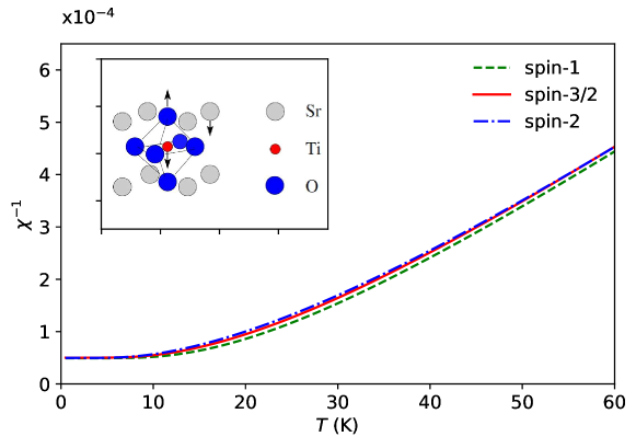
To show that the choice of has a small effect at the mean-field level, the uniform inverse dielectric susceptibility of STO is plotted for different values of in figure 1. From equation (1), the susceptibility for a weak uniform electric field is
| (10) |
where is obtained from equation (4) with given by equation (7). Figure 1 shows results for , and . The fitting parameters , , and depend on the value of and were determined by fitting to the experimental susceptibility, as described in section 2.3 below. (Note that is not explicitly used here because the calculations are for bulk STO.) The values of all these parameters are listed in table 1.
Because the model was fitted to low- and high-temperature susceptibilities, the curves in figure 1 are expected to be close in value at these limits. However, they also differ only slightly in between, indicating that STO is well-described by the simplest case shown, , when using mean-field theory. In particular, the model accurately captures both Curie-Weiss behaviour at high temperature, and the saturation of the susceptibility at low temperature (where the ferroelectric transition is suppressed by quantum fluctuations).
2.2 Comparison to the Landau-Ginzburg-Devonshire Expansion
While equation (4) is the fundamental self-consistent equation for , the role each parameter plays in determining the pseudospin is not transparent. For example, it is not immediately evident from this expression why the conventional TIM (with ) is unable to describe inhomogeneous systems. To explore this point, we expand equation (4) in powers of and compare the coefficients to those in a typical LGD expansion. We show that the transition temperature and correlation length cannot be set independently unless is nonzero.
The typical LGD free energy with order parameter has the form
| (11) | |||||
is the electric field, , , and are the LGD coefficients that describe the material, and is the inverse volume of a unit cell. Minimizing equation (11) with respect to gives the familiar equation
| (12) |
which can be solved for the pseudospin. The critical temperature is set by , which changes sign at the ferroelectric transition, while determines the zero-temperature polarization. In the paraelectric phase, is determined by the dielectric susceptibility and and set the correlation length .
We expand equation (4) in powers of to obtain
| (13) |
where and are defined by equation (6). To proceed further, we note that the discretized second derivative of a function is
| (14) |
Then, equation (6) can be re-written as
| (15) |
with defined by equation (8). This can now be substituted into equation (13).
Keeping only terms that are directly comparable to those in equation (12), we obtain
| (16a) | |||||
| (16b) | |||||
| (16c) | |||||
| (16d) | |||||
These equations show that and are determined by combinations of and , while and are determined by and , respectively. The key point is that reduces to for the conventional TIM, in which case and are not independent. Physically, this means that the correlation length, which sets the length scale over which the material responds to inhomogeneities, cannot be determined independently of the transition temperature and low- polarization. In other words, the four coefficients , , and are only described by three parameters, , and .
In this case, the model predicts a significantly smaller correlation length at low temperatures than does the modified TIM. From equations (16a) and (16c),
| (16q) |
At low temperatures, . In this case, the conventional TIM () gives Å, independent of . For , the range of correlation lengths from the modified TIM, where the values are taken from table 1, is 2.9-6.1 nm, which is an order of magnitude larger. The pseudospin anisotropy is therefore an essential part of the TIM.
2.3 Fitting , , and for SrTiO3
Most of the TIM parameters can be fit to existing susceptibility data. We do this for STO, as it will form the basis of our discussion in section 3.
Inserting equation (4) into equation (10), we obtain the susceptibility
| (16r) |
where , is given by equation (7), and
| (16s) |
At high temperatures, this expression simplifies. Taking , equation (16r) obtains a Curie-Weiss form,
| (16t) |
where K [48] is the transition temperature implied by the high-temperature susceptibility. (In STO, this transition is suppressed by quantum fluctuations.) and are thus obtained by matching equation (16t) to high- experiments.
At low , equation (16r) takes one of two forms depending on whether the system is ferroelectric or not. For a ferroelectric, can be found from the behaviour of the susceptibility at for critical temperature . In this case, , , and setting the denominator of equation (16r) to zero gives a self-consistent equation for ,
| (16u) |
For a paraelectric like STO, on the other hand, we obtain from the zero-temperature susceptibility. In this limit and equation (16r) may easily be inverted for . The values of , and for STO determined from equation (16r) are listed in table 1.
The closeness in value between and for STO can be understood from their physical meanings. sets the temperature at which a transition would occur in the absence of quantum fluctuations, while sets the scale of the quantum fluctuations; that these two are close in value is because STO is close to a ferroelectric transition. Further, since the Curie-Weiss temperature is small, both of these parameters are small.
2.4 Estimating for SrTiO3
As was shown in section 2.2, sets the scale of the gradient term in the LGD expansion, and it can therefore be obtained from quantities related to spatial gradients of the polarization. In perovskites, the polarization is closely connected to an optical phonon mode [49, 39], pictured in figure 1. One can therefore obtain from the phonon dispersion.
Key to this analysis is that the optical phonon has a large dipole moment that is represented by the TIM pseudospins. The phonon spectrum can therefore be obtained from the dynamical pseudospin correlation function. In the paraelectric phase, the term proportional to in equation (3) ensures that the pseudospins lie primarily along the (1)-axis. Perturbations of this state can be viewed as the magnons of a fictitious ferromagnetic material in which the magnetic moments align along the (1)-axis. The phonons can then be described as spin-wave excitations.
The spin operators are difficult to work with, however, and it is useful to bosonize them. This is achieved with the Holstein-Primakoff transformation [50, 51]. This transformation maps the pseudospin operators on to the boson creation and annihilation operators, and . Pseudospin projections on the (3)-axis are then modelled as boson excitations, with a pseudospin that is entirely polarized along the (1)-axis represented by the vacuum state.
In this representation, the raising and lowering operators for site differ from the typical set by a cyclic permutation of the pseudospin axes. We then define [50]
| (16va) | |||||
| (16vb) | |||||
| (16vwa) | |||||
| (16vwb) | |||||
Since the polarization lies close to the (1)-axis in the paraelectric state, only low bosonic excitation states are relevant. In this case, and . Additionally, the (1)-component of the pseudospin is defined as [50]
| (16vwx) |
and the (3)-component is
| (16vwy) | |||||
| (16vwz) |
Because represents atomic displacements, and are therefore phonon operators.
Equations (16vwx) and (16vwy) can now be substituted into equation (3). We transform to reciprocal space using = :
| (16vwaa) |
where , is the total number of lattice sites, and
| (16vwaba) | |||||
| (16vwabb) | |||||
Note that we have set here, since the phonon spectrum is measured at zero field.
It is convenient to formulate the dynamics of the pseudomagnons using Green’s functions. The Green’s functions are correlation functions between the pseudomagnon creation and annihilation operators, and the equations of motion of the Green’s functions therefore include the equations of motion of and . The spin-wave excitation spectrum can then be obtained from the poles of the Green’s function.
The Green’s function and its equation of motion are, respectively,
| (16vwabac) |
| (16vwabad) |
where is the step function. The second Green’s function that appears in equation (16vwabad) and its equation of motion are
| (16vwabae) |
| (16vwabaf) |
Fourier transforming equations (16vwabad) and (16vwabaf) in time and solving for gives the following expression for the Green’s function:
| (16vwabag) |
The phonon dispersion is therefore given by
| (16vwabaha) | |||||
| (16vwabahb) | |||||
We obtain an expression for by comparing the frequency at and the zone centre:
| (16vwabahai) |
where the subscripts and 0 indicate and , respectively. Since is already known from bulk susceptibility data, can be estimated solely using the material’s phonon dispersion. Using neutron scattering data from [49], we obtained a range of values between 30 and 200 meV depending on and on how the fit was made. As will be shown in section 3, these estimates are somewhat lower than the values required to produce a 2DEG at the LAO/STO interface, which is likely a limitation of the TIM. Nonetheless, this calculation shows that is orders of magnitude larger than the value that is implicit in the conventional TIM.
This large discrepancy between and is a key feature of STO, and that there is more than an order of magnitude difference between their values can be related to their different physical origins. Further, from equation (8) it follows that is not small; rather, it is negative and nearly cancels . would however play less of a role in a material with a high transition temperature, where and would be closer in value.
2.5 Ferroelectric Thin Films
We first model the polarization in ferroelectric thin films as a simple application of the modified TIM. A ferroelectric’s properties can vary drastically between the bulk and thin-film forms, and the origins and applications of these differences have been increasingly studied in recent years [52]. Ferroelectric thin films provide significant advantages in electronic devices such as increased efficiency in photovoltaic cells [53, 54, 55] and decreased power usage in non-volatile memory storage [56].
We focus on weakly ferroelectric materials, like those obtained by doping STO with 18O, Ca, or Ba. We take , and we thus fix the parameters meV and Å, which were determined in section 2.3 for STO. To obtain a ferroelectric transition, we take meV, which yields a bulk transition temperature K, similar to what is observed in Sr1-xCaxTiO3. We treat as an adjustable parameter.
Thin films have a layered geometry that simplifies calculations. Taking each layer to be one unit cell thick, and assuming translational invariance within the -plane, the pseudospin, electric field, and polarization depend only on the layer index (instead of site ). Equation (4) becomes
| (16vwabahaj) |
where and the Weiss mean field is
| (16vwabahak) |
where, for the cubic STO crystal structure, the sum over nearest neighbours of a pseudospin in layer is . The lattice polarization in layer is then
| (16vwabahal) |
(Recall that is the maximum dipole moment per unit cell and is the dipole moment density.)
We assume a short-circuit geometry, in which the top and bottom surfaces of the film are connected by a wire that maintains a zero voltage difference between them. This geometry is commonly adopted to minimize the effects of depolarizing electric fields. We thus have two kinds of charge: a bound charge coming from a sum of atomic and lattice polarizations, and the external charges on the top and bottom electrodes.
The electric field in equation (16vwabahak) is obtained from these charges via Gauss’ law,
| (16vwabaham) |
We break the polarization into lattice and atomic pieces, and respectively, with the atomic polarizability, and defining the optical dielectric constant [57, 58], we obtain the usual expression
| (16vwabahan) |
which can be integrated to find .
The charge density in the top and bottom electrodes is written as
| (16vwabahao) |
where is the film thickness, and is the positive charge per 2D unit cell on the top electrode. Integrating equation (16vwabahan) gives
| (16vwabahap) |
A second integration, of equation (16vwabahap) across the thickness of the film, gives
| (16vwabahaq) |
with the potential difference across the film. Using this to eliminate in equation (16vwabahap), and setting for the short-circuit geometry, we obtain
| (16vwabahar) |
with the average polarization of the film. Equations (16vwabahak) and (16vwabahar) are evaluated at discrete positions , and together with equation (16vwabahaj) form a closed set that can be solved self-consistently.
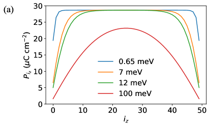
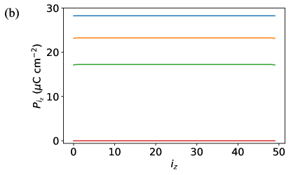
Figure 2 shows the results of simulations for a film that is layers thick. The figure illustrates two main points: First, the results depend qualitatively on whether or not electric fields are included in the simulation, even in the short-circuit geometry (for which naive considerations suggest the field vanishes); second, for fixed , the value of has a large impact on the polarization.
The effects of electric fields in thin films were discussed at length by Kretschmer and Binder [59], and the results in figure 2 serve as a reminder of their importance. In figure 2(a), where electric fields are not included, the polarization is reduced at the surfaces and increases to its bulk value over a length scale set by the correlation length. In the ferroelectric phase, the correlation length is (in terms of LGD parameters), which is proportional to . The conventional TIM with has meV, which corresponds to a correlation length of Å. Consistent with this, figure 2(a) shows that for the conventional TIM, surface effects are confined to narrow regions near the edges of the film. Conversely, the modified TIM with a more realistic value of meV gives the correlation length nm, which is comparable to the film thickness. In this case, the polarization is inhomogeneous throughout the film. In contrast to both of these cases, the polarization is nearly constant across the film when electric fields are included [figure 2(b)]; the polarization decreases with increasing , and is suppressed completely for meV.
The apparent uniformity of the polarization across the film in figure 2(b) is because the correlation length is replaced by a shorter length scale when electric fields are included, with [59]
| (16vwabahas) |
In STO, this length scale is less than a unit cell, and the polarization is therefore nearly constant, with only a small reduction in the surface layer. This slight reduction is, nonetheless, enough that the depolarizing fields are incompletely screened by the electrodes. There is thus a residual depolarizing field in the STO film that reduces the overall polarization of the film.
To make the dependence of on the TIM parameters explicit, we substitute values for the LGD parameters from equations (16a)-(16d) into equation (16vwabahas) in the limit . For spin-1 we find
| (16vwabahat) |
For fixed and (i.e. for a fixed value of the bulk ), increases as . Because the difference between the polarizations at the film surface and interior depends on , the depolarizing field also grows with ; it then follows immediately that decreases as increases. This suppression is illustrated in figure 3(a), which shows the dependence of both the average polarization and on . The polarization equals its bulk value when and drops as increases. Notably, there is a critical value of (which depends on the number of layers, , in the film) above which ferroelectricity is completely suppressed. For the 50-layer film modelled here, this value is approximately 17 meV.
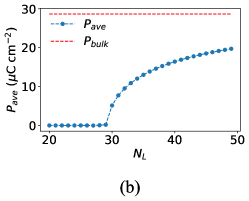
Alternatively, one can fix and consider how depends on film thickness, as shown in figure 3(b). Here polarization increases and asymptotically approaches the bulk value with increasing . Ferroelectricity is completely suppressed below a critical film thickness, with the value of this critical thickness depending on . The results shown in figure 3(b) are for meV, and give a critical thickness of 30 layers. For meV, the critical thickness is closer to 300 layers.
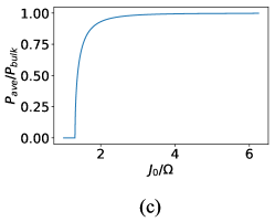
Finally, the effect of increasing is shown in figure 3(c). Because the bulk value of polarization depends on , we show the ratio as a function of . In bulk materials, the threshold for ferroelectricity is , and this is increased by finite size effects in the 50-layer film as shown in figure 3(c). Size effects quickly become unimportant with increasing , as rapidly increases towards its bulk value. Indeed, when is only twice , .
These calculations show that doped quantum paraelectrics such as Sr1-xCaxTiO3, which have close to , should be highly sensitive to film thickness in the short-circuit geometry. While this might be naively anticipated based on the argument that the correlation length is comparable to the film thickness near a ferroelectric transition, this argument is wrong because the relevant length is actually rather short and does not diverge at the quantum critical point. Rather, the sensitivity is due to depolarizing fields, which can easily overwhelm the weak ferroelectricity.
3 (001) LAO/STO Interface
In the final section of this work, we apply the modified TIM to the (001) LAO/STO interface. For this calculation, the Hamiltonian must include an electronic term that describes the 2DEG that forms at the interface. The total Hamiltonian is thus
| (16vwabahau) |
where is given by equation (3) and is the electronic term discussed below. These two terms are linked through the electric field, which appears explicitly in , and appears implicitly in through the electrostatic potential.
We outline the calculations in section 3.1, and show results for the effect of on the interfacial 2DEG in section 3.2. The main result from this section is that the conventional and modified TIM make very different predictions for the structure of the 2DEG.
3.1 Method
We assume that the 2DEG arises due to a combination of top gating and the polar catastrophe. In this case a total charge density is donated from the LAO surface to the interface, where is the surface hole density, in order to neutralize the polar discontinuity between the two materials. Top gating gives control over the number of free electrons doped into the system.
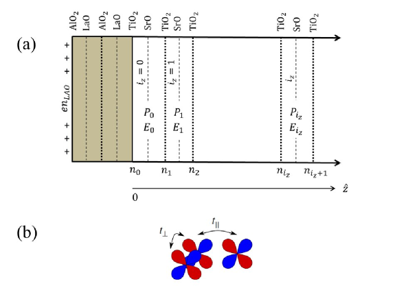
As shown in figure 4(a), we adopt a discretized model comprising alternating metallic TiO2 layers with electron densities and dielectric layers with polarizations . Translational invariance is assumed within the -plane, but not along the -axis perpendicular to the interface. The system’s properties are therefore only dependent on layer.
The 2DEG is composed of electrons that occupy titanium orbitals in the STO substrate. Although the unit cell is tetragonally distorted both by unit cell rotations about the -axis and by interfacial strains, to a good approximation we can assume STO has the cubic structure typical of a perovskite material, as shown in the inset of figure 1. We adopt a tight-binding model in which the conduction bands are made up of orbitals [57, 60, 61], and assume that electrons only hop between orbitals of the same type (ie. from one orbital to another orbital; other hopping matrix elements vanish in the cubic phase by symmetry, and are generally small when lattice distortions are included).
3.1.1 Electronic Hamiltonian
The electronic Hamiltonian is made up of a hopping kinetic energy and an electrostatic potential energy :
| (16vwabahav) |
The hopping energy is
| (16vwabahaw) |
where creates an electron with spin and orbital type in the 2D plane-wave state in layer . is a sum over nearest-neighbour layers and . is the hopping matrix element for an electron in orbital type hopping along path to a nearest-neighbour site. is the atomic energy of an orbital site in layer , and can be set to zero in calculations.
In the tight-binding model, there are six possible hopping paths. Hopping along corresponds to a displacement and hopping amplitude , and so on for hopping along and . Then, equation (16vwabahaw) simplifies to
| (16vwabahax) |
where . As illustrated in figure 4(b), the amplitudes and are denoted by for hopping paths that lie in the plane defined by , and for hopping paths that are perpendicular to this plane. We take eV and eV as in [57].
The electrostatic potential energy is due to the charge on the LAO surface, the 2DEG, and the bound charge due to the polarization of the STO:
| (16vwabahay) |
where is electron charge and is the electrostatic potential in layer .
Combining equations (16vwabahax) and (16vwabahay) gives the full electronic Hamiltonian:
| (16vwabahaz) | |||||
The Hamiltonian can be written as an matrix in the layer index, , with and
| (16vwabahba) |
where is independent of and is the identity matrix. The eigenergies are particularly simple, with
| (16vwabahbb) |
where are the eigenvalues of and is the band index. The eigenvectors of , which represent the layer-dependent wavefunctions, are -independent and satisfy
| (16vwabahbc) |
From this, the free electron density (per unit cell) in layer is
| (16vwabahbd) |
where is the total number of - and -points, and is the Fermi-Dirac distribution.
We note that the mean-field equations described in this section neglect thermal fluctuations of both the lattice and the charge density. Both of these broaden the electronic spectral functions, as in Fermi liquid theory, and can in principle mix the bands. These are perturbative effects, however, and band structure calculations like the one outlined here generally provide a good quantitative description of the electronic structure, even at room temperature.
3.1.2 Electric Field
The electric potential in layer is obtained by integrating the electric field from layer 0 to layer , which sets the interface to be the zero of potential. Then,
| (16vwabahbe) |
with Å the STO lattice constant.
Just as in section 2.5, the electric field can be obtained using Gauss’ law,
| (16vwabahbf) |
where is the free charge density and is the external charge density along the LAO surface. The polarization is obtained from the modified TIM.
Within the discretized model, the electrons are treated as if they are confined to two-dimensional TiO2 layers, so
| (16vwabahbg) |
where is given by equation (16vwabahbd). Similarly, the external charge density is confined to the top LAO layer,
| (16vwabahbh) |
where is the distance from the interface to the LAO surface. Now, integrating equation (16vwabahbf) over gives the electric field in layer :
| (16vwabahbi) |
which is required for the TIM [equation (3)] and the electric potential [equation (16vwabahbe)].
3.2 Results
Here, we explore the effect that has on the electron distribution, eigenenergies, polarization and potential energy for the (001) LAO/STO interface. As a key point of comparison, these calculations include the case meV (), which corresponds to the conventional TIM, in order to clearly highlight why the modified TIM requires the term introduced in equation (3) to correctly model interfaces.
Previous work has established that the 2DEG is composed of both interfacial and tail components. The interfacial component is tightly confined to the interface, and appears as a peak in the electron density extending over the first few layers of the substrate, while the tail component extends far into the STO substrate [62, 63, 64, 23, 45]. Except at the very lowest dopings, the majority of the electrons are confined close to the interface, with as many as 70% of the electrons in the 2DEG found in approximately the first 10 nm [57, 62]. This interfacial peak in the electron density is strongly temperature- and electron doping-dependent, with the electrons spreading further out into the STO as temperature or doping decreases [57]. The first band contributes the most electrons to the interface states, while the first and bands make up the majority of the tail states and are seen to have the most temperature-dependence [57].
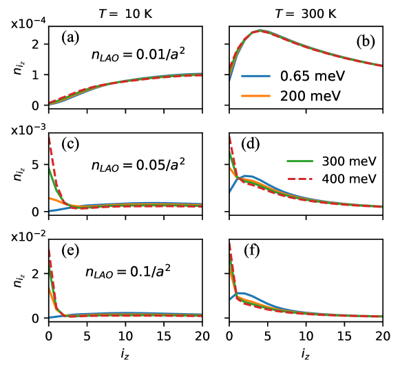
The electron density is plotted in figures 5 and 6. Figure 5 explores the effect has on the electron density, focusing particularly on the interface region, while figure 6 shows the full profile over the entire film for a typical set of model parameters.
We begin analyzing figure 5 by focusing on the results of the conventional TIM. When meV, there is no evidence that electrons are confined to the interface region at 10 K at any doping, in disagreement with experiments. Weak confinement does appear at 300 K due to the reduced dielectric susceptibility at high , and the 2DEG does move towards the interface with increasing doping; however, the density is expected to be strongly peaked at the interface, and this is not seen. The conventional TIM, therefore, does not capture the physics of STO interfaces.
The remaining curves in figure 5 show how the charge profile changes with increasing . These results are for fixed and (which determine the uniform dielectric susceptibility), and the only difference between the curves is therefore the correlation length . These curves show that increasing (or equivalently, increasing ) tends to increase electron density at the interface, except at the lowest doping.
At the lowest doping, , has little effect on the electron density at both high and low temperature. Indeed, interface states are absent for all values up to 400 meV. While this lack of interface states is consistent with previous calculations [45], it is not consistent with experiments [65, 66], and likely points to some additional missing physics in the model [45].
At intermediate doping, , the electron density does develop an interfacial component as increases. This interfacial state extends only a few unit cells from the interface, and is more tightly confined at large . There is thus a clear qualitative distinction between the modified and conventional TIMs in this case. At high doping, , the trends are similar. The electron density is confined closer to the interface and is less strongly temperature dependent than at lower doping, at least when meV. Both of these trends are consistent with results reported in [57].
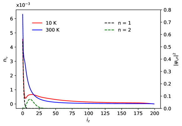
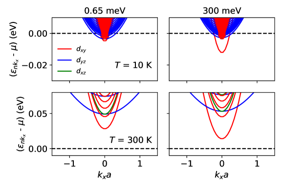
Figure 6 shows the electron density across the full thickness of the STO film for a typical value at intermediate doping for both 10 K and 300 K. We choose the value of meV as physically reasonable based on the results in figure 5. At 10 K, the charge profile shows a peak-dip-hump structure that has not been reported in previous calculations. To understand its origin, we plot also the wavefunctions for the first () and second () bands () at 10 K. These show that the dip comes from the extremely tight confinement of the first band to the interface.
The band structure is shown in figure 7 for intermediate doping for both the conventional TIM and the modified TIM ( meV). At 10 K, the band structures of the two models are quasi-continuous, which is indicative of deconfined tail states, except for a single band that sits below the continuum in the modified TIM, and which corresponds to the interface state discussed above. At high , the band structures are discrete, which is indicative of confinement to the interface region. At this temperature, the effects of are quantitative, rather than qualitative.
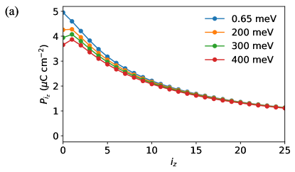
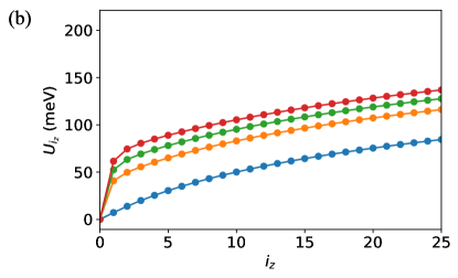
Finally, we plot in figure 8 the polarization and potential energy at 300 K for intermediate doping. These plots show that there are clear distinctions between the conventional and modified TIMs in the interfacial region. In particular, the polarization near the interface is reduced, by up to 25%, as increases. This reduction is similar to that discussed in the case of the thin film, with one key difference: because electric fields are screened by the 2DEG, the relevant length scale over which differences between the curves decay in figure 8(a) is , and not [39].
Similar to the ferroelectric thin films discussed in section 2.5, this reduced polarization incompletely screens the electric fields produced by the LAO surface charge and results in a large field at the interface. This is reflected in the potential energy profiles shown in figure 8(b). In particular, large values of generate a deep potential well that confines the lowest band tightly to the interface. On the other hand, has little effect on the electric field away from the interface, and so each potential energy curve has roughly the same slope for . In summary, figure 8 illustrates the mechanism by which the anisotropic pseudospin term in the modified TIM generates the interfacial component of the 2DEG that is observed at LAO/STO interfaces.
4 Conclusions
We showed that the conventional transverse Ising model misses key features of spatially inhomogeneous STO-based nanostructures. To fix this we modified the TIM by adding an anisotropic pseudospin energy to the Hamiltonian. This corrects a deficiency of the TIM, namely that if one fits the model parameters to the bulk (homogeneous) susceptibility, the polarization correlation length is also fixed by the model and is at least an order of magnitude smaller than it should be.
To illustrate the effects of the new term, we considered two applications of the modified TIM: first, to thin films of an STO-like ferroelectric; and second, to a metallic LAO/STO interface. In both cases, the key point is that the conventional TIM underestimates the reduction of the polarization due to the surface; this reduced polarization leads to a reduced screening of electric fields in the interface region, which in turn has profound effects on the film or interface. In the case of the ferroelectric film, these fields depolarize the polarization in the film; in the case of the interface, they create a confining potential that generates tightly bound interface states.
References
References
- [1] de Gennes P G 1963 Solid State Commun. 1 132–137
- [2] Stinchcombe R B 1973 J. Phys. C Solid State 6 2459–2483
- [3] Sachdev S 2011 Quantum Phase Transitions (Cambridge: Cambridge University Press) ISBN 9780521514682
- [4] Muller K A and Burkard H 1979 Phys. Rev. B 19 3593–3602
- [5] Hemberger J, Lunkenheimer P, Viana R, Böhmer R and Loidl A 1995 Phys. Rev. B 52 13159–13162
- [6] Hemberger J, Nicklas M, Viana R, Lunkenheimer P, Loidl A and Böhmer R 1996 J. Phys.: Condens. Matter 8 4673–4690
- [7] Kleemann W, Dec J, Wang Y G, Lehnen P and Prosandeev S A 2000 J. Physics Chem. Solids 61 167–176
- [8] Zhang L, Kleemann W and Zhong W L 2002 Phys. Rev. B 66 104105
- [9] Wang Y G, Kleemann W, Dec J and Zhong W L 1998 Europhys. Lett. 42 173–178
- [10] Wu H and Jiang Q 2003 J. Phys.: Condens. Matter 15 2849–2858
- [11] Guo Y J, Guo Y Y, Lin L, Gao Y J, Jin B B, Kang L and Liu J M 2012 Phys. Rev. B 86 014202
- [12] Wang C L, Zhong W L and Zhang P L 1992 J. Phys.: Condens. Matter 4 4743–4749
- [13] Sun P N, Lü T Q, Chen H and Cao W W 2008 Chin. Phys. Lett. 25 3422–3425
- [14] Oubelkacem A, Essaoudi I, Ainane A, Saber M, Gonzalez J and Bärner K 2009 Physica B 404 4190–4197
- [15] Wang C D, Teng B H, Ju Y F, Cheng D M and Zhang C L 2010 Commun. Theor. Phys. 54 756–762
- [16] Lu Z X 2013 Eur. Phys. J. App. Phys. 63 30301
- [17] Li Z P 2016 Phase Transitions 89 1119–1128
- [18] Wang C L, Xin Y, Wang X S, Zhong W L and Zhang P L 2000 Phys. Lett. A 268 117–122
- [19] Wu Y Z, Yao D L and Li Z Y 2002 Phys. Stat. Sol. B 231 561–571
- [20] Xin Y, Wang C L, Zhong W and Zhang P 1999 Phys. Lett. A 260 411–416
- [21] Lang X Y and Jiang Q 2007 J. Nanopart. Res. 9 595–603
- [22] Lu Z X 2014 Eur. Phys. J. App. Phys. 66 10403
- [23] Gariglio S, Fête A and Triscone J M 2015 J. Phys.: Condens. Matter 27 283201
- [24] Zhang L, Zhong W L and Kleemann W 2000 Phys. Lett. A 276 162–166
- [25] Tao Y M and Jiang Q 2004 Chin. Phys. 13 1149–1155
- [26] Ohtomo A and Hwang H Y 2004 Nature 427 423–426
- [27] Brinkman A, Huijben M, van Zalk M, Huijben J, Zeitler U, Maan J C, van der Wiel W G, Rijnders G, Blank D H A and Hilgenkamp H 2007 Nature Mat. 6 493–496
- [28] Reyren N et al 2007 Science 317 1196–1199
- [29] Dikin D A, Mehta M, Bark C W, Folkman C M, Eom C B and Chandrasekhar V 2011 Phys. Rev. Lett. 107 056802
- [30] Shalom M B, Sachs M, Rakhmilevitch D, Palevski A and Dagan Y 2010 Phys. Rev. Lett. 104 126802
- [31] Caviglia A D, Gabay M, Gariglio S, Reyren N, Cancellieri C and Triscone J M 2010 Phys. Rev. Lett. 104 126803
- [32] Thiel S, Hammerl G, Schmehl A, Schneider C W and Mannhart J 2006 Science 313 1942–1945
- [33] Liao Y C, Kopp T, Richter C, Rosch A and Mannhart J 2011 Phys. Rev. B 83 075402
- [34] Caviglia A D, Gariglio S, Reyren N, Jaccard D, Schneider T, Gabay M, Thiel S, Hammerl G, Mannhart J and Triscone J M 2008 Nature 456 624–627
- [35] Miao L, Du R, Yin Y and Li Q 2016 App. Phys. Lett. 109 261604
- [36] Davis S, Chandrasekhar V, Huang Z, Han K, Ariando and Venkatesan T 2017 Phys. Rev. B 95 035127
- [37] Boudjada N, Wachtel G and Paramekanti A 2018 Phys. Rev. Lett. 120 086802
- [38] Boudjada N, Khait I and Paramekanti A 2019 Phys. Rev. B 99 195453
- [39] Atkinson W A, Lafleur P and Raslan A 2017 Phys. Rev. B 95 054107
- [40] Edge J M, Kedem Y, Aschauer U, Spaldin N A and Balatsky A V 2015 Phys. Rev. Lett. 115 247002
- [41] Dunnett K, Narayan A, Spaldin N A and Balatsky A V 2018 Phys. Rev. B 97 144506
- [42] Behtash M, Nazir S, Wang Y and Yang K 2016 Phys. Chem. Chem. Phys. 18 6831–6838
- [43] Lee P W, Singh V N, Guo G Y, Liu H J, Lin J C, Chu Y H, Chen C H and Chu M W 2016 Nat. Commun. 7 12773
- [44] Gazquez J, Stengel M, Mishra R, Scigaj M, Varela M, Roldan M A, Fontcuberta J, Sánchez F and Herranz G 2017 Phys. Rev. Lett. 119 106102
- [45] Raslan A and Atkinson W A 2018 Phys. Rev. B 98 195447
- [46] Rischau C W et al 2017 Nature Phys. 13 643–648
- [47] Albayrak E 2013 Chinese Physics B 22 077501
- [48] Sakudo T and Unoki H 1971 Phys. Rev. Lett. 26 851–853
- [49] Cowley R A 1964 Phys. Rev. 134 A981
- [50] Mohn P 2003 Magnetism in the Solid State: An Introduction vol 134 (Heidelberg: Springer) ISBN 3540431837
- [51] Holstein T and Primakoff H 1940 Phys. Rev. 58 1098–1113
- [52] Setter N et al 2006 J. Appl. Phys. 100 051606
- [53] Liu Y, Wang S F, Chen Z J and Xiao L X 2016 Sci. China Mater. 59 851–866
- [54] Zenkevich A, Matveyev Y, Maksimova K, Gaynutdinov R, Tolstikhina A and Fridkin V 2014 Phys. Rev. B 90 161409
- [55] Kutes Y, Ye L, Zhou Y, Pang S, Huey B D and Padture N P 2014 J. Phys. Chem. Lett. 5 3335–3339
- [56] Müller J, Böscke T S, Bräuhaus D, Schröder U, Böttger U, Sundqvist J, Kücher P, Mikolajick T and Frey L 2011 Appl. Phys. Lett. 99 112901
- [57] Raslan A, Lafleur P and Atkinson W A 2017 Phys. Rev. B 95 054106
- [58] Zollner S, Demkov A A, Liu R, Fejes P L, Gregory R B, Alluri P, Curless J A, Yu Z, Ramdani J, Droopad R, Tiwald T E, Hilfiker J N and Woollam J A 2000 Journal of Vacuum Science & Technology B: Microelectronics and Nanometer Structures Processing, Measurement, and Phenomena 18 2242
- [59] Kretschmer R and Binder K 1979 Phys. Rev. B 20 1065–1076
- [60] Stengel M 2011 Phys. Rev. Lett. 106 136803
- [61] Khalsa G and MacDonald A H 2012 Phys. Rev. B 86 125121
- [62] Copie O et al 2009 Phys. Rev. Lett. 102 216804
- [63] Dubroka A et al 2010 Phys. Rev. Lett. 104 156807
- [64] Park S Y and Millis A J 2013 Phys. Rev. B 87 205145
- [65] Yin C, Seiler P, Tang L M K, Leermakers I, Lebedev N, Zeitler U and Aarts J ArXiv:1904.03731, 2019
- [66] Joshua A, Pecker S, Ruhman J, Altman E and Ilani S 2012 Nat. Commun. 3 1129