Accurate metasurface synthesis incorporating near-field coupling effects
Abstract
One of the most promising metasurface architectures for the microwave and terahertz frequency ranges consists of three patterned metallic layers separated by dielectrics. Such metasurfaces are well suited to planar fabrication techniques and their synthesis is facilitated by modelling them as impedance sheets separated by transmission lines. We show that this model can be significantly inaccurate in some cases, due to near-field coupling between metallic layers. This problem is particularly severe for higher frequency designs, where fabrication tolerances prevent the patterns from being highly-subwavelength in size. Since the near-field coupling is difficult to describe analytically, correcting for it in a design typically requires numerical optimization. We propose an extension of the widely used equivalent-circuit model to incorporate near-field coupling and show that the extended model can predict the scattering parameters of a metasurface accurately. Based on our extended model, we introduce an improved metasurface synthesis algorithm that gives physical insight to the problem and efficiently compensates for the perturbations induced by near-field coupling. Using the proposed algorithm, a Huygens metasurface for beam refraction is synthesized showing a performance close to the theoretical efficiency limit despite the presence of strong near-field coupling.
pacs:
I Introduction
Metasurfaces are thin sheets of subwavelength resonators which have emerged as a versatile platform for wavefront manipulation, addressing applications from microwave to visible frequencies Yu and Capasso (2014); Ding et al. (2018); Chen et al. (2018). Where high transmission efficiency is required, Huygens metasurfaces are widely used as they feature equal electric and magnetic dipole responses to suppress spurious reflections Pfeiffer and Grbic (2013a); Monticone et al. (2013); Decker et al. (2015). Different metasurface architectures and corresponding synthesis methods have been proposed within the last two decades Ding et al. (2018). For microwave to terahertz frequencies, most reported work is based on planar stacks of three patterned metallic layers, separated by dielectric substrates, as this architecture is compatible with planar circuit manufacturing techniques Chen et al. (2018); Epstein and Eleftheriades (2016a); Pfeiffer and Grbic (2014). In addition to Huygens metasurfaces, the same approach has been used to realize bianisotropic metasurfaces, which are more efficient for very large refraction angles Wong et al. (2016); Cole et al. (2018); Fathnan and Powell (2018).
In synthesizing metasurfaces, it is often necessary to assume that meta-atoms are small compared to the wavelength. This has motivated the development of deeply subwavelength meta-atoms Wong et al. (2014); Epstein and Eleftheriades (2016a), with feature sizes on the order of . For metasurfaces operating at W-band frequencies (75 - 110 GHz) and higher, the resulting feature sizes are too small for conventional printed circuit board fabrication techniques, so simpler geometries such as dogbone Lavigne et al. (2018); Capolino et al. (2013); Rabinovich and Epstein (2018) must be used. This frequency range is of interest for applications such as wireless communication Rappaport et al. and radar Patole et al. ; Hasch et al. , and metasurfaces should enable devices such as efficient transmitarray antennas Pfeiffer and Grbic (2013b); Jiang et al. . Despite the high potential for applications, to the best of our knowledge, there is only one work reporting transmissive refracting metasurfaces operating at W-band frequencies Pfeiffer and Grbic (2013b). Efficient modelling of near-field interaction would enable metasurfaces to be synthesized with simpler geometries, which are feasible to fabricate for this frequency range.
In modelling multilayered printed circuit metasurfaces, each metallic layer is represented by an equivalent surface impedance and the dielectric layers in between are treated as transmission line sections (See Fig. 1) Epstein and Eleftheriades (2016b); Pfeiffer and Grbic (2013b); Monticone et al. (2013). The advantage of this model is that it yields expressions for the required surface impedance of each metallic layer, greatly simplifying the process of designing the metasurface. The transmission line model accounts for the propagation of the fundamental Floquet harmonic within a periodic metasurface, neglecting all higher-order harmonics, since they are evanescent. Neglecting evanescent waves is accurate for structures with large separation relative to the wavelength, however in metasurfaces it is usually required that the separation between the metallic layers is small. Thus near-field coupling between the layers is neglected. As we show here, this approximation is significantly inaccurate in cases of practical interest, and can lead to performance degradation. Therefore, accurate modelling and synthesis of transmissive metasurfaces must take account of near-field effects between metallic layers. We note that the near-field coupling effects that are investigated here are not related to the evanescent waves (or auxiliary fields) deliberately introduced in Ref. Epstein and Eleftheriades, .
Early works on near-field interaction in metamaterials aimed to model the propagation of magneto-inductive waves in arrays of split ring resonators Syms et al. (2005), to analyze tunability through modifying lattice parameters Powell et al. (2010) and to analyze optical activity of twisted dimers Liu et al. (2007, 2012). Furthermore, several recent works propose analytical design approaches for metagratings based on rigorous descriptions of the mutual interaction of individual particles Chalabi et al. (2017); Ra’di et al. (2017); Rabinovich and Epstein (2018); Popov et al. (2018); Epstein and Rabinovich (2018). While these works on near-field coupling in metagratings provide full insight into the interaction of individual scatterers and demonstrate highly efficient devices, they have been largely restricted to reflective operation at large angles. More recently, near-field effects within and between cells of a metasurface have been investigated in gap plasmon structures Deshpande et al. (2018); Sharac et al. . For other important metasurface geometries, especially those for operation in transmission, near-field coupling is still largely unexplored and achieving the designed transmission response often requires black-box optimization Lavigne et al. (2018); Cole et al. (2018) or ad hoc iterative design methods Pfeiffer and Grbic (2013b).
In this paper, we demonstrate how the model of cascaded impedance sheets can be significantly inaccurate due to near-field coupling between metallic layers. We propose an extension of this model to incorporate near-field coupling and show that the extended model can predict the scattering parameters of metasurfaces accurately. This proposed coupling model does not require the explicit calculation of electromagnetic interaction integrals as in previous works Powell et al. (2010); Liu et al. (2012). The inaccuracies caused by near-field coupling can hamper the synthesis of transmissive multilayer metasurfaces. Therefore, we introduce an improved synthesis algorithm based on the proposed model, which provides good physical insight and reduced computational effort compared to black-box optimization. The algorithm is applied to a homogeneous Huygens metasurface with dogbone resonators, then to an inhomogeneous metasurface exhibiting anomalous refraction.
II Design of metasurfaces with three metallic layers
The model of cascaded impedance sheets is widely used in the literature for the analysis of transmissive metasurfaces Monticone et al. (2013); Epstein and Eleftheriades (2016b); Pfeiffer and Grbic (2013b). With this model, the properties of each layer are specified based on the scattering properties of the multi-layer stack, allowing the synthesis to be reduced to readily solvable problems. However, the model does not account for near-field coupling between layers, which can lead to significant inaccuracy. In the following, we briefly recapitulate the model and show that neglecting near-field coupling can lead to significant inaccuracy in the design of a homogeneous Huygens metasurface.
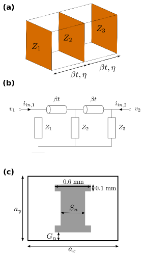
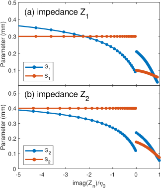
Each metallic layer is represented by a shunt impedance and the dielectric layers are represented by a transmission line with propagation constant , wave impedance and thickness Tretyakov (2003) as depicted in Figure 1(a). Utilizing a circuit analogy, currents are equivalent to the magnetic field and voltages are equivalent to the electric field Tretyakov (2003). The transimssion line model accounts for far-field (or first order Floquet) coupling between the metallic-layers. It is difficult to calculate a meaningful propagation angle within a single meta-atom, therefore within each cell propagation normal to the surface is assumed Epstein and Eleftheriades (2016b). The corresponding circuit for the three layer system is shown in Figure 1(b). Using this circuit, the network parameters of each cell can be determined by cascading the individual building blocks in terms of transmission (ABCD) matrices , where the transmission matrix of a shunt impedance and a transmission line are defined in Appendix A. The transmission matrix of the complete cell is transformed into a scattering matrix . In Ref. Epstein and Eleftheriades (2016b) it was shown how the designed transmission response of the cell leads to specification for each of the three sheet impedances shown in Fig. 1. We perform numerical simulations of the dogbone structure to create a lookup table relating its geometric parameters to the sheet impedance , which is shown in Fig. 2. We note that the relationship between impedance and geometric parameters differs between the inner and outer layers due to the difference in surrounding dielectric medium.
To apply the model, we synthesize one unit cell of a Huygens metasurface for operation in the millimeter wave band at 80 GHz with the metallic layers having the dogbone geometry depicted in Figure 1(c). With the smallest metallic feature size of 0.1 mm, a substrate thickness of m and a permittivity of =3.0, this unit cell design is compatible with standard printed circuit board fabrication while operating at W-band frequencies (similar to Ref. Pfeiffer and Grbic, 2013b). This results in relatively large resonators, with lateral unit cell dimensions of . To allow comparison with theory, we assume lossless dielectric layers, and perfectly conducting metal patterns with zero thickness. Since Huygens metasurfaces are symmetrical, the first and third layer are identical, i.e. , and .
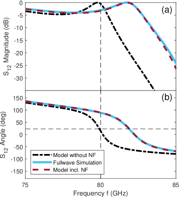
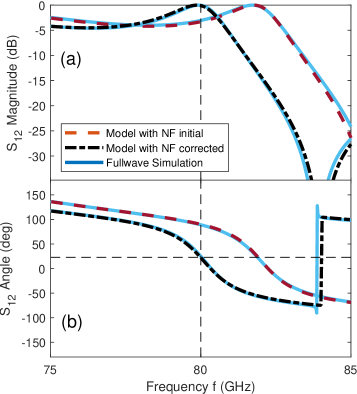
The metasurface is designed to reach near unity transmission amplitude and a transmission phase response of at frequency . In Figure 3, the transmission response of the model (black dashed line) is compared to results from full wave simulation (blue solid line). The model predicts that transmission is close to unity amplitude and meets the expected phase at . However, full wave simulation reveals that the transmission maximum and the corresponding phase are significantly shifted to 81.9 GHz. We attribute this discrepancy to near-field coupling (or equivalently higher order Floquet modes), which is to be expected, given that . This clearly demonstrates that this widely-used model can fail for some geometries of practical interest, and consequently it is not precise enough for the synthesis of metasurfaces having high efficiency.
III Modelling near-field coupling between layers
Here we extend the model of metasurfaces with three metallic layers to incorporate near-field coupling between the layers. We note that the presented model is quite general and could also be applied to bianisotropic metasurfaces, or to designs containing four or more layers Abdo-Sanchez et al. (2018); Liu et al. (2016); Pan et al. (2018); Jiang et al. (2018).
III.1 Near-field impedance matrix
We extend the circuit model shown in Figure 1(b) by accounting for the mutual impedance between each of the metallic layers. As shown in Fig. 4, this is represented within the equivalent circuit model by current controlled voltage sources. To facilitate our analysis, we include a virtual port at the location of the centre metallic layer. Consistent with the existing model, we assume that propagation within a single meta-atom is normal to the surface.

We introduce the near-field impedance matrix which gives the near-field relationship between the equivalent voltages and currents on each of the metallic layers
| (1) |
The diagonal terms are the self impedances of layer and the off diagonal elements are the transfer impedances of the corresponding current controlled voltage sources, hence they represent coefficients that quantify the near-field coupling between layer and . We consider only reciprocal structures, therefore is a symmetric matrix with . Also note that the use of a scalar current to represent the current flow on a metallic layer is valid so long as only one mode can be excited on it.
To relate to the scattering parameters of the entire cell, we first convert it to admittance parameters . The admittance matrix of the complete cell relates the equivalent current flowing into to each port to the equivalent voltages
| (2) |
Admittance matrix represents the far-field contribution of the transmission lines through their equivalent current .
| (3) |
where we introduce the total transmission line current at the central node as . An analytical expression for is given in Appendix A.
Using the relation and Eq. (1) to (3), we can write
| (4) |
Using these admittance matrices, near-field and far field contributions to the inter-layer coupling simply sum up and can be linked to the network parameters of the complete cell system .
As no current can flow through the virtual port 2 of Fig. 4, we impose the condition . This leads to a reduced admittance matrix for the complete cell, defined as
| (5) |
with its relationship to shown in Appendix A.
Given a near-field impedance matrix , the reduced two port admittance matrix can be determined using equation Eqs. (4) and (11). This is then converted to a scattering matrix , to obtain transmission and reflection properties of the metasurface. Note that if the near-field coupling coefficients are set to zero, this formalism is equivalent to the existing model outlined in Section II.
III.2 Determination of the near-field impedance terms
To apply the formalism developed in Subsection III.1 to metasurface analysis, it is necessary to find the values of elements of . Since is a 3x3 matrix and is a 2x2 matrix, a single far-field scattering simulation yields insufficient information to resolve . Therefore, we propose a technique to determine the elements of successively from full wave simulations of reduced systems containing only two layers. A two layer formalism analogous to Section III.1 is applied to these full-wave scattering parameters, which allows the unambiguous extraction of individual elements of . This two layer formalism is outlined in Appendix A.
A typical configuration for a full wave simulation of the unit cell of a metasurface with three layers is shown in Fig. 5 (a). The unit cell is centered at , periodic boundary conditions apply to all sides and Floquet ports are located at a large distance to the top and bottom of the structure, where the influence of high order Floquet modes is negligible. The reference plane of these ports however needs to be moved back to the top and bottom to , respectively, to correct the reflection and transmission phase Epstein and Eleftheriades (2016a).
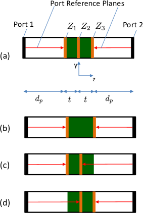
By removing the central metallic layer, as shown in Fig. 5(b), the two layer formalism can be applied to determine the self impedance of layers one and three, and , and their mutual impedance . To determine , and , the configuration from Fig. 5(c) is utilized. Here, however, the reference plane of Port 2 needs to be moved to the central metal layer, which can be done by inverting the ABCD matrix of the dielectric layer Pozar (2011). Similarly, , and can be obtained from the configuration from Fig. 5 (d). Using this successive approach, the full coupling matrix is determined and the three layer system is fully characterized.
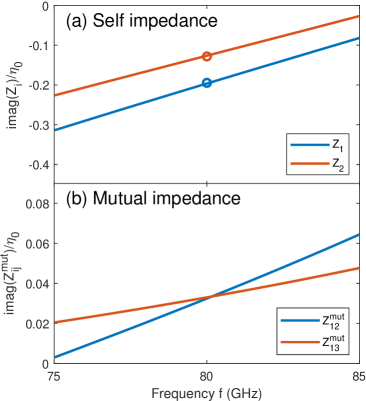
We apply this technique to the metasurface considered in Section II to determine the near-field impedance matrix . As we consider a Huygens metasurface with and , only two simulations are required to determine the near-field impedance matrix , since the configurations in Figure 5(c) and (d) are equivalent. The resulting self impedances and mutual impedances are shown in Figure 6. As we consider lossless structures, these functions are purely imaginary to within numerical accuracy (). At the design frequency, the mutual impedance and are clearly smaller than the self impedance and , however they are not negligible. The mutual and self impedance terms have the form of a series LC circuit. Using the calculated near-field impedance matrix, the metasurface transmission is plotted in Figure 3 (red dashed line), showing good agreement with the full wave simulation. This result confirms the accuracy of our near-field coupling model, demonstrating why the conventional metasurface synthesis procedure fails in this case.
IV Metasurface synthesis incorporating near-field coupling
IV.1 Refinement algorithm for metasurface synthesis
Having characterized how near-field coupling can render existing metasurface design techniques inaccurate, we present an approach to include it within the metasurface synthesis. Since the near-field coupling cannot be evaluated until a geometry of the metal layer has been specified, this necessarily involves the use of an iterative algorithm. The goal of the algorithm is to find the geometrical parameters of the unit cell that match the target scattering parameters. In the case of Huygens metasurfaces, it is sufficient to minimize the difference between the realized transmission and designed transmission
| (6) |
The realized transmission is calculated from our near-field coupling model with the matrix . A fundamental assumption of the algorithm is that for small changes of self impedances , the geometric change is small, and the mutual coupling does not change strongly. This allows us to correct only the diagonal elements of the coupling matrix with a factor at each iteration
| (7) |
where the iteration index is denoted with . The factor is chosen by minimizing the term numerically in each iteration.
Based on the corrected self impedances , the geometry of the unit cell is updated with new geometrical parameters and using the lookup table in Figure 2. If a further iteration is necessary, the mutual impedances are recalculated with full wave simulations of the new geometry. Note that Eq. (7) could be modified to adjust outer layer impedances separately from the inner layer ones, however this was found empirically to offer no improvement in convergence. The optimization process is outlined in full in Algorithm 1.
| Initialize: |
| Start geometry: |
| Calculate self impedances from model |
| without near-field coupling and set geometry |
| accordingly |
| Calculate near-field coupling terms: |
| Determine , and |
| with full wave simulations obtaining |
| Start iterative steps: |
| while() |
| Initialize coupling matrix according to Eq. (7) |
| Calculate correction factor by minimizing |
| to get new |
| Update geometry accordingly |
| if then |
| terminate |
| end |
| Recalculate actual , and |
| with current geometry and update |
| p=p+1 |
| end |
The algorithm terminates when the relative change of the self impedances from one iteration to the next is smaller than . This convergence parameter was chosen as 0.085 for the examples shown in this work. The absolute value of the resulting correction factor for the self impedances ranged between 0.038 and 0.25. The ability of this algorithm to correct the transmission response of a cell is shown in Fig. 7. The red dashed line shows the initial response according to the design procedure outlined in Section II. The black dash-dot curve shows the result of the model after the optimization, and the blue lines show the corresponding results of full-wave simulation. It can be seen that the strong perturbation of the operating frequency has been corrected, and the metasurface now achieves complete transmission and the designed phase value at the operating frequency.
IV.2 Application to metasurface demonstrating anomalous refraction
We demonstrate the further utility of our iterative algorithm by applying it to an inhomogeneous Huygens metasurface demonstrating anomalous refraction of a plane wave. The incident angle was chosen and the refraction angle , leading to a supercell width mm. Each cell is based on the dogbone geometry shown in Fig. 1(a). To minimize the influence of coupling to non-identical neighboring cells which is not described in our model, the lateral spacing was chosen as large as possible. With the supercell width used here, there are three propagating Floquet modes in transmission, and , and three in reflection and . To control these 6 degrees of freedom, a minimum of three cells per supercell is required, each having an engineered electric and magnetic response.
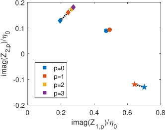
The initial sheet impedances and the required transmission response for each cell were specified according to the design procedure in Epstein and Eleftheriades (2016a). With these target values, impedance matching to the refracted wave is stipulated. The geometry of each cell was synthesized using the algorithm from Section IV.1. The self impedance of each cell at iteration is shown in Figure 8. In the case of the first cell, having identical geometry to that was analyzed in Section II, three iterations were necessary to obtain the required scattering properties. For the other two cells, one iteration was enough, due to the lesser influence of near-field coupling in these cases. The resulting geometrical parameters of the supercell are given in Table 1.
| Geometry Parameters [m] | ||||||||||||
|---|---|---|---|---|---|---|---|---|---|---|---|---|
| cell | 1 | 2 | 3 | |||||||||
| parameter | ||||||||||||
| before | 300 | 126 | 400 | 149 | 300 | 204 | 172 | 220 | 300 | 175 | 400 | 138 |
| after | 300 | 114 | 400 | 139 | 300 | 210 | 172 | 218 | 300 | 172 | 400 | 137 |
We note that an alternative approach to correct for near-field coupling is to use black-box optimization methods, which are built in to many commercial simulation packages. Compared to these methods, our proposed algorithm has several advantages. Unlike these black-box optimization methods, our approach gives clear physical insight into the near-field coupling which causes the metasurface design to be non-optimal. In particular, with the quantities , near-field coupling effects can be quantified and monitored from iteration to iteration. Additionally, our algorithm is much more computationally efficient, as is demonstrated by the results in Appendix B, which demonstrates a speed up factor of 3.6 for the design considered. For metasurface designs with a large number of cells, this speed up would also be a significant benefit. Furthermore, using the proposed algorithm, the influence of near-field coupling effects can be corrected without any prior knowledge. Applying black-box optimization methods requires guessing the required geometric parameter changes and setting suitable parameter boundaries.
While we considered only a single polarization in this work, we expect that our method could be adapted to tensorial impedances Selvanayagam and Eleftheriades (2016) used to model polarization rotating metasurfaces. We note that for chiral metasurfaces based on coupled high-symmetry layers Hannam et al. (2014), polarization rotation only occurs when near-field coupling is strong, thus near-field coupling cannot be neglected in equivalent circuit modelling.
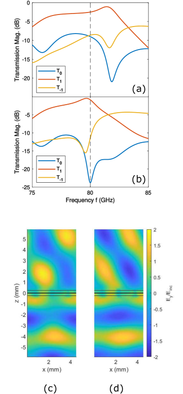
The refraction performance of the synthesized metasurface is shown in Figure 9, where , the transmission coefficient into the designed Floquet mode, should be maximized, and other terms minimized. The performance of the initial geometry (a) is compared with the performance of the geometry obtained by our iterative optimization process (b). For the initial metasurface, the energy refracted into the desired Floquet mode is as low as 56 % at the design frequency GHz. The maximum refraction efficiency is 78 %, but it is significantly shifted to 81.4 GHz. The optimized metasurface on the other hand refracts 82 % into the desired Floquet mode at the design frequency. In this case, the maximum refraction efficiency is 90 % at 79.7 GHz. We note that the maximum efficiency of the optimized metasurface is close to the theoretical efficiency limit Epstein and Eleftheriades (2016a) for Huygens metasurfaces, which is 92 % for a refraction angle of .
V Conclusion
We showed that metasurfaces based on patterned metallic layers separated by dielectric layers can exhibit strong inter-layer near-field coupling. This can lead to significant inaccuracy of existing models used for metasurface synthesis, resulting in poor performance of the metasurfaces. We developed an improved model which accounts for near-field coupling and showed that it closely matches the results of full-wave simulation. This is of particular significance for higher frequency designs, where fabrication tolerances mean that feature sizes are not highly sub-wavelength, leading to strong near-field coupling.
To mitigate the performance degradation induced by near-field coupling, we introduced an iterative algorithm for accurate metasurface synthesis which takes it into account. The presented algorithm gives more physical insight into the problem than black-box optimization, and reduces computation time significantly. Additionally, it is very generic and can be applied to multilayer metasurfaces in various frequency ranges. As this work introduces an efficient synthesis method for such geometries, it helps to relax fabrication requirements and pave avenues for new metasurface geometries.
Acknowledgements.
This work was financially supported by the Australian Research Council (Linkage Project LP160100253) and the Luxembourg Ministry of the Economy (grant CVN 18/17/RED).Appendix A Two and three-port matrix representations
The ABCD matrices of a shunt impedance and transmission line Pozar (2011) are given by
| (8) |
and
| (9) |
The admittance matrix for the three layer system can be determined analyzing the circuit from Figure 4 (b) without shunt elements and dependent sources utilizing the definition of an admittance matrix element and states
| (10) |
To reduce the three port equivalent circuit shown in Fig. 4 to a two-port network compatible with circuit simulations, we impose the condition . This yields the following expression for the two port matrix in terms of elements of the three port matrix
| (11) |
Equations (1) to (4) can be defined analogously for the two layer system using the 2x2 matrices , and . In the corresponding circuit model in Figure 10, the admittance matrix for the transmission line is
| (12) |
With known admittance matrix , we can determine without any ambiguity. The coefficients of for configuration (b) to (d) in Figure 5 are then used subsequently to build the 3x3 matrix . Note, that in configuration (b), the thickness is .

Appendix B Computational efficiency
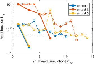
To evaluate the computation time of the algorithm proposed in this work, it was compared with a black-box trusted region framework algorithm implemented in the commercial package CST Microwave Studio Studio (2018). The merit function for the optimization is , as previously. By far the most significant contribution to the computation time comes from full wave simulations. Therefore, we compare here the number of full wave simulations that is required until the respective optimization algorithm converges for both of these methods. Since two full wave simulations are required to determine the near-field impedance matrix , the proposed model based optimization requires when terminating at iteration . The black-box optimization on the other hand requires .
In Figure 11, the computational effort for the two algorithms is compared in terms of , for each of the three cells in our anomalously refracting metasurface. Our proposed optimization technique was on average 3.6 times faster than the black-box optimization. Additionally, the trust region optimization requires some prior knowledge to set the boundaries of the parameter space. Here, we chose on the initial parameter set.
References
- Yu and Capasso (2014) Nanfang Yu and Federico Capasso, “Flat optics with designer metasurfaces,” Nature Materials 13, 139–150 (2014).
- Ding et al. (2018) Fei Ding, Anders Pors, and Sergey I Bozhevolnyi, “Gradient metasurfaces: A review of fundamentals and applications,” Reports on Progress in Physics 81, 026401 (2018).
- Chen et al. (2018) Michael Chen, Minseok Kim, Alex M.H. Wong, and George V. Eleftheriades, “Huygens’ metasurfaces from microwaves to optics: A review,” Nanophotonics 7 (2018), 10.1515/nanoph-2017-0117.
- Pfeiffer and Grbic (2013a) Carl Pfeiffer and Anthony Grbic, “Metamaterial Huygens’ Surfaces: Tailoring Wave Fronts with Reflectionless Sheets,” Physical Review Letters 110, 197401 (2013a).
- Monticone et al. (2013) Francesco Monticone, Nasim Mohammadi Estakhri, and Andrea Alù, “Full Control of Nanoscale Optical Transmission with a Composite Metascreen,” Physical Review Letters 110, 203903 (2013).
- Decker et al. (2015) Manuel Decker, Isabelle Staude, Matthias Falkner, Jason Dominguez, Dragomir N. Neshev, Igal Brener, Thomas Pertsch, and Yuri S. Kivshar, “High-Efficiency Dielectric Huygens’ Surfaces,” Advanced Optical Materials 3, 813–820 (2015).
- Epstein and Eleftheriades (2016a) Ariel Epstein and George V. Eleftheriades, “Huygens’ metasurfaces via the equivalence principle: Design and applications,” Journal of the Optical Society of America B 33, A31–A50 (2016a).
- Pfeiffer and Grbic (2014) Carl Pfeiffer and Anthony Grbic, “Bianisotropic Metasurfaces for Optimal Polarization Control: Analysis and Synthesis,” Physical Review Applied 2 (2014), 10.1103/PhysRevApplied.2.044011.
- Wong et al. (2016) Joseph P. S. Wong, Ariel Epstein, and George V. Eleftheriades, “Reflectionless Wide-Angle Refracting Metasurfaces,” IEEE Antennas and Wireless Propagation Letters 15, 1293–1296 (2016).
- Cole et al. (2018) Michael A. Cole, Aristeidis Lamprianidis, Ilya V. Shadrivov, and David A. Powell, “Refraction efficiency of Huygens’ and bianisotropic terahertz metasurfaces,” arXiv:1812.04725 [physics] (2018).
- Fathnan and Powell (2018) Ashif A. Fathnan and David A. Powell, “Bandwidth and size limits of achromatic printed-circuit metasurfaces,” Optics Express 26, 29440 (2018).
- Wong et al. (2014) Joseph P. S. Wong, Michael Selvanayagam, and George V. Eleftheriades, “Design of unit cells and demonstration of methods for synthesizing Huygens metasurfaces,” Photonics and Nanostructures - Fundamentals and Applications Metamaterials-2013 Congress, 12, 360–375 (2014).
- Lavigne et al. (2018) G. Lavigne, K. Achouri, V. S. Asadchy, S. A. Tretyakov, and C. Caloz, “Susceptibility Derivation and Experimental Demonstration of Refracting Metasurfaces Without Spurious Diffraction,” IEEE Transactions on Antennas and Propagation 66, 1321–1330 (2018).
- Capolino et al. (2013) Filippo Capolino, Andrea Vallecchi, and Matteo Albani, “Equivalent Transmission Line Model With a Lumped X-Circuit for a Metalayer Made of Pairs of Planar Conductors,” IEEE Transactions on Antennas and Propagation 61, 852–861 (2013).
- Rabinovich and Epstein (2018) Oshri Rabinovich and Ariel Epstein, “Analytical Design of Printed-Circuit-Board (PCB) Metagratings for Perfect Anomalous Reflection,” IEEE Transactions on Antennas and Propagation , 0018–926X, 1558–2221 (2018).
- (16) Theodore S. Rappaport, Yunchou Xing, George R. MacCartney, Andreas F. Molisch, Evangelos Mellios, and Jianhua Zhang, “Overview of Millimeter Wave Communications for Fifth-Generation (5G) Wireless Networks—With a Focus on Propagation Models,” 65, 6213–6230.
- (17) S. M. Patole, M. Torlak, D. Wang, and M. Ali, “Automotive radars: A review of signal processing techniques,” 34, 22–35.
- (18) J. Hasch, E. Topak, R. Schnabel, T. Zwick, R. Weigel, and C. Waldschmidt, “Millimeter-Wave Technology for Automotive Radar Sensors in the 77 GHz Frequency Band,” 60, 845–860.
- Pfeiffer and Grbic (2013b) C. Pfeiffer and A. Grbic, “Millimeter-Wave Transmitarrays for Wavefront and Polarization Control,” IEEE Transactions on Microwave Theory and Techniques 61, 4407–4417 (2013b).
- (20) Zhi Hao Jiang, Lei Kang, Wei Hong, and Douglas H. Werner, “Highly Efficient Broadband Multiplexed Millimeter-Wave Vortices from Metasurface-Enabled Transmit-Arrays of Subwavelength Thickness,” 9, 10.1103/PhysRevApplied.9.064009.
- Epstein and Eleftheriades (2016b) Ariel Epstein and George V. Eleftheriades, “Arbitrary Power-Conserving Field Transformations With Passive Lossless Omega-Type Bianisotropic Metasurfaces,” IEEE Transactions on Antennas and Propagation 64, 3880–3895 (2016b).
- (22) Ariel Epstein and George V. Eleftheriades, “Synthesis of Passive Lossless Metasurfaces Using Auxiliary Fields for Reflectionless Beam Splitting and Perfect Reflection,” 117, 10.1103/PhysRevLett.117.256103.
- Syms et al. (2005) R. R. A. Syms, Ekaterina Shamonina, V. Kalinin, and L. Solymar, “A theory of metamaterials based on periodically loaded transmission lines: Interaction between magnetoinductive and electromagnetic waves,” Journal of Applied Physics 97, 064909–064909 (2005).
- Powell et al. (2010) David A. Powell, Mikhail Lapine, Maxim V. Gorkunov, Ilya V. Shadrivov, and Yuri S. Kivshar, “Metamaterial tuning by manipulation of near-field interaction,” Physical Review B 82 (2010), 10.1103/PhysRevB.82.155128.
- Liu et al. (2007) H. Liu, D. Genov, D. Wu, Y. Liu, Z. Liu, C. Sun, S. Zhu, and X. Zhang, “Magnetic plasmon hybridization and optical activity at optical frequencies in metallic nanostructures,” Physical Review B 76, 073101–073101 (2007).
- Liu et al. (2012) Mingkai Liu, David A. Powell, Ilya V. Shadrivov, and Yuri S. Kivshar, “Optical activity and coupling in twisted dimer meta-atoms,” Applied Physics Letters 100, 111114 (2012).
- Chalabi et al. (2017) H. Chalabi, Y. Ra’di, D. L. Sounas, and A. Alù, “Efficient anomalous reflection through near-field interactions in metasurfaces,” Physical Review B 96 (2017), 10.1103/PhysRevB.96.075432.
- Ra’di et al. (2017) Younes Ra’di, Dimitrios L. Sounas, and Andrea Alù, “Metagratings: Beyond the Limits of Graded Metasurfaces for Wave Front Control,” Physical Review Letters 119 (2017), 10.1103/PhysRevLett.119.067404.
- Popov et al. (2018) Vladislav Popov, Fabrice Boust, and Shah Nawaz Burokur, “Controlling Diffraction Patterns with Metagratings,” Physical Review Applied 10 (2018), 10.1103/PhysRevApplied.10.011002.
- Epstein and Rabinovich (2018) Ariel Epstein and Oshri Rabinovich, “Perfect Anomalous Refraction with Metagratings,” arXiv:1804.02362 [physics] (2018).
- Deshpande et al. (2018) Rucha Deshpande, Vladimir A. Zenin, Fei Ding, N. Asger Mortensen, and Sergey I. Bozhevolnyi, “Direct Characterization of Near-Field Coupling in Gap Plasmon-Based Metasurfaces,” Nano Letters (2018), 10.1021/acs.nanolett.8b02393.
- (32) Nicholas Sharac, Alexander J. Giles, Keith Perkins, Joseph Tischler, Francisco Bezares, Sharka M. Prokes, Thomas G. Folland, Orest J. Glembocki, and Joshua D. Caldwell, “Implementation of plasmonic band structure to understand polariton hybridization within metamaterials,” 26, 29363.
- Tretyakov (2003) Sergei Tretyakov, Analytical Methods in Applied Electrodynamics (Artech House, 2003).
- Abdo-Sanchez et al. (2018) Elena Abdo-Sanchez, Michael Chen, Ariel Epstein, and George V. Eleftheriades, “A Leaky-Wave Antenna With Controlled Radiation Using a Bianisotropic Huygens’ Metasurface,” IEEE Transactions on Antennas and Propagation , 0018–926X, 1558–2221 (2018).
- Liu et al. (2016) Chuanbao Liu, Yang Bai, Qian Zhao, Yihao Yang, Hongsheng Chen, Ji Zhou, and Lijie Qiao, “Fully Controllable Pancharatnam-Berry Metasurface Array with High Conversion Efficiency and Broad Bandwidth,” Scientific Reports 6 (2016), 10.1038/srep34819.
- Pan et al. (2018) Weikang Pan, Tong Cai, Shiwei Tang, Lei Zhou, and Jianfeng Dong, “Trifunctional metasurfaces: Concept and characterizations,” Optics Express 26, 17447 (2018).
- Jiang et al. (2018) Shan Jiang, Chang Chen, Hualiang Zhang, and Weidong Chen, “Achromatic electromagnetic metasurface for generating a vortex wave with orbital angular momentum (OAM),” Optics Express 26, 6466 (2018).
- Pozar (2011) David M. Pozar, Microwave Engineering 4th Edition (Wiley, 2011).
- Selvanayagam and Eleftheriades (2016) M. Selvanayagam and G.V. Eleftheriades, “Design And Measurement of Tensor Impedance Transmitarrays For Chiral Polarization Control,” IEEE Transactions on Microwave Theory and Techniques 64, 414–428 (2016).
- Hannam et al. (2014) Kirsty Hannam, David A. Powell, Ilya V. Shadrivov, and Yuri S. Kivshar, “Broadband chiral metamaterials with large optical activity,” Physical Review B 89, 125105 (2014).
- Studio (2018) CST Microwave Studio, “Darmstadt - Germany,” (2018).