Negative -U and polaronic behavior of the Zn-O divacancy in ZnO
Abstract
Hybrid functional calculations reveal the Zn-O divacancy in ZnO, consisting of adjacent Zn and O vacancies, as an electrically active defect exhibiting charge states ranging from to within the band gap. Notably, the divacancy retains key features of the monovacancies, namely the negative-U behavior of the O vacancy, and the polaronic nature of the Zn vacancy. The thermodynamic charge-state transition levels associated with the negative-U behavior (/), (/) and (/) are predicted to occur at 0.22, 0.42 and 0.02 eV below the conduction band minimum, respectively, resulting in U = 0.40 eV. These transition levels are moved closer to the conduction band and the magnitude of U is lowered compared to the values for the O vacancy. Further, the interaction with hydrogen has been explored, where it is shown that the divacancy can accommodate up to three H atoms. The first two H atoms prefer to terminate O dangling bonds at the Zn vacancy, while the geometrical location of the third depends on the Fermi-level position. The calculated electrical properties of the divacancy are in excellent agreement with those reported for the E4 center observed by deep-level transient spectroscopy, challenging the O vacancy as a candidate for this level.
I Introduction
The Zn and O vacancy ( and ) are among the most widely studied point defects in ZnO, and are frequently invoked to explain experimental results. First-principles defect calculations based on semi-local density functional theory, as well as purposely designed extrapolation techniques to alleviate the band-gap problem of this theory, have been indispensable in elucidating various properties of these defects in the past Janotti and de Walle (2009); Janotti and Van de Walle (2007). More recently, defect calculations based on optimized hybrid functionals have emerged as a viable, albeit computationally demanding, approach to obtain defect energy levels that generally agree well with experimental data Chen and Pasquarello (2017); Miceli et al. (2018). For instance, it is now widely accepted that is a deep donor with negative-U character Oba et al. (2008); Alkauskas and Pasquarello (2011); Clark et al. (2010); Lany and Zunger (2010), i.e., that the energy gain associated with electron pairing at coupled with a large lattice relaxation overcomes the Coulomb repulsion of the two electrons resulting in a net attractive interaction Anderson (1975). , on the other hand, is predicted to act as a deep acceptor that can trap up to four holes in polaronic states Lany and Zunger (2009); Bjørheim et al. (2012); Petretto and Bruneval (2015); Frodason et al. (2017); Lyons et al. (2017). However, experimental verification related to, e.g., the energy level position and optical signature of and remains controversial.
Several recent experimental studies highlight the close-associate pair, hereby referred to as the divacancy, as another important defect in ZnO, especially in processed samples, e.g., after irradiation, annealing or polishing Makkonen et al. (2016); Johansen et al. (2017); Holston et al. (2016). In contrast to its isolated constituents, however, first-principles calculations on the divacancy are scarcely available in the literature Vidya et al. (2011); Bang et al. (2014); Johansen et al. (2017); Chakrabarty and Patterson (2011, 2012); Shin and Kim (2014), and predominantly based on semilocal functionals. In the present work, we apply hybrid functional calculations to investigate the properties of the divacancy. Since the divacancy combines a donor with an acceptor, one might intuitively expect a passive and overall neutral pair. Interestingly, our calculations unveil the divacancy as a highly electrically active defect. Moreover, we find that the divacancy retains characteristics of both isolated constituents, namely the negative-U property of , and the ability of to trap holes in polaronic states. Furthermore, we investigate the interaction between divacancies and hydrogen—an omnipresent impurity that is known to occupy and in ZnO—and find that the divacancy can accomodate up to three H atoms. Our results are compared with experimental electron paramagnetic resonance (EPR) spectroscopy, deep-level transient spectroscopy (DLTS) and photoluminescence (PL) data.
II Methodology
Unless specified, all first-principles calculations were based on the generalized Kohn-Sham (KS) theory with the Heyd-Scuseria-Ernzerhof (HSE) Krukau et al. (2006) hybrid functional and the projector augmented wave method Blöchl (1994); Kresse and Hafner (1994); Kresse and Joubert (1999), as implemented in the VASP code Kresse and Hafner (1993); Kresse and Furthmüller (1996). The screening parameter was fixed to the standard value Å-1 Krukau et al. (2006), and the amount of screened Hartree-Fock exchange was set to Oba et al. (2008). This parametrization of HSE yields a band gap of 3.42 eV, and an accurate description of the structural and electronic properties of wurtzite ZnO Oba et al. (2011), which is an indispensable requirement for obtaining reliable defect energy levels Freysoldt et al. (2014).
Defect formation energies and thermodynamic charge-state transition levels were calculated by following a well-established method Zhang and Northrup (1991); Freysoldt et al. (2014). For instance, the formation energy of the divacancy in charge-state is given by
| (1) |
where and denote the total energy of the defect-containing and pristine supercells, and is the chemical potential of the removed Zn- and O-atom, and is the Fermi level position relative to the bulk valence band maximum (VBM). The chemical potential depends on the experimental conditions, but upper and lower bounds are placed by the thermodynamic stability condition , where is the formation enthalpy of ZnO. The upper limit of (O-rich conditions) and (O-poor conditions) is given by the total energy per atom of an O2 molecule and metallic Zn, respectively Janotti and Van de Walle (2007). Note that the formation energy of the divacancy is independent of the specific conditions, as and are connected through the stability condition. The chemical potential of H was referenced to H2, including H2O as a limiting phase under O-rich conditions. For charged defects, we applied the anisotropic Kumagai and Oba (2014) Freysoldt-Neugebauer-Van de Walle (FNV) correction to the formation energy Freysoldt et al. (2009); Komsa et al. (2012).
Thermodynamic charge-state transition levels are given by the Fermi level position for which the formation energy of a defect in two charge-states and is equal Freysoldt et al. (2014). The effective correlation energy for a defect exhibiting three successive charge-states , and is given by the difference between the corresponding thermodynamic charge-state transition levels, i.e., Anderson (1975); Stoneham and Sangster (1983). Optical emission and absorption energies, and activation energies for carrier emission, are estimated by using the effective one-dimensional configuration coordinate (CC) model, as described in Refs. Freysoldt et al. (2014); Alkauskas et al. (2012); Wickramaratne et al. (2018).
Lyons et al. Lyons et al. (2017) recently pointed out that a 192-atom supercell is required to ensure converged defect energy levels for in ZnO. After carrying out supercell size-tests for and , we arrive at the same conclusion. The slow convergence for is mainly caused by: (i) The rather extended defect wave function, which can overlap between neighboring supercells and cause a spurious defect-state dispersion Freysoldt et al. (2014), and (ii) The large local lattice relaxation associated with its negative-U behavior. The former issue can be alleviated by sampling special k-points Van de Walle and Neugebauer (2004), but the latter requires an increase in supercell-size. For these reasons, we employ the 192-atom supercell with a plane-wave energy cutoff of 500 eV and a special k-point at (,,) for defect calculations. Due to defect-state dispersion, the formation energy of defects involving is found to converge slowly as a function of supercell-size if a -only k-point sampling is used.
III Results
III.1 Monovacancies
Before addressing the divacancy, we briefly revisit the electronic properties of the isolated monovacancies. As already mentioned, is a deep double donor exhibiting negative-U behavior. The charge-neutral O vacancy induces one fully occupied symmetric KS defect state () inside the band gap, and three empty ones resonant with the conduction band Janotti and Van de Walle (2007); Lany and Zunger (2010). The negative-U behavior is caused by the large difference in local lattice relaxation for the three possible occupations of the state Janotti and de Walle (2009). When is fully occupied (), the vacancy undergoes an inward relaxation in the breathing mode corresponding to 10% of the bulk Zn–O bond length, whereas when is half-filled () and empty (), the relaxation is outward by 6% and 24%. The thermodynamic (/), (/) and (/) transition levels are predicted to occur at 1.33, 1.57 and 1.08 eV below the conduction band minimum (CBM), respectively, resulting in eV. These results are in good agreement with the aforementioned calculations by Lyons et al. Lyons et al. (2017), and consistent with photo-EPR data on Evans et al. (2008); Wang et al. (2009); Lyons et al. (2017).
The doubly negatively charged Zn vacancy introduces four KS defect states in the band gap, all of which are completely filled with electrons Lany and Zunger (2007). Upon removal of an electron, the resulting hole is localized at a single nearest-neighbor O ion in the form of a polaron Galland and Herve (1970). Up to four hole polarons can be stabilized at , resulting in charge states ranging from to in the band gap Lany and Zunger (2009); Bjørheim et al. (2012); Petretto and Bruneval (2015); Frodason et al. (2017); Lyons et al. (2017). The calculated (/), (/), (/) and (/) transition levels are positioned at 0.25, 0.89, 1.40 and 1.96 eV above the VBM, respectively Frodason et al. (2017).
III.2 Divacancy
The divacancy can nominally exist in two different configurations, axial (aligned along the [0001] direction) or azimuthal (lying in the basal plane). Holston et al. Holston et al. (2016) have assigned an EPR signal to the azimuthal configuration of the divacancy only, and our calculations indicate that this configuration is more stable, although the difference in energy is small. For this reason, we present results for the azimuthal configuration only.
III.2.1 Electronic and structural properties, and stability
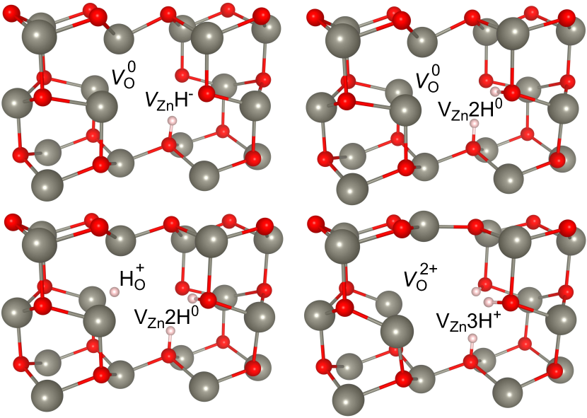
Figure 1 shows the formation energy of , , and hydrogenated divacancies with up to three hydrogen atoms as a function of the Fermi level position. Evidently, the divacancy is highly electrically active, displaying charge states ranging from to in the band gap. Interestingly, it seems to retain certain characteristics of its constituents; the thermodynamic charge-state transition levels in the lower part of the band gap are positioned close to the respective levels of the isolated , while those in the upper part exhibit negative-U characteristics similar to . These results can be understood by inspecting the electronic and atomic structure of the divacancy, as shown in Fig. 2. As a double donor, will transfer two electrons to , thus completely filling its defect states, so the charge-neutral divacancy can be viewed as a and pair. Starting from the neutral charge state, our calculations show that the divacancy can trap a hole polaron at one or two of the three O ions immediately adjacent to . The resulting (/) and (/) transition levels occur at 0.43 and 0.96 eV above the VBM. The charge state (with a hole polaron at each O ion) could not be stabilized.
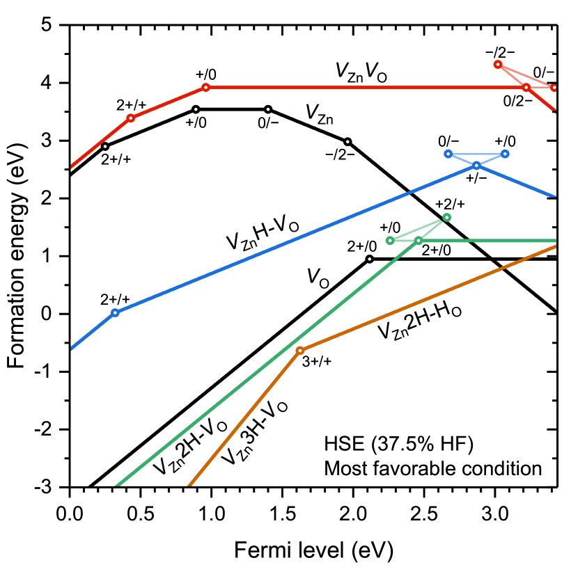
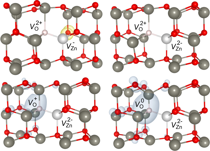
We also find that the charge-neutral divacancy can capture two electrons in a deep KS defect state (blue isosurfaces in Fig. 2) at . Notably, the thermodynamic charge-state transition occurs directly from to Chakrabarty and Patterson (2011). This is an important result, because it demonstrates that the isolated is not the only intrinsic defect exhibiting negative-U in ZnO, i.e., spectroscopic signatures indicating negative-U need not necessarily arise from the isolated only. The position of the (/) transition level of the divacancy is shifted strongly up towards the CB, relative to the (/) level of . This shift is mainly caused by the Coulomb repulsion between and the electrons occupying the state. Again, the negative-U behavior results from the large difference in local lattice relaxation around depending on the occupation of . The breathing-mode relaxation is inward by 15% for , whereas it is outward by 1% and 21% for and , respectively. Note that the relaxation is more inward for the divacancy compared to (Sec. III.1). Inward relaxation lowers the energy of the state, but increases the strain energy Janotti and Van de Walle (2007). For the divacancy, this energy balance is altered because the number of Zn ions immediately adjacent to is lowered from four to three. The calculated (/), (/) and (/) transition levels occur at 0.22, 0.42 and 0.02 eV below the CBM, respectively, resulting in 0.40 eV, which means the magnitude of U is lowered relative to the value for .
Holston et al. Holston et al. (2016) recently assigned a photo-EPR signal Leutwein and Schneider (1971) to the paramagnetic state () in neutron-irradiated ZnO, with the unpaired spin (hole polaron) residing primarily on one of the three O ions immediately adjacent to . Our prediction is in line with this result, i.e., we find that removing an electron from the neutral divacancy indeed produces a hole polaron at one of the three O ions associated with (the hole state corresponds to the yellow isosurface in Fig. 2). The same photo-EPR signal has also been observed in ZnO after 1.7, 2.5 and 3.0 MeV electron irradiation Schallenberger and Hausmann (1976); Soriano and Galland , i.e., for energies above the displacement threshold of both O (310 keV) and Zn (900 keV) in ZnO Locker and Meese (1972).
Although is thermodynamically unstable, it might be possible to create it in a metastable manner, e.g., by optical excitation. In fact, the analogous paramagnetic isolated state is detectable at low temperatures by photo-EPR Evans et al. (2008); Wang et al. (2009). Holston et al. Holston et al. (2016) initially envisioned the paramagnetic state as responsible for the aforementioned divacancy photo-EPR signal. However, this model was discarded as its EPR spectrum would have negative g shifts and well resolved hyperfine interactions with the adjacent 67Zn nuclei, similar to the isolated Holston et al. (2016). Moreover, seeing as the Fermi level was lowered by the neutron-irradiation Holston et al. (2016), the divacancies were most likely charge-neutral before illumination.
A pertinent question is whether divacancies are likely to form, and if they are stable at room temperature. Since and favor opposite conditions, the formation energy of is high, indicating a low equilibrium concentration. Indeed, experimentally, divacancies are typically observed in ZnO after post-growth processing, e.g., after irradiation, ion implantation, annealing or polishing Makkonen et al. (2016); Johansen et al. (2017); Holston et al. (2016). Regarding stability, we find that the defect reaction lowers the total energy by 0.83 eV under n-type conditions, which means that the divacancy will be stable at room temperature. Using the climbing nudged elastic band method Henkelman et al. (2000) and the Perdew-Burke-Ernzerhof (PBE) Perdew et al. (1996) functional, we have also investigated migration of the divacancy, i.e., nearest-neighbor Zn and O atoms hopping into the vacant Zn and O sites, respectively. The resulting migration barrier is about 1.2 eV, which is lower than those predicted previously for monovacancies in ZnO Janotti and Van de Walle (2007). Thus, divacancies may diffuse at relatively low temperatures and form larger vacancy clusters Bang et al. (2014) or other complexes Holston et al. (2016). Indeed, formation of vacancy clusters in ZnO has been reported in several experimental studies Makkonen et al. (2016); Johansen et al. (2017); Chan et al. (2013).
III.2.2 Dynamics of electron emission and capture
In order to allow comparison of our results with experimental data, e.g., energy level positions obtained by DLTS, we have constructed a CC diagram (shown in Fig. 3) describing the two-step process of electron emission from the doubly negatively charged divacancy to the CBM. The generalized coordinate (Q) along the horizontal axis corresponds to the mass-weighted atomic displacement between the equilibrium structure of for the three different charge states, namely , and Alkauskas et al. (2012), and can be loosely viewed as the magnitude of outward-breathing relaxation around . The total energy as a function of Q results in a potential energy curve for each charge state, and the energy is minimized at the equilibrium structure for each curve. The potential energy curves are displaced in energy along the vertical axis by the Fermi level position of the thermodynamic charge-state transition levels relative to the CBM, i.e., the difference in energy between the states in their equilibrium configurations. We will refer to these differences in energy as defect ionization energies () Wickramaratne et al. (2018).
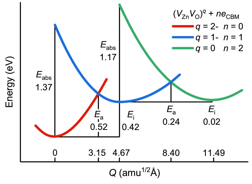
As shown in Fig. 3, we obtain an activation energy () of 0.52 eV for electron emission from to the CBM. This activation energy corresponds to the sum of and the capture barrier of 0.10 eV, which is taken as the energy required to reach the crossing point between the curves for and . Keep in mind that this barrier should be viewed as an upper estimate Mooney (1999); Wickramaratne et al. (2018). Moreover, the temperature effects described in Ref. Wickramaratne et al. (2018) are also neglected here. For emission from , we obtain a lower activation energy of 0.24 eV for emission and a capture barrier of 0.22 eV.
III.2.3 Optical transitions
Several broad luminescence bands have been observed in the visible part of the emission spectrum of ZnO, and there is a plethora of studies linking these to various point defects, including and . However, consensus is lacking and the defect origin of most bands remains unknown. Previous hybrid functional calculations suggest that the isolated vacancies are unlikely to give rise to luminescence in the visible range under n-type conditions Frodason et al. (2017); Lyons et al. (2017). However, the optical properties of the divacancy could be very different from those of and Lyons et al. (2017); Frodason et al. (2018).
We have considered three different optical transitions for the divacancy, namely hole capture from the VBM by and , and electron capture from the CBM by . Figure 4 shows the calculated CC diagrams for the two former transitions. Again, the potential energy curves in the CC diagrams are vertically displaced in energy by the Fermi level position of the respective thermodynamic charge-state transition levels relative to the VBM. In the context of luminescence, this is usually referred to as the zero phonon line energy, . In the Franck-Condon approximation, optical transitions take place without atomic motion, i.e., emission () and absorption () energies are given by the vertical arrows in Fig. 4. After an optical transition, the defect will relax to its equilibrium configuration by emitting phonons, losing the Franck-Condon relaxation energy (denoted for the ground state).
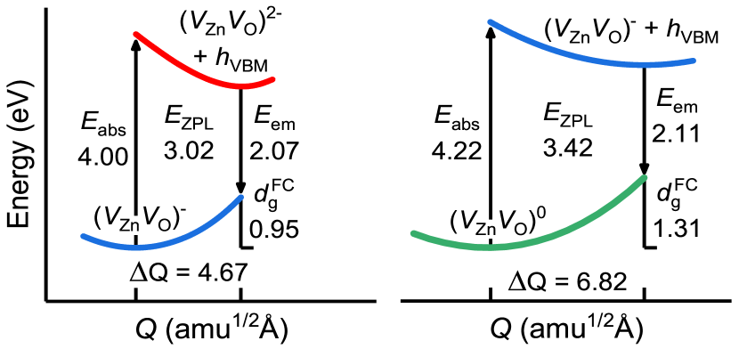
Interestingly, the difference in for the transitions in Fig. 4 is offset by a difference in , resulting in close emission energies of 2.07 and 2.11 eV. The capture of an electron at the CBM by the positively charged divacancy results in a lower emission energy of 1.66 eV; the CC diagram is not shown here, but is similar to what has been found previously for other related defects Frodason et al. (2017); Lyons et al. (2017); Frodason et al. (2018). Overall, our results show that the divacancy can give rise to broad luminescence peaking in the 1.6–2.1 eV range. We also note that both considered transitions should be dipole allowed. In the case of radiative electron capture the CB electrons have mostly Zn 4s character, while the final states have mostly O 2p Freysoldt et al. (2014) character. For radiative hole capture the initial state is a perturbed VB state which is composed mainly of O 2p states, while the defect state has mostly Zn 4s character. A different parity ensures a strong transition dipole moment and thus dipole-allowed transitions. Experimental studies on the optical properties of divacancies are scarce in the literature, but our calculations are consistent with the results reported by Dong et al. Dong et al. (2010). Based on cathodoluminescence and PAS data, Dong et al. Dong et al. (2010) suggested that the emission from large vacancy clusters peak at up to 2.1 eV, which shifts to lower energies with decreasing cluster size.
III.3 Hydrogen decorated divacancy
Besides being a ubiquitous impurity, hydrogen strongly influences the electrical and optical properties of ZnO, notably as a source of unintentional n-type conductivity Mollwo (1954); Thomas and Lander (1956); Van de Walle (2000). Interstitial hydrogen (H) acts exclusively as a donor by forming a strong O–H bond, preferably at the axial bond-centered site Van de Walle (2000); Wardle et al. (2005); Lavrov et al. (2009). However, H is mobile at room temperature Wardle et al. (2006); Johansen et al. (2008); Hupfer et al. (2017), and is thus likely to become trapped at defects. Importantly, the Coulomb attraction between H and results in highly stable complexes with , wherein H remains a donor by terminating O dangling bonds; the first two H atoms successively passivate the acceptor levels of , whereas the third transforms the complex into a shallow single donor. H can also be trapped at , but in this case the hydrogen behaves as an acceptor (H-) substituting for oxygen (fourfold coordinated). The resulting complex acts as a single shallow donor (H) Van de Walle and Janotti (2007); Lavrov et al. (2009).
Seeing as both and present potential trapping sites for H in the divacancy, different configurations were explored. Furthermore, to assess the divacancy as a hydrogen trap, removal energies were calculated as the difference in formation energy between the hydrogenated divacancy and the two remaining defects (calculated within separate supercells) when one H is removed and placed in its most stable isolated configuration ().
As shown in Fig. 5, the first two H atoms prefer to terminate O dangling bonds at , resulting in and complexes. The formation of these complexes lowers the total energy substantially, as evidenced by the large respective H removal energies of 2.84 and 2.02 eV. These are only slightly lower than for the and complexes Lyons et al. (2017). For comparison, removal energies of 2.08 and 1.26 eV are obtained for the and configurations. As indicated in Fig. 1, the location of the third H atom depends on the position of the Fermi level. When eV, the H atom will preferentially occupy , resulting in the complex with a calculated H removal energy of 1.26 eV. When eV, the H atom will instead terminate the final dangling bond at , resulting in . However, this latter configuration is unstable, as the H removal energy is 0.48 eV.
As can be seen in Fig. 1, the negative-U behavior persists for both and . However, the corresponding transition levels are shifted down in Fermi level position. Indeed, as the acceptor levels of are passivated by H, the Coulomb repulsion experienced by the electrons occupying the defect state is successively lowered, and the transition levels shift down towards the VB by 0.4 eV per H atom. Specifically, the (/) and (/) transition levels of and are predicted to occur at 0.57 and 0.98 eV below the CBM. The magnitude of U is unchanged with respect to the isolated divacancy (0.40 eV), which again indicates that it is mainly determined by the number of Zn atoms immediately adjacent to . Note that these trends hold for the (/) transition of the unstable complex as well. Lastly, the complex behaves like an effective-mass donor, and should be viewed as a and H pair. At this point, the divacancy is fully saturated with H atoms.
III.4 Comparison with DLTS and the E4 center
As previously discussed, the divacancy is not expected to be present in substantial amount in as grown samples, but may be formed during processing. Several electrically active defect centers having energy levels in the upper part of the band gap have been reported in n-type ZnO Monakhov et al. (2009). In this section, we compare our results for the divacancy with experimental DLTS data. We start by envisioning the electron emission from during a conventional DLTS measurement for n-type material. After a zero-bias filling pulse at low temperature, all divacancies will be filled with electrons. Subsequently, at some elevated temperature and under reverse bias, the first electron will be thermally emitted from with = 0.52 eV. Since the electron at is bound less strongly ( = 0.24 eV), emission of the second electron will proceed immediately after the first electron, leaving the defect in the state. For this reason, the divacancy will emit always two electrons during a conventional DLTS measurement, resulting in a single peak with = 0.52 eV. Indeed, such two-electron emission is common for centers where the electron binding energy shows an inverted order Hemmingsson et al. (1998); Son et al. (2012).
It is sometimes possible to obtain the activation energy associated with one-electron emission from a negative-U center by using DLTS with a short filling pulse and illumination. If the filling pulse is sufficiently short, most charge-neutral divacancies will be prevented from capturing more than one electron. A new DLTS peak, corresponding to the one-electron emission with = 0.24 eV, may then be observed at a lower temperature than for the two-electron emission. However, even with a short filling pulse, some divacancies may still capture a second electron, which means that they will be frozen out in the temperature range where the one-electron emission peak can be observed, and the peak will decrease to zero over time due to the repetitive pulses required by DLTS Hemmingsson et al. (1998). This can be avoided by optically “emptying” any divacancies having captured two electrons in the preceeding pulse before each filling pulse. This technique has been used, e.g., to observe one-electron emission from the negative-U center Z1/2 in 4H-SiC Hemmingsson et al. (1998).
Interestingly, the calculated = 0.52 eV for is close to the experimental activation energy of 0.55 eV for the E4 center in ZnO, which has been observed by several groups and is commonly assigned to a -related defect exhibiting negative-U Auret et al. (2001); Monakhov et al. (2009). However, theoretical predictions and experimental photo-EPR data Evans et al. (2008); Wang et al. (2009); Lyons et al. (2017) suggest that the isolated is substantially deeper than the E4 center, and this discrepancy has been a source for a long-standing debate in the community.
Our theoretical predictions for the divacancy conform to many of the experimental findings on the E4 center: (i) Negative-U behavior has been reported for E4 Frank et al. (2007); Ellguth et al. (2010). In particular, by using a short filling pulse and illumination as described above, an apparent energy level of 0.14 eV has been obtained for the one-electron emission from E4 Hofmann et al. (2007); Frank et al. (2007), which is close to our calculated value of 0.24 eV. (ii) Based on the temperature dependence of the rate of electron capture by E4 during the zero-bias filling pulse, Hupfer et al. Hupfer et al. (2016) obtained an experimental capture barrier of 0.15 eV, in good agreement with our calculated value of 0.22 eV for the divacancy. (iii) E4 exhibits a low concentration in as-grown material, but is prominent after He+ and H+ irradiation Auret et al. (2001); Hayes et al. (2007a, b); Hupfer et al. (2016). Its concentration hinges linearly on the ion dose, but amounts to only 0.23% of the total vacancy generation obtained from Monte Carlo simulations using the SRIM code Monakhov et al. (2009); Ziegler et al. (2010). Such a low generation rate is uncommon for a primary intrinsic defect, even if strong dynamic annealing is taken into account, and favors E4 as a high-order intrinsic defect such as the divacancy Monakhov et al. (2009). For comparison, the generation rate is about 1-2% for the divacancy in Si after high energy ion irradiation Monakhov et al. (2009). E4 has also been observed after 2 MeV electron irradiation Frank et al. (2007), i.e., above the displacement threshold of both O and Zn in ZnO. (iv) After H+ implantation at room temperature, the E4 center anneals out at a rate that fits well with a model invoking migration of H and subsequent reaction with E4 Hupfer et al. (2016); our results show that the divacancy has a strong affinity for H, similar to that of . Furthermore, E4 is accompanied by a second trap labelled Ep2 after H+ irradiation, which similarly exhibits a low introduction rate Auret et al. (2001). Indeed, Auret et al. Auret et al. (2001) suggested that Ep1 (E4) and Ep2 might be high-order rather than primary intrinsic defects. Finally, Ep2 has an apparent energy level at 0.78 eV, which incidentally fits well with our calculated ionization energy of 0.77 eV for .
IV Conclusion
Using hybrid functional calculations, we have investigated the divacancy in ZnO. The divacancy is predicted to be a highly electrically active defect, exhibiting charge states ranging from to in the band gap. Interestingly, it retains both the negative-U behavior of and the polaronic nature of . The former result is of particular interest, as it demonstrates that the isolated is not the only intrinsic defect exhibiting negative-U in ZnO. We have also studied the interaction between divacancies and H, and find that the divacancy can accommodate up to three H atoms, the first two of which prefer to terminate O dangling bonds at . Based on comparison of our results with experimental DLTS data in the literature Monakhov et al. (2009); Auret et al. (2001); Hayes et al. (2007a, b); Ellguth et al. (2010); Frank et al. (2007), is proposed as a potential origin of the E4 center, which is commonly associated with a -related defect with negative-U.
Acknowledgements.
Financial support was kindly provided by the Research Council of Norway and University of Oslo through the frontier research project FUNDAMeNT (no. 251131, FriPro ToppForsk-program). A.A. was supported by Marie Skłodowska-Curie Action of the European Union (project Nitride-SRH, Grant No. 657054). The computations were performed on resources provided by UNINETT Sigma2 - the National Infrastructure for High Performance Computing and Data Storage in Norway.References
- Janotti and de Walle (2009) A. Janotti and C. G. V. de Walle, Rep. Prog. Phys. 72, 126501 (2009).
- Janotti and Van de Walle (2007) A. Janotti and C. G. Van de Walle, Phys. Rev. B 76, 165202 (2007).
- Chen and Pasquarello (2017) W. Chen and A. Pasquarello, Phys. Rev. B 96, 020101 (2017).
- Miceli et al. (2018) G. Miceli, W. Chen, I. Reshetnyak, and A. Pasquarello, Phys. Rev. B 97, 121112 (2018).
- Oba et al. (2008) F. Oba, A. Togo, I. Tanaka, J. Paier, and G. Kresse, Phys. Rev. B 77, 245202 (2008).
- Alkauskas and Pasquarello (2011) A. Alkauskas and A. Pasquarello, Phys. Rev. B 84, 125206 (2011).
- Clark et al. (2010) S. J. Clark, J. Robertson, S. Lany, and A. Zunger, Phys. Rev. B 81, 115311 (2010).
- Lany and Zunger (2010) S. Lany and A. Zunger, Phys. Rev. B 81, 113201 (2010).
- Anderson (1975) P. W. Anderson, Phys. Rev. Lett. 34, 953 (1975).
- Lany and Zunger (2009) S. Lany and A. Zunger, Phys. Rev. B 80, 085202 (2009).
- Bjørheim et al. (2012) T. S. Bjørheim, S. Erdal, K. M. Johansen, K. E. Knutsen, and T. Norby, J. Phys. Chem. C 116, 23764 (2012).
- Petretto and Bruneval (2015) G. Petretto and F. Bruneval, Phys. Rev. B 92, 224111 (2015).
- Frodason et al. (2017) Y. K. Frodason, K. M. Johansen, T. S. Bjørheim, B. G. Svensson, and A. Alkauskas, Phys. Rev. B 95, 094105 (2017).
- Lyons et al. (2017) J. L. Lyons, J. B. Varley, D. Steiauf, A. Janotti, and C. G. V. de Walle, J. Appl. Phys. 122, 035704 (2017).
- Makkonen et al. (2016) I. Makkonen, E. Korhonen, V. Prozheeva, and F. Tuomisto, J. Phys. Condens. Matter 28, 224002 (2016).
- Johansen et al. (2017) K. Johansen, F. Tuomisto, I. Makkonen, and L. Vines, Mat. Sci. Semicon. Proc. 69, 23 (2017).
- Holston et al. (2016) M. S. Holston, E. M. Golden, B. E. Kananen, J. W. McClory, N. C. Giles, and L. E. Halliburton, J. Appl. Phys. 119, 145701 (2016).
- Vidya et al. (2011) R. Vidya, P. Ravindran, H. Fjellvåg, B. G. Svensson, E. Monakhov, M. Ganchenkova, and R. M. Nieminen, Phys. Rev. B 83, 045206 (2011).
- Bang et al. (2014) J. Bang, Y.-S. Kim, C. H. Park, F. Gao, and S. B. Zhang, Appl. Phys. Lett. 104, 252101 (2014).
- Chakrabarty and Patterson (2011) A. Chakrabarty and C. H. Patterson, Phys. Rev. B 84, 054441 (2011).
- Chakrabarty and Patterson (2012) A. Chakrabarty and C. H. Patterson, J. Chem. Phys. 137, 054709 (2012).
- Shin and Kim (2014) E.-H. Shin and H. Kim, J. Korean Phys. Soc. 64, 543 (2014).
- Krukau et al. (2006) A. V. Krukau, O. A. Vydrov, A. F. Izmaylov, and G. E. Scuseria, J. Chem. Phys. 125, 224106 (2006).
- Blöchl (1994) P. E. Blöchl, Phys. Rev. B 50, 17953 (1994).
- Kresse and Hafner (1994) G. Kresse and J. Hafner, J. Phys-Condens. Mat. 6, 8245 (1994).
- Kresse and Joubert (1999) G. Kresse and D. Joubert, Phys. Rev. B 59, 1758 (1999).
- Kresse and Hafner (1993) G. Kresse and J. Hafner, Phys. Rev. B 47, 558 (1993).
- Kresse and Furthmüller (1996) G. Kresse and J. Furthmüller, Phys. Rev. B 54, 11169 (1996).
- Oba et al. (2011) F. Oba, M. Choi, A. Togo, and I. Tanaka, Sci. Technol. Adv. Mater. 12, 034302 (2011).
- Freysoldt et al. (2014) C. Freysoldt, B. Grabowski, T. Hickel, J. Neugebauer, G. Kresse, A. Janotti, and C. G. Van de Walle, Rev. Mod. Phys. 86, 253 (2014).
- Zhang and Northrup (1991) S. B. Zhang and J. E. Northrup, Phys. Rev. Lett. 67, 2339 (1991).
- Kumagai and Oba (2014) Y. Kumagai and F. Oba, Phys. Rev. B 89, 195205 (2014).
- Freysoldt et al. (2009) C. Freysoldt, J. Neugebauer, and C. G. Van de Walle, Phys. Rev. Lett. 102, 016402 (2009).
- Komsa et al. (2012) H.-P. Komsa, T. T. Rantala, and A. Pasquarello, Phys. Rev. B 86, 045112 (2012).
- Stoneham and Sangster (1983) A. M. Stoneham and M. J. L. Sangster, Radiation Effects 73, 267 (1983), https://doi.org/10.1080/00337578308220683 .
- Alkauskas et al. (2012) A. Alkauskas, J. L. Lyons, D. Steiauf, and C. G. Van de Walle, Phys. Rev. Lett. 109, 267401 (2012).
- Wickramaratne et al. (2018) D. Wickramaratne, C. E. Dreyer, B. Monserrat, J.-X. Shen, J. L. Lyons, A. Alkauskas, and C. G. Van de Walle, Appl. Phys. Lett. 113, 192106 (2018).
- Van de Walle and Neugebauer (2004) C. G. Van de Walle and J. Neugebauer, J. Appl. Phys. 95, 3851 (2004).
- Evans et al. (2008) S. M. Evans, N. C. Giles, L. E. Halliburton, and L. A. Kappers, J. Appl. Phys. 103, 043710 (2008).
- Wang et al. (2009) X. J. Wang, L. S. Vlasenko, S. J. Pearton, W. M. Chen, and I. A. Buyanova, J. Phys. D Appl. Phys. 42, 175411 (2009).
- Lany and Zunger (2007) S. Lany and A. Zunger, Phys. Rev. Lett. 98, 045501 (2007).
- Galland and Herve (1970) D. Galland and A. Herve, Phys. Lett. A 33, 1 (1970).
- Leutwein and Schneider (1971) K. Leutwein and J. Schneider, Z. Naturforsch. A 26, 1236 (1971).
- Schallenberger and Hausmann (1976) B. Schallenberger and A. Hausmann, Z Phys. B Condens. Matter 23, 177 (1976).
- (45) V. Soriano and D. Galland, Phys. Status Solidi B 77, 739.
- Locker and Meese (1972) D. R. Locker and J. M. Meese, IEEE Trans. Nucl. Sci. 19, 237 (1972).
- Henkelman et al. (2000) G. Henkelman, B. P. Uberuaga, and H. Jansson, The Journal of Chemical Physics 113, 9901 (2000).
- Perdew et al. (1996) J. P. Perdew, K. Burke, and M. Ernzerhof, Phys. Rev. Lett. 77, 3865 (1996).
- Chan et al. (2013) K. S. Chan, L. Vines, K. M. Johansen, E. V. Monakhov, J. D. Ye, P. Parkinson, C. Jagadish, B. G. Svensson, and J. Wong-Leung, J. Appl. Phys. 114, 083111 (2013).
- Mooney (1999) P. Mooney, in Identification of Defects in Semiconductors, Semiconductors and Semimetals, Vol. 51, edited by M. Stavola (Elsevier, 1999) pp. 93 – 152.
- Frodason et al. (2018) Y. K. Frodason, K. M. Johansen, T. S. Bjørheim, B. G. Svensson, and A. Alkauskas, Phys. Rev. B 97, 104109 (2018).
- Dong et al. (2010) Y. Dong, F. Tuomisto, B. G. Svensson, A. Yu. Kuznetsov, and L. J. Brillson, Phys. Rev. B 81, 081201 (2010).
- Mollwo (1954) E. Mollwo, Z. Phys. A 138, 478 (1954).
- Thomas and Lander (1956) D. G. Thomas and J. J. Lander, J. Chem. Phys. 25, 1136 (1956).
- Van de Walle (2000) C. G. Van de Walle, Phys. Rev. Lett. 85, 1012 (2000).
- Wardle et al. (2005) M. G. Wardle, J. P. Goss, and P. R. Briddon, Phys. Rev. B 72, 155108 (2005).
- Lavrov et al. (2009) E. V. Lavrov, F. Herklotz, and J. Weber, Phys. Rev. B 79, 165210 (2009).
- Wardle et al. (2006) M. G. Wardle, J. P. Goss, and P. R. Briddon, Phys. Rev. Lett. 96, 205504 (2006).
- Johansen et al. (2008) K. M. Johansen, J. S. Christensen, E. V. Monakhov, A. Y. Kuznetsov, and B. G. Svensson, Appl. Phys. Lett. 93, 152109 (2008).
- Hupfer et al. (2017) A. Hupfer, C. Bhoodoo, L. Vines, and B. G. Svensson, Mat. Sci. Semicon. Proc. 69, 13 (2017).
- Van de Walle and Janotti (2007) C. G. Van de Walle and A. Janotti, Nat. Mater. 6, 44 (2007).
- Monakhov et al. (2009) E. V. Monakhov, A. Y. Kuznetsov, and B. G. Svensson, J. Phys. D. Appl. Phys. 42, 153001 (2009).
- Hemmingsson et al. (1998) C. G. Hemmingsson, N. T. Son, A. Ellison, J. Zhang, and E. Janzén, Phys. Rev. B 58, R10119 (1998).
- Son et al. (2012) N. T. Son, X. T. Trinh, L. S. Løvlie, B. G. Svensson, K. Kawahara, J. Suda, T. Kimoto, T. Umeda, J. Isoya, T. Makino, T. Ohshima, and E. Janzén, Phys. Rev. Lett. 109, 187603 (2012).
- Auret et al. (2001) F. D. Auret, S. A. Goodman, M. Hayes, M. J. Legodi, H. A. van Laarhoven, and D. C. Look, Appl. Phys. Lett. 79, 3074 (2001).
- Frank et al. (2007) T. Frank, G. Pensl, R. Tena-Zaera, J. Zúñiga-Pérez, C. Martínez-Tomás, V. Muñoz-Sanjosé, T. Ohshima, H. Itoh, D. Hofmann, D. Pfisterer, J. Sann, and B. Meyer, Appl. Phys. A 88, 141 (2007).
- Ellguth et al. (2010) M. Ellguth, M. Schmidt, R. Pickenhain, H. V. Wenckstern, and M. Grundmann, Phys. Status Solidi B 248, 941 (2010).
- Hofmann et al. (2007) D. Hofmann, D. Pfisterer, J. Sann, B. Meyer, R. Tena-Zaera, V. Munoz-Sanjose, T. Frank, and G. Pensl, Appl. Phys. A 88, 147 (2007).
- Hupfer et al. (2016) A. Hupfer, C. Bhoodoo, L. Vines, and B. G. Svensson, J. Appl. Phys. 119, 181506 (2016).
- Hayes et al. (2007a) M. Hayes, F. Auret, P. J. van Rensburg, J. Nel, W. Wesch, and E. Wendler, Nucl . Instrum. Method B 257, 311 (2007a).
- Hayes et al. (2007b) M. Hayes, F. D. Auret, P. J. Janse van Rensburg, J. M. Nel, W. Wesch, and E. Wendler, Phys. Status Solidi B 244, 1544 (2007b).
- Ziegler et al. (2010) J. F. Ziegler, M. Ziegler, and J. Biersack, Nucl. Instrum. Method B 268, 1818 (2010).