Terahertz Laser Combs in Graphene Field-Effect Transistors
Abstract
Electrically injected terahertz (THz) radiation sources are extremely appealing given their versatility and miniaturization potential, opening the venue for integrated-circuit THz technology. In this work, we show that coherent THz frequency combs in the range can be generated making use of graphene plasmonics. Our setup consists of a graphene field-effect transistor with asymmetric boundary conditions, with the radiation originating from a plasmonic instability that can be controlled by direct current injection. We put forward a combined analytical and numerical analysis of the graphene plasma hydrodynamics, showing that the instability can be experimentally controlled by the applied gate voltage and the injected current. Our calculations indicate that the emitted THz comb exhibits appreciable temporal coherence () and radiant emittance (). This makes our scheme an appealing candidate for a graphene-base THz laser source. Moreover, a mechanism for the instability amplification is advanced for the case of substrates with varying electric permitivitty, which allows to overcome eventual limitations associated with the experimental implementation.
Introduction.Terahertz (THz) radiation consists of electromagnetic (EM) waves within the frequency range from 0.1 to 10 THz, filling the gap between microwave and infrared light. The technology for its production is currently a very active field of research Williams (2007); edi (2013), since THz radiation has numerous applications, comprising sensing, imaging, metrology and spectroscopy Woolard et al. (2003); Pornsuwancharoen et al. (2013). A major reason for the hype around THz radiation is that fact that it is able to penetrate several materials that are opaque to visible and IR radiation, while the short wavelength provides high image resolution (Stantchev et al., 2017). On the other hand the attenuation in water can provide information for medical imaging while being non-ionising and biologically safe.
Among all forms of THz radiation, THz laser (THL) combs play a prominent role within such technology Füser and Bieler (2014); Barmes et al. (2013). However, THL generation still faces significant difficulties, being restricted to gas lasers Dai et al. (2011); Dai and Zhang (2009), with low efficiency, quantum cascade lasers Burghoff et al. (2014); Williams (2007), which require extremely low temperatures, and free electron lasers Tan et al. (2012), practically impossible to miniaturize. With the advent of graphene plasmonics, new techniques relying in optical pumping have been put forward Altares Menendez and Maes (2017); Otsuji et al. (2013, 2014). The progress in graphene based transistors Schwierz (2010) paved the way to the possibility for all-electrical miniaturized devices for low power radiation emission and detection. Yet, such integrated-circuit THz technology based on graphene is at its infancy, notwithstanding some experimental studies in visible and mid-infrared light emission Kim et al. (2015, 2018); Beltaos et al. (2017). More recently, THz emission from dual gate graphene field-effect transistor (FET) due to electron/hole recombination in a p-i-n junction has been made possible Yadav et al. (2017, 2018). Practical solutions towards inexpensive, compact and easy-to-operate lasing devices are, therefore, desirable.
In this Letter, we exploit a scheme for the generation of coherent THz frequency combs in graphene field-effect transistors, arising from the Dyakonov-Shur (DS) plasmonic instability Dyakonov and Shur (1993); Kargar et al. (2018). The latter can be excited via the injection of an electric current, thus forgoing the necessity of optical pumping. This opens the possibility to the development of an all-electric, low-consumption stimulated THL, capable of operating at room temperature. Our calculations are based on the hydrodynamic formulation of the plasma in monolayer graphene, from which we analytically obtain the instability criteria and numerically extract the radiation spectrum, intensity and correlation. Our findings reveal that the emitted THL comb exhibits appreciably large values of both spatial and temporal coherences, suggesting our scheme to be a competitive solution towards THz laser light with integrated-circuit technology. Finally, a new passive mechanism for the amplification of the DS instability in gated graphene is introduced.

Graphene plasma instability.The dynamics of the electronic flow in a graphene FET can be described with the help of a hydrodynamic model Chaves et al. (2017); Müller et al. (2009); Svintsov et al. (2013). Assuming the transport to be restricted to one (say ) direction, the latter reads
| (1) |
where is the 2D electronic density, is the flow velocity, is the total force exerted in the electrons, is the pressure (with denoting the Fermi speed), and the electron effective mass. The validity of the hydrodynamic model in Eq. (1) is granted thanks to the large value of the mean free path of electron scattering with phonons and impurities at room temperature (), thus assuring that ballistic transport holds. We also consider graphene to be in the degenerate Fermi liquid regime, provided that the Fermi level remains bellow the Van Hove singularities. At room temperature, the latter holds for Fermi energies in the range .
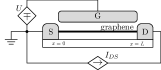
The fact that electrons in graphene behave as massless fermions poses a difficulty to the development of hydrodynamic models with explicit dependency on the mass. Here, the Drude mass , with denoting the equilibrium carrier density, is used as an effective mass Svintsov et al. (2013); Castro Neto et al. (2009); Chaves et al. (2017). In the field-effect transistor (FET) configuration comprising a drain, a source and a gate (see Fig. 1a for a schematic representation), the electric force exerted on the electrons is dominated by the external potential that screens Coulomb interaction. The applied bias potential has the contribution of both the parallel plate capacitance (with denoting the distance between the gate and the graphene sheet) and the quantum capacitance Zhu et al. (2009); Fang et al. (2007); Dröscher et al. (2012); Das Sarma et al. (2011) , as
| (2) |
For carrier densities in the range , quantum capacity dominates, and the potential can be approximated as . Keeping the pressure term up to first order in the density, the fluid model in (1) can be recast in a dimensionless form as
| (3) |
where is the electron mean drift velocity along the graphene channel and can be interpreted as sound velocity of the carriers fluid, as the dispersion relation for the electron fluctuations, , is similar to that of a shallow water. For typical values, the ratio scales up to a few tens.
The hydrodynamic model in Eq. (3) contains an instability under the boundary conditions of fixed density at source and fixed current density at the drain , dubbed in the literature as the Dyakonov-Shur (DS) instability Dyakonov and Shur (1993); Dyakonov (2011). The later arises from the multiple reflections of the plasma waves at the boundaries, which provides a positive feedback for the incoming waves driven by the current at the drain. Combining Eq. (3) with the asymmetric boundary conditions described above, the dispersion relation becomes complex, , where is the electron oscillation frequency and is the instability growth rate Dyakonov and Shur (1993); Dmitriev et al. (1997); Crowne (1997)
| (4) |
Therefore, given the dependence of with gate voltage, and as , with representing the source-to-drain current and the transverse width of the sheet, the frequency can be tuned by the gate voltage and injected drain current, not being solely restricted to the geometric factors of the FET.


After an initial transient time, the DS instability saturates due to the nonlinearities and the system goes in a cycle of shock and rarefaction waves that sustain the collective motion of the electrons (see Fig. 1b). Evidently, such collective oscillation radiates in the same main frequency that lies in the THz range for typical values of parameters, as depicted in Fig. 2. Moreover, as the electrons are transported along density shock waves, they bunch together and behave as a macroscopic dipole. As a consequence, the emitted radiation is highly coherent, a fact that we will demonstrate below and that we believe to be at the basis of a THL source.
In experimental conditions, the ideal situation described above must be analysed with care. Indeed, for the DS instability to take place, the growth rate has to be larger than the total relaxation rate, , due to scattering with impurities and phonons. Recent experiments performed at room temperature point to an electron mobility of monolayer suspended graphene of Bolotin et al. (2008); Zhu et al. (2009), that results in an average relaxation rate . Fortunately, for a suitable choice of parameters, we can safely operate in the regime , as shown in Fig. 2.
Numerical simulation of the THz frequency comb.The hyperbolic set of fluid equations in (3) have been integrated using a second-order (time and space) Richtmyer two-step Lax-Wendroff scheme LeVeque (1992). The suppression of numerical oscillations at the shock front has been implemented by means of a moving average filter on the spatial domain, from which the and profiles are obtained as well as the integrated current and tension drop across the FET. From the output current and density, the electromagnetic field can then be calculated from Jefimenko’s integral equations Griffiths and Heald (1991)
| (5) |
with being the displacement vector and the speed of light. The direct integration of Eq. (5) allows the reconstruction of the emitted fields both in near field and far field regimes.

For the latter, our calculations provide a radiant emittance of the order of . The reconstructed radiation pattern of the graphene layer (i.e. without the reckoning radiation reflection/absorption effects due to the metallic gate, an approximation that holds as the ratio , implying the radiation wavelength to be much larger that the typical FET dimensions), shows a wide omnidirectional profile with a half-power beam width of , as patent in Fig. 3. In fact, the angular Poynting vector profile is , unlike the typical dipolar emitter . Such a wide lobe profile can be explained by the fact that the collective movement of charges occurs on the entire area of the graphene FET, similarly to patch antennae Kobayashi (2016). The radiated spectrum consists of a frequency comb in the THz range, with frequencies with , as can be seen in the inset of Fig. 4. Hereafter, a suitable design of a resonance cavity would allow the selection and amplification of the desired mode. Furthermore, if a periodic inversion of polarity is imposed across the channel, in such a way that after the saturation time the perturbation due to DS instability decays, a train of short pulses can be formed. This can be implemented with a pulse generator controlling the injected current at drain with a repetition rate . In Fourier space, such pulses form a THz frequency comb around the main frequency with frequencies given by with as seen in Fig. 4.

THz laser coherences.In order to determine wether or not the emitted radiation can be understood as a THz laser, we proceed to the calculation of both the temporal and spatial coherences Born and Wolf (1980),
| (6) |
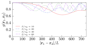
As expected, the radiated field exhibits appreciably large coherences, both in far field and near field (not shown) regimes, that increase with , as presented in Fig. 5. As mentioned above, such an appreciable coherence degree is attributed to the collective motion of the electrons bunching together in the shock and rarefaction waves cycle. The observed oscillation in the temporal coherence is due to the frequency mixing in the frequency comb, a feature that could be suppressed with the help of a THz cavity, allowing for mode selection in the THz comb.

Improving the DS instability.As mentioned above, one possible limitation of our process may arise when we approach the threshold region . To circumvent this issue without changing the setup, we found that by varying the speed of the the plasma waves along the channel length, i.e. by taking (either by manipulating the permittivity or the gate distance ), a remarkable enhancement of the instability growth rate can be achieved, while no significant impact on the spectrum is observable. Such modification on the velocity along the FET channel introduces a positive feedback in the current instability, which leads to a larger value of the growth rate and, consequently, to a faster saturation of the DS instability. This features are illustrated in Fig. 6. As such, the electron density at saturation is higher, resulting in a increase in the emitted power for . The numerically extracted valued of the growth rate in the speed-gradient scheme, , are significantly larger than in Eq. (4), as it can be stated in Table 1. This mechanism can be seen as analogous to wave shoaling effect on shallow waters systems and the shock wave amplitude is likewise amplified in the presence of the velocity gradient Gourlay (2011). Although out of the scope of the present work, the investigation of the DS mechanism in combination with other positive feedback configurations, such as subtract patterning Zolotovskii et al. (2018) and counter flows Morgado and Silveirinha (2017), will certainly deserve our attention in the near future.

| 20 | 40 | 60 | 80 | |
|---|---|---|---|---|
| 0.025 | ||||
| 0.05 | ||||
| 0.075 | ||||
| 0.1 | ||||
Conclusion.We make use of a hydrodynamic model to describe a plasmonic instability (Dyakonov-Shur instability) taking place in a graphene field-effect transistor at room temperature. Our scheme, based on the control of the electron current at the transistor drain, results in the emission of a THz frequency comb. Numerical simulations suggest that the emitted THz radiation is extremely coherent, thus be an appealing candidate for a THz laser source. Our findings point towards a method for the development of tuneable, all-electrical THz antennae, dismissing the usage of external light sources such as THz solutions based on quantum cascade lasers. This puts graphene plasmonics and, in particular, graphene field-effect transistors in the run for competitive, low-consumption THz devices based on integrated-circuit technology, allowing the fabrication of patch arrays designed to enhance the total radiated power.
Additional effects can be taken into account, such as the electron-phonon coupling. This can particularly important in the case of suspended graphene, as the out-of-plane vibrations (flexural phonons) play a significant role in the electron transport Castro et al. (2010). Moreover, important effect related to electron viscosity may arise in thin graphene ribbons Tomadin et al. (2014). The later, more relevant for very small devices, may hinder the plasmonic instability and, for that reason, it is desirable to combine the Dyakonov-Shur configuration with other positive-feedback schemes. Finally, the instability amplification by resonances taking place in magnetized graphene plasmas may also conduct to interesting solutions Chen (2012).
One of the authors (H.T.) acknowledges Fundação da Ciência e Tecnologia (FCT-Portugal) through the grant number IF/00433/2015.
References
- Williams (2007) B. S. Williams, Nature Photonics 1, 517 (2007).
- edi (2013) Nature Photonics 7, 665 (2013).
- Woolard et al. (2003) D. L. Woolard, W. R. Loerop, and M. S. Shur, eds., Terahertz sensing technology Volume 2: Emerging Scientific Applications & Novel Device Concepts (World Scientific, 2003).
- Pornsuwancharoen et al. (2013) N. Pornsuwancharoen, M. Tasakorn, P. P. Yupapin, and S. Chaiyasoonthorn, Optik 124, 446 (2013).
- Stantchev et al. (2017) R. I. Stantchev, D. B. Phillips, P. Hobson, S. M. Hornett, M. J. Padgett, and E. Hendry, Optica 4, 989 (2017).
- Füser and Bieler (2014) H. Füser and M. Bieler, Journal of Infrared, Millimeter, and Terahertz Waves 35, 585 (2014).
- Barmes et al. (2013) I. Barmes, S. Witte, and K. S. E. Eikema, Nature Photonics 7, 38 (2013).
- Dai et al. (2011) J. Dai, J. Liu, and X.-C. Zhang, IEEE Journal of Selected Topics in Quantum Electronics 17, 183 (2011).
- Dai and Zhang (2009) J. Dai and X.-C. Zhang, Applied Physics Letters 94, 021117 (2009).
- Burghoff et al. (2014) D. Burghoff, T.-y. Kao, N. Han, C. W. I. Chan, X. Cai, Y. Yang, D. J. Hayton, J.-r. Gao, J. L. Reno, and Q. Hu, Nature Photonics 8, 462 (2014).
- Tan et al. (2012) P. Tan, J. Huang, K. Liu, Y. Xiong, and M. Fan, Science China Information Sciences 55, 1 (2012).
- Altares Menendez and Maes (2017) G. Altares Menendez and B. Maes, Physical Review B 95, 144307 (2017).
- Otsuji et al. (2013) T. Otsuji, S. B. Tombet, A. Satou, M. Ryzhii, and V. Ryzhii, IEEE Journal of Selected Topics in Quantum Electronics 19, 8400209 (2013).
- Otsuji et al. (2014) T. Otsuji, A. Satou, M. Ryzhii, V. Popov, V. Mitin, and V. Ryzhii, Journal of Physics: Conference Series 486, 012007 (2014).
- Schwierz (2010) F. Schwierz, Nature Nanotechnology 5, 487 (2010).
- Kim et al. (2015) Y. S. Y. D. Kim, H. Kim, Y. Cho, J. H. Ryoo, C.-H. Park, P. Kim, Y. S. Y. D. Kim, S. S. W. Lee, Y. Li, S.-N. Park, Y. Shim Yoo, D. Yoon, V. E. Dorgan, E. Pop, T. F. Heinz, J. Hone, S.-H. Chun, H. Cheong, S. S. W. Lee, M.-H. Bae, and Y. D. Park, Nature Nanotechnology 10, 676 (2015).
- Kim et al. (2018) Y. D. Kim, Y. Gao, R.-J. Shiue, L. Wang, O. B. Aslan, M.-H. Bae, H. Kim, D. Seo, H.-J. Choi, S. H. Kim, A. Nemilentsau, T. Low, C. Tan, D. K. Efetov, T. Taniguchi, K. Watanabe, K. L. Shepard, T. F. Heinz, D. Englund, J. Hone, Y. D. Kim, H.-J. Choi, Y. Gao, O. B. Aslan, L. Wang, H. Kim, T. F. Heinz, J. Hone, M.-H. Bae, S. H. Kim, D. K. Efetov, K. L. Shepard, D. Englund, T. Taniguchi, A. Nemilentsau, T. Low, R.-J. Shiue, L. Wang, O. B. Aslan, M.-H. Bae, H. Kim, D. Seo, H.-J. Choi, S. H. Kim, A. Nemilentsau, T. Low, C. Tan, D. K. Efetov, T. Taniguchi, K. Watanabe, K. L. Shepard, T. F. Heinz, D. Englund, and J. Hone, Nano Letters 18, 934 (2018).
- Beltaos et al. (2017) A. Beltaos, A. J. Bergren, K. Bosnick, N. Pekas, S. Lane, K. Cui, A. Matković, A. Meldrum, K. Bosnick, K. Cui, A. J. Bergren, A. Beltaos, S. Lane, A. Matković, A. J. Bergren, K. Bosnick, N. Pekas, S. Lane, K. Cui, A. Matković, and A. Meldrum, Nano Futures 1, 025004 (2017).
- Yadav et al. (2017) D. Yadav, Y. Tobah, J. Mitsushio, G. Tamamushi, T. Watanabe, A. A. Dubinov, M. Ryzhii, V. Ryzhii, and T. Otsuji, in Conference on Lasers and Electro-Optics (OSA, Washington, D.C., 2017) p. AM2B.7.
- Yadav et al. (2018) D. Yadav, G. Tamamushi, T. Watanabe, J. Mitsushio, Y. Tobah, K. Sugawara, A. A. Dubinov, A. Satou, M. Ryzhii, V. Ryzhii, and T. Otsuji, Nanophotonics 7, 741 (2018).
- Dyakonov and Shur (1993) M. Dyakonov and M. Shur, Physical Review Letters 71, 2465 (1993).
- Kargar et al. (2018) Z. Kargar, T. Linn, and C. Jungemann, Semiconductor Science and Technology 33 (2018).
- Chaves et al. (2017) A. J. Chaves, N. M. Peres, G. Smirnov, and N. Asger Mortensen, Physical Review B 96, 1 (2017).
- Müller et al. (2009) M. Müller, J. Schmalian, and L. Fritz, Physical Review Letters 103, 025301 (2009).
- Svintsov et al. (2013) D. Svintsov, V. Vyurkov, V. Ryzhii, and T. Otsuji, Physical Review B - Condensed Matter and Materials Physics 88, 28 (2013).
- Castro Neto et al. (2009) A. H. Castro Neto, F. Guinea, N. M. R. Peres, K. S. Novoselov, and A. K. Geim, Reviews of Modern Physics 81, 109 (2009).
- Zhu et al. (2009) W. Zhu, V. Perebeinos, M. Freitag, and P. Avouris, Physical Review B 80, 235402 (2009).
- Fang et al. (2007) T. Fang, A. Konar, H. Xing, and D. Jena, Applied Physics Letters 91, 2007 (2007).
- Dröscher et al. (2012) S. Dröscher, P. Roulleau, F. Molitor, P. Studerus, C. Stampfer, K. Ensslin, and T. Ihn, Physica Scripta T146, 014009 (2012).
- Das Sarma et al. (2011) S. Das Sarma, S. Adam, E. H. Hwang, and E. Rossi, Reviews of Modern Physics 83, 407 (2011).
- Dyakonov (2011) M. Dyakonov, Comptes Rendus Physique 11, 10 (2011).
- Dmitriev et al. (1997) A. P. Dmitriev, A. S. Furman, V. Y. Kachorovskii, G. G. Samsonidze, and G. G. Samsonidze, Physical Review B 55, 10319 (1997).
- Crowne (1997) F. J. Crowne, Journal of Applied Physics 82, 1242 (1997).
- Bolotin et al. (2008) K. I. Bolotin, K. J. Sikes, Z. Jiang, M. Klima, G. Fudenberg, J. Hone, P. Kim, and H. L. Stormer, Solid State Communications 146, 351 (2008).
- LeVeque (1992) R. J. LeVeque, Lectures in Mathematics ETH Zürich, 2nd ed. (Birkhauser Verlag, Boston, 1992).
- Griffiths and Heald (1991) D. J. Griffiths and M. A. Heald, American Journal of Physics 59, 111 (1991).
- Kobayashi (2016) H. Kobayashi, in 2016 URSI International Symposium on Electromagnetic Theory (EMTS) (IEEE, 2016).
- Frigo and Johnson (2005) M. Frigo and S. Johnson, Proceedings of the IEEE 93, 216 (2005).
- Born and Wolf (1980) M. Born and E. Wolf, Principles of Optics: Electromagnetic Theory of Propagation, Interference and Diffraction of Light, 6th ed. (Pergamon, 1980).
- Gourlay (2011) M. R. Gourlay, Encyclopedia of Modern Coral Reefs: Structure, Form and Process, edited by D. Hopley (Springer Netherlands, 2011).
- Zolotovskii et al. (2018) I. O. Zolotovskii, Y. S. Dadoenkova, S. G. Moiseev, A. S. Kadochkin, V. V. Svetukhin, and A. A. Fotiadi, Phys. Rev. A 97, 053828 (2018).
- Morgado and Silveirinha (2017) T. A. Morgado and M. G. Silveirinha, Phys. Rev. Lett. 119, 133901 (2017).
- Castro et al. (2010) E. V. Castro, H. Ochoa, M. I. Katsnelson, R. V. Gorbachev, D. C. Elias, K. S. Novoselov, A. K. Geim, and F. Guinea, Physical Review Letters 105, 266601 (2010).
- Tomadin et al. (2014) A. Tomadin, G. Vignale, and M. Polini, Phys. Rev. Lett. 113, 235901 (2014).
- Chen (2012) F. F. Chen, Introduction to Plasma Physics (Springer, 2012).