Electrical and ELectronic Properties of Strained Mono-layer InTe
Abstract
In this paper, electrical and electronic properties of strained mono-layer InTe for two structures, , and phases, is investigated. The band structure is obtained using density functional theory (DFT). The minimum energy and effective mass of the conduction band and second conduction band for different strains are calculated. A FET with using InTe as the channel material is investigated. Voltage-current characteristics of InTe FET is calculated and ION/IOFF ratio is obtained with respect to biaxial strain.
I introduction
For many years, electronic device dimensions have been scaled down for low-power and high-speed operations but the shrinking dimension reaches severe problem on FET due to short-channel effects (SCEs) Taur and Ning (2013); Chaudhry and Kumar (2004). Although Si has various advantages but to break the scaling limitations, various new materials have been proposed. Ultrathin two-dimensional (2D) semiconductors may show high carrier mobilities for application in small dimension Wang et al. (2012); Wu et al. (2017); Li et al. (2015). The first member of this family is graphene that many research has done on its application in electronic devices. Due to the gapless nature of graphene, a series of 2D transition metal chalcogenides with well-defined bandgaps, such as MoS2 and WS2 have been proposed Radisavljevic et al. (2011); Braga et al. (2012).
Recently, group-III monochalcogenides (MX, MGa, In; XS, Se, Te) with honeycomb structures attract great attention due to its layer-by-layer structures and peculiar electronic, optic, and thermal properties Lei et al. (2014); Mudd et al. (2015, 2013). They exhibit bandgaps of 1-3 eVLate et al. (2012) which coincide with the range of visible light with high photo-responsivity Schwarz et al. (2014). They show high carrier mobility on the range of Feng et al. (2014).
2D InSe, first member of monochalcogenides, has drawn considerable attention due to its the high electron mobility. Mobility is reported as for 6-layer InSe Bandurin et al. (2017) and mono-layer InSe Kuroda and Nishina (1980) at room temperature. Field effect transistors (FET) with 2D InSe as transport channel materials have been reported Feng et al. (2014). Recently, the mono- and few-layer InSe have been synthesized by mechanical exfoliation Lei et al. (2014) and chemical vapor transport methods Ho (2016), which have been widely used in photodetectors with a broadband response from the ultraviolet, visible to the near-infrared region. Photodetectors based on few-layered InSe also show broad spectral responses Tamalampudi et al. (2014); Mudd et al. (2015). The intrinsic electron mobility of 2D InSe up to and the high current ION/IOFF ratio of in InSe based FETs have been observed in experiments Sucharitakul et al. (2015). The 2D InSe and its family are promising candidate for future electronic nano-devices Feng et al. (2015, 2014); Sánchez-Royo et al. (2014).
Indium Telluride (InTe), another member of III-V monocalgenode, has been theoretically explored and proposed as 2D material with high mobility Zólyomi et al. (2014a). The band-gap of InTe is close to InSe Demirci et al. (2017); Zólyomi et al. (2014a). InTe has been explored for different crystal structure phases Zólyomi et al. (2014b). The electronic band structures of InTe mono-layer have been studied with different exchange-correlation potentials. They showed that all of these materials are indirect band-gap semiconductors. It is required to mention that exerting strain is one of the most useful and common ways to tune the electronic and optical properties of these materials Yu et al. (2015); Jalilian and Safari (2017); Ariapour and Touski (2019).
Tuning the electronic and optical properties of nanomaterials help us to find new applications for future electronics. Therefore, in this article, the main goal is the control of the electronic characteristics of InTe by exerting biaxial tensile and compressive strain by using first-principles calculations. This is shown that applying strain can move conduction band minimum (CBM) from -point to point Jalilian and Safari (2017). Strain can decrease band-gap with a linear relation. Strain can change effective mass and tune electronic properties.
In the next section, we explore computational details. In section III, the band structure for different strains is investigated and the minimum energy of the valleys are extracted. The effective mass of the valleys is calculated as a function of strain. In the end, a FET based on mono-layer InTe in the presence of biaxial strain is studied. We present the conclusion of our work in section IV.
II Computational details
The analysis of mono-layer InTe was carried out using density-functional theory (DFT) as implemented in the Quantum Espresso Giannozzi et al. (2009, 2017) plane-wave-basis codes. To calculate the geometries, band-structures, we used semilocal exchange-correlation functional: PBEsol Perdew et al. (2008) functional. The plane-wave cut-off energy was 612 eV. During calculation, a Monkhorst-Pack k-point grid was used. We were performed full geometry optimization until the forces on the atoms are less than 0.01 eV/̊A.
We investigate two and phases of mono-layer InTe. phase constructs a 2D honeycomb structure, which In and Te pairs vertically placed at two different sub-lattices with group symmetry. The structure shows symmetry which one of the Te layers shifted with respect to the other. This phase breaks the mirror symmetry of the original structure but forms inversion symmetry. The structure of and phases are explored in our previous workAriapour and Touski (2019). A biaxial strain is applied for each phase and geometry is completely relaxed for two phases. Total energy and lattice constant for two phases are the same.
The effective mass of electron for each valley is calculated by using the following equation,
| (1) |
that is the reduced Planck constant, E and k are the energy and wave vector at the minimum of the valleys.
III results and discussion
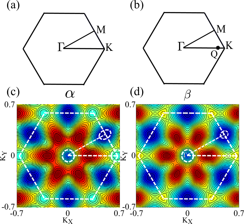
InTe has consisted of two In sub-layers is sandwiched between two Te sub-layers. For clarifying of valleys and high symmetry points, conduction band energy in the first Brillouin zone is plotted for and structures in Fig. 1. - and -valleys are indicated for both structures. Another valley is located at K-point for phase whereas, this valley takes some distance from K and is located at Q-point for phase (see Fig. 1). and valleys for phase and and valleys for phase show circular contour, whereas, an ellipsoidal contour is obvious for valley for both structures. An effective mass in the bottom of the conduction band is calculated for , and valleys. Whereas, two effective masses should be defined for valley with elliptical shape, longitudinal and transverse effective masses. High symmetry path to plot band structure is indicated for two phases, see Fig. 1.
III.1 Conduction Band Minimum
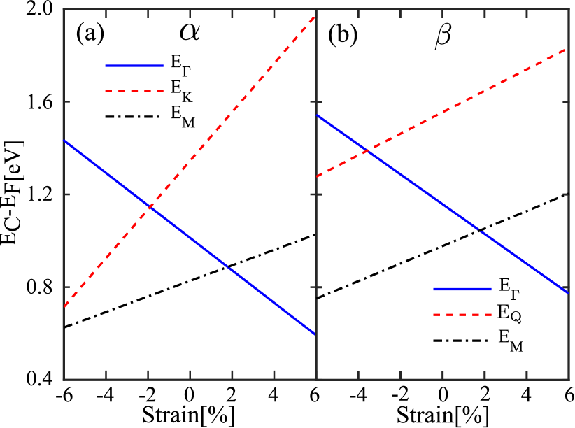
In Fig. 2, conduction, and valance bands are plotted along the high symmetry paths as is indicated in Fig. 1(a) and (b). The band structure is plotted for three strains- strain, unstrained and strain. For unstrained one, valley is lower than other valleys and located at the conduction band minimum (CBM). As one can see, the strain can modify shape and energy for each valley. For example, at phase with strain, both and valleys are closed to the CBM and contribute to electron transport. In this situation, effective mass for two valleys should be considered. At the other hand, valley is dominant for phase at strain. In unstrained one, CBM is located at valley for both structures. But in strain, both phases show CBM at the valley.

Strain from to is applied to both and phases and energies at the bottom of the valleys is plotted in Fig. 3. The energy in the bottom of two valleys ( and for phase and and for phase) increases respect to strain increasing, whereas, valley declines with increases of strain. As one can observe, the minimum energy of valleys change linear respect to strain and an equation is fitted to every curve. Relations between energy and strain form fitted equations are addressed in the following for two and phases.
| (2) | ||||
that is applying strain in percent. and stand for conduction band energies in and structures, respectively.
Electrons are located at the bottom of the conduction band and CBM highly affects electron transmission. For strains larger than , is the minimum conduction band and is the second minimum conduction band. For strain lower than , comes under other valleys so CBM moves to -valley. and phases behave similar, but -valley declines in phase more than it in phase in respect to strain. For strain , reaches close to . For both phases, band-gap goes to direct for tensile strain larger than . This suggests strained InTe is suitable for optical works at these strains.
III.2 Effective mass
Two valleys on and points, show circular valley that an effective masses are obtained but for the elliptical valley at point two longitudinal and transverse effective masses are calculated. In Fig. 4, effective mass of the valleys for and phases are calculated. In unstrained condition, we obtained effective mass for equal to 0.19 for phase, that approximately is close to 0.17 reported by Ref. [Zólyomi et al., 2014a]. They reported effective mass for -valley as 0.53 that here we obtained 0.47. The longitudinal and transverse effective masses of -valley are calculated as 0.52 and 0.29 that are close to reported effective masses Zólyomi et al. (2014a). These values for the structure are calculated. They reported 0.16 for valley of phase and we obtained 0.18 for it. They didn’t report any effective mass for -valley. We observed the valley is located at point near to point. The effective for this valley is obtained as 0.56. We calculate the longitudinal and transverse effective masses for -valley as 0.45 and 0.31.
The Fig. 4 shows that decreases when strain increasing. -valley shows the smallest effective mass for two phases at all range of strain. The effective mass of strained InTe is about 0.2 when CBM has located at -valley. In the opposite of -valley, effective mass at -valley for phase and -valley for phase increases with strain increasing. For strain larger than in phase, the valley at point vanishes and no effective mass is reported. For -valley, longitudinal effective mass increases with strain, whereas, transverse effective mass decreases.
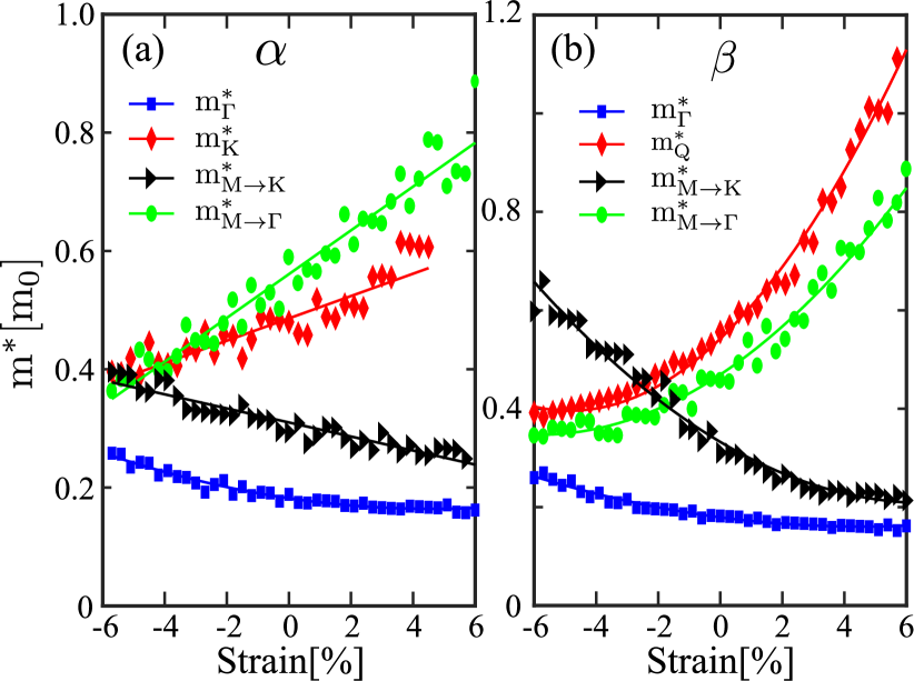
Effective masses for both phases smoothly vary with strain. Therefore, a line can be fitted to every effective mass curve. The fitted equations for phase at , , and respect with strain are listed in the following.
| (3) | ||||
In the following, equations for fitted line of effective mass respect to strain in phase are as:
| (4) | ||||
Effective mass at -valley for two phases show similar variation respect to strain. One can conclude two phases behave similarly when CBM is located at -valley.
III.3 FET results
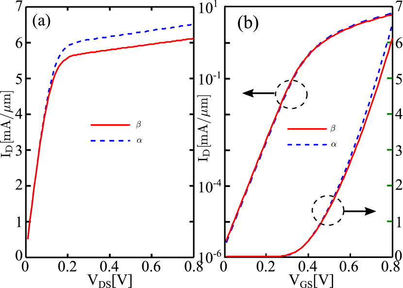
In this section, the electronic properties of strained InTe are studied. Mono-layer of InTe is used as a channel in a FET. Drain current is calculated by using the top of the barrier model. as a function of drain voltage for two phases is plotted in Fig. 5(a). increases with up to in linear regime then is saturated. Therefore, is enough to bring in the saturation regime. phase with lower effective mass shows higher current in the saturated regime.
as a function of gate voltage in linear and logarithmic scale is plotted in Fig. 5(b). increases exponentially with respect to the gate voltage in the sub-threshold regime and approximately are saturated for . Two phases behave similarly in logarithmic scale whereas phase indicates higher ON-current () in linear scale.
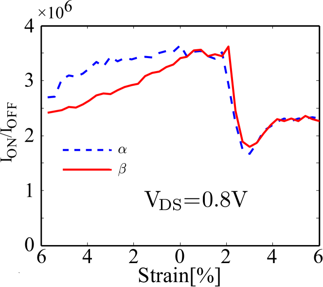
ION/IOFF ratio, an important parameter of a FET, is plotted as a function of strain for two phases in Fig. 6. This parameter stands larger than for all range of strain. ION/IOFF ratio increase respect to strain up to then falls down. CBM is located at M-valley for strain in the interval [-6,2] and goes to -valley for strain larger than . Changing CBM from M-valley to -valley causes ION/IOFF ratio falls down. Although, -valley shows less effective mass but six valleys for M-valley in the first Brillouin zone contribute to larger ON-current and larger ION/IOFF. For strain in the interval [-6,2], effective mass at M-valley decreases and ON-current increment causes ION/IOFF ratio increases. The results indicate that tensile strain decreases the performance of InTe FET. ION/IOFF ratio can decrease two times by tensile strain.
IV conclusions
Location of the valleys in the first Brillouin zone for mono-layer InTe is obtained. Three valleys at M, K(Q) and points for () phase contribute to electrical properties. The minimum energy of these valleys as a function of strain is calculated. It is observed CBM is located at -point for strain larger than whereas lies at -valley for smaller strain. Effective mass as a function of strain is calculated for these valleys and a curve is fitted to effective mass and minimum energy of each valley. -valley shows the lowest effective mass for all the range of strain. The results for FET simulation indicates an ION/IOFF ratio in the range and tensile strain decreases it until two times.
References
- Taur and Ning (2013) Y. Taur and T. H. Ning, Fundamentals of modern VLSI devices (Cambridge university press, 2013).
- Chaudhry and Kumar (2004) A. Chaudhry and M. J. Kumar, IEEE Trans. Device Mater. Reliab. 4, 99 (2004).
- Wang et al. (2012) Q. H. Wang, K. Kalantar-Zadeh, A. Kis, J. N. Coleman, and M. S. Strano, Nat. Nanotechnol. 7, 699 (2012).
- Wu et al. (2017) Y. Wu, D. Zhang, K. Lee, G. S. Duesberg, A. Syrlybekov, X. Liu, M. Abid, M. Abid, Y. Liu, L. Zhang, et al., Adv. Mater. Technol. 2, 1600197 (2017).
- Li et al. (2015) X.-B. Li, S.-Y. Xie, H. Zheng, W. Q. Tian, and H.-B. Sun, Nanoscale 7, 18863 (2015).
- Radisavljevic et al. (2011) B. Radisavljevic, A. Radenovic, J. Brivio, i. V. Giacometti, and A. Kis, Nat. Nanotechnol. 6, 147 (2011).
- Braga et al. (2012) D. Braga, I. Gutiérrez Lezama, H. Berger, and A. F. Morpurgo, Nano Lett. 12, 5218 (2012).
- Lei et al. (2014) S. Lei, L. Ge, S. Najmaei, A. George, R. Kappera, J. Lou, M. Chhowalla, H. Yamaguchi, G. Gupta, R. Vajtai, et al., ACS nano 8, 1263 (2014).
- Mudd et al. (2015) G. W. Mudd, S. A. Svatek, L. Hague, O. Makarovsky, Z. R. Kudrynskyi, C. J. Mellor, P. H. Beton, L. Eaves, K. S. Novoselov, Z. D. Kovalyuk, et al., Adv. Mater. 27, 3760 (2015).
- Mudd et al. (2013) G. W. Mudd, S. A. Svatek, T. Ren, A. Patanè, O. Makarovsky, L. Eaves, P. H. Beton, Z. D. Kovalyuk, G. V. Lashkarev, Z. R. Kudrynskyi, et al., Adv. Mater. 25, 5714 (2013).
- Late et al. (2012) D. J. Late, B. Liu, J. Luo, A. Yan, H. R. Matte, M. Grayson, C. Rao, and V. P. Dravid, Adv. Mater. 24, 3549 (2012).
- Schwarz et al. (2014) S. Schwarz, S. Dufferwiel, P. Walker, F. Withers, A. Trichet, M. Sich, F. Li, E. Chekhovich, D. Borisenko, N. N. Kolesnikov, et al., Nano Lett. 14, 7003 (2014).
- Feng et al. (2014) W. Feng, W. Zheng, W. Cao, and P. Hu, Advanced Materials 26, 6587 (2014).
- Bandurin et al. (2017) D. Bandurin, A. Tyurnina, G. Yu, A. Mishchenko, V. Zólyomi, S. Morozov, R. K. Kumar, R. Gorbachev, Z. Kudrynskyi, S. Pezzini, et al., Nat. Nanotechnol. 12, 223 (2017).
- Kuroda and Nishina (1980) N. Kuroda and Y. Nishina, Solid State Commun. 34, 481 (1980).
- Ho (2016) C.-H. Ho, 2D Mater. 3, 025019 (2016).
- Tamalampudi et al. (2014) S. R. Tamalampudi, Y.-Y. Lu, R. Kumar U, R. Sankar, C.-D. Liao, K. Moorthy B, C.-H. Cheng, F. C. Chou, and Y.-T. Chen, Nano Lett. 14, 2800 (2014).
- Sucharitakul et al. (2015) S. Sucharitakul, N. J. Goble, U. R. Kumar, R. Sankar, Z. A. Bogorad, F.-C. Chou, Y.-T. Chen, and X. P. Gao, Nano Lett. 15, 3815 (2015).
- Feng et al. (2015) W. Feng, X. Zhou, W. Q. Tian, W. Zheng, and P. Hu, Phys. Chem. Chem. Phys. 17, 3653 (2015).
- Sánchez-Royo et al. (2014) J. F. Sánchez-Royo, G. Muñoz-Matutano, M. Brotons-Gisbert, J. P. Martínez-Pastor, A. Segura, A. Cantarero, R. Mata, J. Canet-Ferrer, G. Tobias, E. Canadell, et al., Nano Res. 7, 1556 (2014).
- Zólyomi et al. (2014a) V. Zólyomi, N. Drummond, and V. Fal’Ko, Phys. Rev. B 89, 205416 (2014a).
- Demirci et al. (2017) S. Demirci, N. Avazlı, E. Durgun, and S. Cahangirov, Phys. Rev. B 95, 115409 (2017).
- Zólyomi et al. (2014b) V. Zólyomi, N. Drummond, and V. Fal’Ko, Phys. Rev. B 89, 205416 (2014b).
- Yu et al. (2015) S. Yu, H. D. Xiong, K. Eshun, H. Yuan, and Q. Li, Appl. Surf. Sci. 325, 27 (2015).
- Jalilian and Safari (2017) J. Jalilian and M. Safari, Phys. Lett. A 381, 1313 (2017).
- Ariapour and Touski (2019) M. Ariapour and S. B. Touski, Mater. Res. Express 6, 076402 (2019).
- Giannozzi et al. (2009) P. Giannozzi, S. Baroni, N. Bonini, M. Calandra, R. Car, C. Cavazzoni, D. Ceresoli, G. L. Chiarotti, M. Cococcioni, I. Dabo, et al., J. Phys.:Condens. Matter 21, 395502 (2009).
- Giannozzi et al. (2017) P. Giannozzi, O. Andreussi, T. Brumme, O. Bunau, M. B. Nardelli, M. Calandra, R. Car, C. Cavazzoni, D. Ceresoli, M. Cococcioni, et al., J. Phys.:Condens. Matter 29, 465901 (2017).
- Perdew et al. (2008) J. P. Perdew, A. Ruzsinszky, G. I. Csonka, O. A. Vydrov, G. E. Scuseria, L. A. Constantin, X. Zhou, and K. Burke, 100, 136406 (2008).