Experimental generation of phase wraps for subwavelength phase structures in Bose-Einstein condensate with two-dimensional optical lattice
Abstract
We report an experimental demonstration of engineering phase wraps for sub-wavelength structure in a Bose-Einstein condensate (BEC) with two-dimensional optical lattices. A short lattice pulse is applied on BEC working in the Kapitza-Dirac (or Raman-Nath) regime, which corresponds to phase modulation imprint on matter wave. When the phase modulation on matter wave is larger than in a lattice cell, there appears phase wraps with multiple jumps, generating the sub-wavelength phase structure. The phase wraps for sub-wavelength structure are measured in momentum space via the time-of-flight absorption image, which corresponds to converting phase information into amplitude. Moreover, we identify an additional condition for the validity of Kapitza-Dirac regime, which relies crucially on the lattice configurations. This scheme can be used for studying the property of optical lattices and topological defects in matter wave.
The resolution of a conventional optical system is limited by the wavelength of light waves due to diffraction Rayleigh ; Born . For a standing wave created by two laser fields with wavelength , the lattice spacing between adjacent intensity maxima is , where , with being the intersecting angle between the two fields. Therefore, the spatial resolution of interferometric lithography is always limited to Brueck1998 . Circumventing this limit to create pattens with spatial resolution smaller than is not only interesting for a fundamental point of view, but also relevant for the semiconductor industry. In the past decades, many schemes have been proposed to improve the spatial resolution of interferometric lithography beyond the diffraction limit, including the schemes of multiphoton nonlinear processes with classical lights Bentley2004 ; Avi2004 ; Hemmer2006 , quantum lithography with quantum entanglement Dowling2000 ; Kok2001 ; Agarwal2001 ; D'Angelo2001 , quantum dark state Agarwal2006 ; Kiffner2008 ; Li2008 , Rabi oscillations Liao2010 ; Rui2016 , coherent atom lithography Liao2013 ; Fouda2016 .
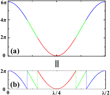
In this paper, we experimentally develop and demonstrate a new scheme that generate sub-wavelength structure using the idea of phase wrap. In literature, the phase wrapping and unwrapping problems Itoh1982 have a variety of applications, such as terrain elevation estimation in synthetic aperture radar Jakowatz2016 , field mapping in magnetic resonance imaging Fouda1991 , wavefront distortion measurement in adaptive optics Fried1997 , and is also concerned with topological defects and singularities Ghiglia1998 . The idea of phase wrap in our work is implemented in a Bose-Einstein condensate (BEC) by applying two-dimensional (2D) optical lattices. A short pulse of optical lattice is illuminated on BEC working in the regime of Kapitza-Dirac (or Raman-Nath) scattering. In this process, the lattice potential imprints a phase modulation on matter wave in spatial space, as shown schematically in Fig. 1. When the phase modulation on matter wave is larger than within a lattice cell, as shown in Fig. 1(a), the continuous phase curve can be equivalent to the phase wrap curve as multiple jumps forming a saw-tooth waveform in the principal value range of , as shown in Fig. 1(b). In this case, the phase wrap curve form the sub-wavelength phase structure, and the wrapping number gives the sub-wavelength . We measure sub-wavelength phase structure in momentum space via the time-of-flight absorption image, which corresponds to converting phase information into amplitude. Here, we work with two different kinds of 2D optical lattices, and the sub-wavelength phase patterns show the properties of the optical lattice.
Now we discuss how the optical lattice pulse imprints a phase modulation on matter wave. Here we apply a short pulse of optical lattice on BEC working in the Kapitza-Dirac regime Gould1986 ; Ovchinnikov1999 ; Oberthaler1999 ; Gadway2009 limited to pulse duration , where is the photon recoil energy. Previous studies have shown that under a pulse that is short enough, the kinetic energy can be neglected, thus the lattice potential simply acts as a phase grating on the matter wave Oberthaler1999 . In this work, we show that besides the short lattice pulse, the phase grating on matter wave (or the neglecting of kinetic energy) requires an additional condition on the configuration of lattice potentials. Under such condition, the Kapitza-Dirac regime is equivalent to that the effect of short lattice pulse is to impose a spatially periodic phase modulation on the matter wave.
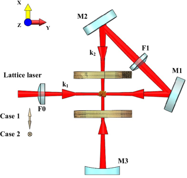
In our experiment, the ultracold 87Rb atoms in the state is prepared in the crossed optical dipole trap Xiong2010 . Here denotes the total angular momentum and the magnetic quantum number of the state. Forced evaporation in the optical trap is used to create the BEC with up to atoms, which is used as the coherent matter wave. The lattice beam is derived from a single frequency Ti:sapphire laser and operated at a wavelength of nm. An acousto-optical modulator is used to control the intensity of the lattice beam. Then the light is coupled into a polarization maintaining fiber to provide a clean spatial mode. A polarizer after the fiber creates a well defined polarization in the x-z plane. In order to generate two different kinds of 2D optical lattice potentials, we employ the scheme of folded retroreflected mirrors, as shown in Fig. 2. This scheme has been used to experimentally design and implement the 2D optical lattice of double wells suitable for isolating and manipulating an array of individual pairs of atoms Strabley2006 and predict a topological semimetal in the high orbital bands in this 2D lattice Sun2012 . The light is folded by plane mirrors M1 and M2 and then retroreflected by concave mirror M3. Therefore, the incoming beam with wave vector is reflected by mirrors M1 and M2 and refocus on the atomic cloud with wave vector , and two wave vectors intersect orthogonally. Lenses F0 and F1 with the concave mirror M3 generate almost the same focus beam radius at the intersection of the four beams with the radius of 200 m.
We first consider the case 1 when the linear polarization of incident laser beam is aligned parallel to the drawing plane (referred as in-plane lattice). Due to the orthogonal intersection of laser beam and the orthogonality of the polarization between and , the resulting 2D lattice is a square lattice formed by two independent 1D lattices. The potential of 2D square lattice is described by
| (1) |
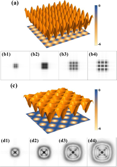
Here and denotes the wavelength of the lattice beam. This generates a 2D square lattice with antinode (nodes) spaced by along x and y respectively, as shown in Fig. 3(a).
As the case 2, the linear polarization of incident laser beam is aligned normal to the drawing plane (referred as out-plane lattice). In this case the potential is not simply a sum of independent lattices in x and y, but rather given by
| (2) |
The extra interference term, in Eq. 2, induces the lattice period with along and directions. When the lattice laser is red detuning (), the generated lattice is just like to dug the holes on the ground and there are nodal lines along the diagonals as shown in Fig. 3(c). Different from the square lattice in Eq. 1, here the out-plane lattice in Eq. 2 displays different shapes near the antinode and node. We will show later that this property would significantly affect the sub-wavelength structure as measured in our experiment.
As discussed previously, when work in the Kapitza-Dirac regime and neglect the kinetic energy of matter wave, the evolution of BEC after a short pulse duration can be described classically by
| (3) |
Here is the Gaussian wave function of initial state of BEC, while the lattice potential imprints a phase modulation on the BEC. Take the in-plane lattice for example, when the phase of BEC within a unit cell appears as multiple jumps, known as phase wraps. Similarly, the phase wrap occurs for out-plane lattice when . Such phase wraps equivalently generate the sub-wavelength structure, as schematically shown in Fig. 1, where the wrapping number gives the sub-wavelength . Since we can not directly measure the phase structure of BEC by the in-situ imaging, we must convert the phase information into amplitude. The easiest way to realize this goal is to take the Fourier transform
| (4) |
This transformation converts the phase information of real-space wave function to the amplitude information in momentum space. The resulted intensity distribution in momentum space can be directly measured in the ultracold atomic experiment through the time-of-flight absorption image.
In Figs. 3(b1)-(b4) and (d1)-(d4), we show the intensity distributions from Eqs. 3 and 4 corresponding to the two different lattice potentials as displayed, respectively, in Fig. 3(a) and (c). Starting with the initial BEC which has a single momentum component (), the phase modulations with the 2D optical lattices generate discrete momentum components. Remarkably, these discrete components organize themselves into different pattens in a larger momentum scale, which is related to phase wraps in a smaller length scale (within a single cell), leading to the sub-wavelength structure. Since the in-plane lattice generates the sub-wavelength phase structure with the trenches along x and y (Fig. 3(a)), the intensity distribution after the Fourier transform presents the larger line structures along x and y, see Fig. 3(b1)-(b4). In contrast, out-plane lattice generates the sub-wavelength phase structure with ring structure (Fig. 3(c)) and the intensity distribution after the Fourier transform presents the larger ring structures, see Fig. 3(d1)-(d4).
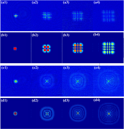
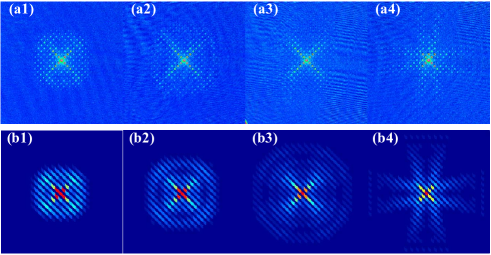
In the experiment, for the lattice wavelength of nm, which is red detuning corresponding to in Eqs. 1 and 2 . We apply 2D optical lattice short pulse with 4 on BEC, which work in the Kapitza-Dirac regime. Then we immediately turn off the optical trap, let the atoms ballistically expand in 7 ms and take the absorption image. Fig. 4(a1)-(a4) show the atomic density distribution of the time-of-flight absorption image after applying in-plane lattice pulse on BEC and Fig. 4(c1)-(c4) are for out-plane lattice. These experimental data are in good consistence with theoretical results from the full quantum evolution of the BEC (see supplementary material), as shown by Figs. 4(b1)-(b4) and 4(d1)-(d4). The results are also qualitatively consistent with those from the classical treatment (Eq. 3) (see supplementary material sup ).
As expected, the atomic density distributions of the time-of-flight absorption image exhibit discrete momentum components. Nevertheless, the distribution of the discrete momentum components is not uniform, which depends on the sub-wavelength phase structure in a lattice cell. In a larger momentum scale, the distribution of discrete momentum components shows line structure along x and y for in-plane lattice, and ring structure for out-plane lattice. As increasing the lattice laser power, more and more lines or rings appear, see Fig. 4. This can be well explained by the phase wrap picture since more and more phase jumps occurs within the single cell as increasing , giving more delicate structure with smaller sub-wavelength. In this way, the line or ring pattens in a large momentum scale of the intensity distribution directly reflect the sub-wavelength structure of particular lattice potentials.
To this end, we have shown the validity of classical treatment (Eq. 3) in predicting the BEC dynamics, which neglects the quantum motion of the wave-packet due to the kinetic term. Nevertheless, it is noted that the classical treatment does not only reply on the short lattice pulse, but also require an additional condition on the configuration of lattice potentials. In above experiments, we consider lattice potentials and in Eqs. 1 and 2 exhibiting sharp structure near the bottom, as seen from Fig. 3(a) and (c). In this case, the low-energy states, which have the largest overlap with the initial BEC wave-packet and contribute most to the BEC dynamics, are well localized and thus able to reflect the structure of lattice potentials. As a result, the phase modulation formula (Eq. 3) can be a good approximation to mimic the BEC dynamics. To summarize, this additional condition is that the lattice supported low-energy states are sufficiently localized, such that the quantum motion of BEC can be efficiently suppressed to allow the neglecting of kinetic energy.
To further demonstrate this additional condition, we have performed an additional set of experiments with the out-of-plane lattice pulse switching to blue detuning, i.e., with in Eq. 2. In this case, the bottom of the lattice potential is fairly smooth and the quantum motion of low-energy states can not be neglected, which does not satisfy the additional condition of neglecting the kinetic energy. The phase modulation formula Eq. 3 is not applicable any more. Experimentally, no clear ring structure can be found in large limit, see Fig. 5, in contrast to the red detuning case with large . The observation is consistent with results from the full quantum calculation but not with the classical treatment, see supplementary material sup .
In conclusion, we have experimentally observed the phase wraps for sub-wavelength structure in BEC with two-dimensional optical lattices. The phase wraps are realized by applying a short lattice pulse in the Kapitza-Dirac regime, such that the lattice potentials imprint the phase modulation on matter wave. We have detected this sub-wavelength phase structure in a lattice cell by measuring the intensity distribution of BEC in momentum space, which shows the line or ring structures in a larger momentum scale. Furthermore, we have demonstrated an additional condition for the application of the Kapitza-Dirac regime where the kinetic energy can be neglected. The result can be used to detect more properties of the optical lattice, such as the shape of the lattice cell and the localized property of low-energy Bloch states. Finally, the phase wrapping picture in our work can also be connected to the topological defects in matter wave, such as phase steps or vortices.
‡Corresponding author email: jzhang74@sxu.edu.cn, jzhang74@yahoo.com.
Acknowledgements.
This research is supported by the National Key Research and Development Program of China (2016YFA0301602, 2018YFA0307600, 2016YFA0300603), NSFC (Grant No. 11234008, 11474188, 11704234, No.11622436, No.11421092, No.11534014) and the Fund for Shanxi ”1331 Project” Key Subjects Construction.References
- (1) L. Rayleigh, XXXI. Investigations in optics, with special reference to the spectroscope, Philos. Mag. 8, 261 (1879).
- (2) M. Born and E. Wolf, Principles of optics: electromagnetic theory of propagation, interference and diffraction of light (New York: Pergamon Press, 1980), 6th edn.
- (3) S. R. J. Brueck, S. H. Zaidi, X. Chen, and Z. Zhang, Interferometric lithography-from periodic arrays to arbitrary patterns, Microelectron. Eng. 41/42, 145 (1998).
- (4) S. J. Bentley and R. W. Boyd, Nonlinear optical lithography with ultra-high sub-Rayleigh resolution, Opt. Express 12, 5735 (2004).
- (5) A. Pe’er, B. Dayan, M. Vucelja, Y. Silberberg, and A. A. Friesem, Quantum lithography by coherent control of classical light pulses, Opt. Express 12, 6600 (2004).
- (6) P. R. Hemmer, A. Muthukrishnan, M. O. Scully, and M. S. Zubairy, Quantum lithography with classical light, Phys. Rev. Lett. 96, 163603 (2006).
- (7) A. N. Boto, P. Kok, D. S. Abrams, S. L. Braunstein, C. P. Williams, and J. P. Dowling, Quantum interferometric optical lithography: Exploiting entanglement to beat the diffraction limit, Phys. Rev. Lett. 85, 2733 (2000).
- (8) P. Kok, A. N. Boto, D. S. Abrams, C. P. Williams, S. L. Braunstein, and J. P. Dowling, Quantum-interferometric optical lithography: Towards arbitrary two-dimensional patterns, Phys. Rev. A 63, 063407 (2001).
- (9) G. S. Agarwal, R. W. Boyd, E. M. Nagasako, and S. J. Bentley, Comment on ”Quantum interferometric optical lithography: Exploiting entanglement to beat the diffraction limit”, Phys. Rev. Lett. 86, 1389 (2001).
- (10) M. D’Angelo, M. V. Chekhova, and Y. Shih, Two-photon diffraction and quantum lithography, Phys. Rev. Lett. 87, 013602 (2001).
- (11) G. S. Agarwal and K. T. Kapale, Subwavelength atom localization via coherent population trapping, J. Phys. B: At. Mol. Opt. Phys. 39, 3437 (2006).
- (12) M. Kiffner, J. Evers, and M. S. Zubairy, Resonant interferometric lithography beyond the diffraction limit, Phys. Rev. Lett. 100, 073602 (2008).
- (13) H. Li, V. A. Sautenkov, M. M. Kash, A. V. Sokolov, G. R. Welch, Y. V. Rostovtsev, M. S. Zubairy, and M. O. Scully, Optical imaging beyond the diffraction limit via dark states, Phys. Rev. A 78, 013803 (2008).
- (14) Z. Liao, M. Al-Amri, and M. Suhail Zubairy, Quantum lithography beyond the diffraction limit via Rabi oscillations, Phys. Rev. Lett. 105, 183601 (2010).
- (15) J. Rui, Y. Jiang, G. Lu, M. Zhu, B. Zhao, X. Bao, and J. Pan, Demonstration of interferometric atom-pattern engineering via Rabi oscillations, Phys. Rev. A 93, 033837 (2016).
- (16) Z. Liao, M. Al-Amri, T. Becker, W. P. Schleich, M. O. Scully, and M. S. Zubairy, Atom lithography with subwavelength resolution via Rabi oscillations, Phys. Rev. A 87, 023405 (2013).
- (17) M. F. Fouda, R. Fang, J. B. Ketterson, and M. S. Shahriar, Generation of arbitrary lithographic patterns using Bose-Einstein-condensate interferometry, Phys. Rev. A 94, 063644 (2016).
- (18) K. Itoh, Analysis of the phase unwrapping algorithm, Appl. Opt. 21, 2470 (1982).
- (19) C. V. Jakowatz, Jr., D. E. Wahl, P. H. Eichel, D. C. Ghiglia, and P. A. Thompson, Spotlight-mode synthetic aperture radar: A signal processing approach (Boston: Springer, 1996), 1th edn.
- (20) G. H. Glover and E. Schneider, Three-point dixon technique for true water/fat decomposition with B0 inhomogeneity correction, Magn. Reson. Med. 18, 371 (1991).
- (21) D. L. Fried, Least-square fitting a wave-front distortion estimate to an array of phase-difference measurements, J. Opt. Soc. Am. 67, 370 (1977).
- (22) D. C. Ghiglia and M. D. Pritt, Two-dimensional phase unwrapping: Theory, algorithms, and software (New York: John Wiley Sons, 1998), 1th edn.
- (23) P. L. Gould, G. A. Ruff, and D. E. Pritchard, Diffraction of atoms by light: The near-resonant Kapitza-Dirac effect, Phys. Rev. Lett. 56, 827 (1986).
- (24) Y. B. Ovchinnikov, J. H. Mller, M. R. Doery, E. J. D. Vredenbregt, K. Helmerson, S. L. Rolston, and W. D. Phillips, Diffraction of a released Bose-Einstein condensate by a pulsed standing light wave, Phys. Rev. Lett. 83, 284 (1999).
- (25) M. K. Oberthaler, R. M. Godun, M. B. d’Arcy, G. S. Summy, and K. Burnett, Observation of quantum accelerator modes, Phys. Rev. Lett. 83, 4447 (1999).
- (26) B. Gadway, D. Pertot, R. Reimann, M. G. Cohen, and D. Schneble, Analysis of Kapitza-Dirac diffraction patterns beyond the Raman-Nath regime, Opt. Express 17, 19173 (2009).
- (27) D. Xiong, P. Wang, Z. Fu, S. Chai, and J. Zhang, Evaporative cooling of 87Rb atoms into Bose-Einstein condensate in an optical dipole trap, Chin. Opt. Lett. 8, 627 (2010).
- (28) J. Sebby-Strabley, M. Anderlini, P. S. Jessen, and J. V. Porto, Lattice of double wells for manipulating pairs of cold atoms, Phys. Rev. A 73, 033605 (2006).
- (29) K. Sun, W. V. Liu, A. Hemmerich, and S. Das Sarma, Topological semimetal in a fermionic optical lattice, Nat. Phys. 8, 67 (2012).
- (30) See Supplementary Material for more details about the full quantum calculation and the comparision with classical treatment.