Nano-mosaic of Topological Dirac States on the Surface of Pb5Bi24Se41 Observed by Nano-ARPES
Abstract
We have performed scanning angle-resolved photoemission spectroscopy with a nanometer-sized beam spot (nano-ARPES) on the cleaved surface of Pb5Bi24Se41, which is a member of the (PbSe)5(Bi2Se3)3m homologous series (PSBS) with = 4 consisting of alternate stacking of the topologically-trivial insulator PbSe bilayer and four quintuple layers (QLs) of the topological insulator Bi2Se3. This allows us to visualize a mosaic of topological Dirac states at a nanometer scale coming from the variable thickness of the Bi2Se3 nano-islands (1-3 QLs) that remain on top of the PbSe layer after cleaving the PSBS crystal, because the local band structure of topological origin changes drastically with the thickness of the Bi2Se3 nano-islands. A comparison of the local band structure with that in ultrathin Bi2Se3 films on Si(111) gives us further insights into the nature of the observed topological states. This result demonstrates that nano-ARPES is a very useful tool for characterizing topological heterostructures.
Three-dimensional topological insulators (TIs) are a novel quantum state of matter where gapless surface states (SSs) emerge inside the bulk band gap inverted by a strong spin-orbit coupling.1 ; 2 ; 3 Topological SSs are characterized by a Dirac-cone energy dispersion with a helical spin texture and play an essential role in realizing exotic quantum phenomena. The discovery of TIs has also stimulated the exploration of new topological materials beyond TIs such as topological semimetals hosting Dirac/Weyl fermions in the bulk band structure4 and topological superconductors with Majorana fermions.5 ; 6 While bulk crystals and thin films have been the main platforms for investigating topological properties/phenomena so far, multilayer heterostructures (superlattices) consisting of alternately-stacked two or more different materials are now attracting much attention as a promising platform.7 ; 8 ; 9 ; 10 ; 11 ; 12 ; 13 ; 14 ; 15 ; 16 ; 17 ; 18 ; 19 ; 20 ; 21 ; 22
In heterostructures, one can control the thickness and stacking sequence of layers and/or insert different building blocks to modulate physical parameters (e.g., spin-orbit coupling, hybridization effect, and crystal symmetry) and obtain ordered phases (magnetism and superconductivity). This wide tunability in heterostructures is a great advantage to realize novel topological phases and gigantic quantum effects absent in parent materials. For example, for a heterostructure of TI and nontopological material where each TI interface hosts topologically-protected states (interface states; ISs), it has been proposed that precise control of the hybridization strength between adjacent ISs and/or the coupling between ISs and a certain order in the building block would lead to various novel phenomena. This is highlighted by a topological phase transition in a heterostructure of TI and nontopological insulator (NI),9 a magnetic Weyl semimetal phase in a magnetically-doped TI/NI heterostructure,7 and a Weyl superconductor phase in a magnetically-doped TI/superconductor heterostructure.8
Since such novel properties of topological heterostructures are governed by the bulk electronic states and topological ISs/SSs that are strongly modified by the thickness, stacking sequence, or combination of building blocks, a systematic experimental determination of electronic states in each building block as a function of structural parameters is of particular importance to advance the exploration of exotic phenomena in topological heterostructures. It would thus be useful to utilize angle-resolved photoemission spectroscopy (ARPES) to directly observe the momentum-resolved band structure. However, ARPES study of topological heterostructures is rather scarce, partly because of the presence of multiple domains that usually appear on the surface. Since the size of such domains is typically much smaller than the beam spot of conventional ARPES apparatus ( 100 m), it is very hard to obtain ARPES data by specifying each building block. To overcome such a problem, it is of particular importance to uncover the complexity of the electronic structure characterized by the entanglement of IS, SS and bulk electronic bands not only by high energy and momentum resolution but also by lateral resolution in the real space, in the scale of the nanometer.
In this Letter, we report the first nano-ARPES study of a topological heterostructure. The material is Pb5Bi24Se41, a new member of naturally-occurring bulk TI/NI heterostructure (PbSe)5(Bi2Se3)3m (called PSBS) with = 4,23 ; 24 ; 25 ; 26 which consists of alternately-stacked four quintuple layers (QLs) of TI (Bi2Se3) and one bilayer of NI (PbSe) (see Figure 1a). By utilizing a very small beam spot of 120 nm with a piezo-based sample positioning system, we have directly visualized a marked spatial variation of the valence-band structure and core-level states in PSBS and determined the size, shape, and distribution of different domain structures. Remarkably, selective probing of each domain revealed the evolution of the bulk bands and topological ISs/SSs as a function of the thickness of Bi2Se3 layers on a single sample. The present study not only provides important insight into the topological property of PSBS but also demonstrates the great advantage of nano-ARPES for investigating the electronic states of topological heterostructures.
High-quality single crystal of PSBS ( = 4) was grown by a combination of modified Bridgman and self-flux methods using high purity elements (Pb 99.998%, Bi and Se 99.9999%) in a sealed evacuated quartz tube.23 Ultrathin films of Bi2Se3, used as a reference, were grown on Si(111) by the molecular-beam-epitaxy (MBE) method. The film thickness was controlled by the deposition time at a constant deposition rate. The actual thickness was determined by the oscillation pattern of reflection high-energy electron diffraction (RHEED). ARPES measurements for PSBS were performed with a MBS-A1 electron analyzer with energy-tunable synchrotron light at the ANTARES beamline in SOLEIL and with a Scienta-Omicron SES2002 spectrometer at the BL28A in Photon Factory (PF), KEK. We used circularly polarized light of 100 eV in SOLEIL and 40-80 eV in PF. Nano-ARPES measurements in SOLEIL were performed with submicron beam spot achieved by a Fresnel-zone-plate focusing system combined with a precise sample scanning system, optimized for an energy photon flux of 100 eV.27 ; 28 PSBS crystals were cleaved in-situ in an ultrahigh vacuum better than 110-10 Torr along the (111) crystal plane. ARPES measurements for Bi2Se3 thin films were carried out with an ARPES-MBE combined system at Tohoku University equipped with a MBS-A1 electron analyzer. We used the He-I ( = 21.218 eV) line to excite photoelectrons. PSBS crystals and Bi2Se3 thin films were kept at = 60 K in SOLEIL and 30 K in Tohoku University during ARPES measurements.
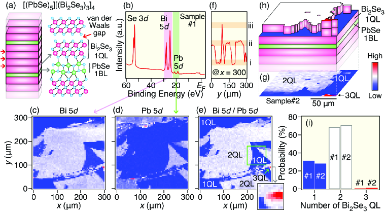
First, we performed a scanning core-level photoemission microscopy on PSBS () surface with a nano-focused beam. A representative energy-distribution curve (EDC) at a fixed sample position (Figure 1b) shows several shallow core levels of Se , Bi , and Pb . Figures 1c,d display real-space maps of Bi- and Pb- core-level intensities, respectively, measured on an area of m2. One can recognize a mosaic-like pattern that mainly consists of blue- and white-colored regions separated by a sharp boundary, indicative of formation of multiple domain structures on the cleaved surface. Their spatial distribution is random and the area of each domain varies from 200200 m2 to 55 m2, the latter of which is too small to resolve by conventional ARPES with a beam spot of 100 m. It is also noted that blue-colored (white-colored) domain in Figure 1c shows white (blue) color in Figure 1d. Because of this anticorrelation between the Bi- and Pb- core-level intensities, an enhanced color contrast is obtained by taking their relative intensity (see Figure 1e). In Figure 1e, besides blue- and white-colored domains, a small but finite red-colored domain (47-m2 area) is observed at (, ) (300 m, 100 m) (indicated by a green arrow), as can be seen more clearly in a fine map of 1010-m2 area which includes the red-colored region (see right bottom panel of Figure 1e). The existence of three types of domains is confirmed by a line profile at m (see Figure 1f) where the Bi-/Pb- intensity falls into three levels i-iii that correspond to blue-, white-, and red-colored domains in Figure 1e, respectively, and is further corroborated by the observation of a tricolor spatial image on a different sample surface (Figure 1g). The three-domain nature of PSBS ( = 4) surface is naturally understood in terms of three different cleavage planes in the crystal. Namely, the cleavage may preferably occur at each van der Waals gap between QLs within the Bi2Se3 unit (red arrows in Figure 1a), leaving 1-3 QLs of Bi2Se3 nano-islands on the PbSe layer. Specifically, blue-, white-, and red-colored regions in Figures 1e,g would correspond to 1-, 2-, and 3-QL Bi2Se3 islands, respectively (see schematic in Figure 1h), because the finite photoelectron escape depth leads to the stronger Bi-/Pb- intensity ratio for thicker Bi2Se3 domains. It is noted that the PbSe layer and the neighboring Bi2Se3 QL are connected with each other via Pb-Se bonds29 (see Figure 1a), so that cleavage between these two layers would rarely occur in PSBS, except for small phases (e.g., = 1). Our atomic-force microscopy measurements on PSBS with = 4 revealed a step structure with 1-nm height that is close to the thickness of 1-QL Bi2Se3, supporting the preferable cleavage between Bi2Se3 QLs (see Figure S1 in Supporting Information). Figure 1i displays the probability to observe each domain, estimated from the maps in Figures 1e,g (sample #1 and #2, respectively). A low probability (1-3 %) for seeing the 3-QL domain (also see Figures 1e,g) highlights the crucial importance of a real-space imaging with nano-focused beam spot to resolve all three domains. It is noted that the multiple domain structure was overlooked in a previous ARPES study on PSBS ( = 1 and 2) with a large beam spot.14
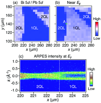
The selective observation of 1-3 QLs of Bi2Se3 islands by nano-ARPES provides an excellent opportunity to simultaneously investigate the band structure of Bi2Se3 with various thicknesses in one sample. Figures 2a,b display a comparison between the spatially resolved core-level and near- intensities measured in the same region of cleaved surface (green square in Figure 1e). One can identify similar mosaic pattern with reversed contrast between Figures 2a and 2b, such as a vertical domain boundary at 220 m and a diagonal domain boundary at upper right. This indicates a modification of the local band structure depending on the number of QLs. By using momentum-resolving capability of nano-ARPES, we further visualized the evolution of Fermi surface across the boundary between the 1-QL and 2-QL domains (along a cut A in Figure 2b). The ARPES intensity at as a function of and (Figure 2c) shows the presence of a single Fermi surface with the Fermi wave vector of 0.2 in the 1-QL domain, and a sudden change in the Fermi vector by passing through the domain boundary into the 2-QL domain, as represented by appearance of strong intensity at 0.1 . The observed domain-dependent near- intensity and Fermi surface are related to the in-plane mosaic of topological SSs/ISs as discussed later.
To gain further insight into the local band structure of Bi2Se3 nano-islands, we have performed high energy- and momentum-resolution ARPES measurements on each domain. In Figure 3a, a single parabolic band is observed for the 1-QL domain, consistent with a single Fermi surface observed in Figure 2c. On the other hand, multiple bands are resolved for the 2-QL domain, and the number of bands is further increased in the 3-QL domain. The observed domain-dependent change in the local band structure would be mainly triggered by quantum confinement within the Bi2Se3 layer.14 To understand the origin of the band dispersions in each domain, it is useful to compare the present ARPES results with those for ultrathin Bi2Se3 films, in which the band structure is strongly reconstructed by the electron confinement effect.30 As seen from Figure 3b, the overall band structure of Bi2Se3 ultrathin films on Si(111) substrate (Bi2Se3/Si) resembles that of PSBS. For example, 1-QL Bi2Se3/Si has a single parabola as in the 1-QL domain of PSBS, and 2-QL Bi2Se3/Si has a bandgap at 0.6 eV with a “M”-shaped dispersion of the lower hole-like branch as in the 2-QL domain of PSBS. This similarity strongly suggests that a parabolic band at the point in the 1-QL domain of PSBS (black dots in left panel of Figure 3a) is ascribed to the quantized bulk conduction band (CB), as is the case of Bi2Se3/Si.30 Also, for the 2-QL domain, two inner electron pockets (black dots) are quantized bulk CBs with a Rashba-type splitting, while two outer electron pockets and hole-like dispersions at higher ’s (red dots) are the upper and lower branches of gapped Dirac cones that originate from the hybridized topological SSs/ISs (note that the Rashba splittings of CB and hybridized topological SSs/ISs are a consequence of the inversion-symmetry breaking at the surface as observed in Bi2Se3/graphene30 ). Upon increasing the film thickness to 3 QL, the bulk valence band (VB) is well isolated from the lower Dirac band (see black dots at 0.7 eV in right panel of Figure 3b), accompanied by a reduction of hybridization gap at the Dirac point (see red dots). By taking into account these trends, the energy bands that produce the minimum band gap in the 3-QL domain of PSBS (red dots in right panel of Figure 3a) are assigned to the hybridized topological SSs/ISs, while other bands (black dots) are attributed to the quantized bulk bands; i.e., electron-like bands near and hole-like bands at higher ’s are the quantum well states of CB and VB, respectively.
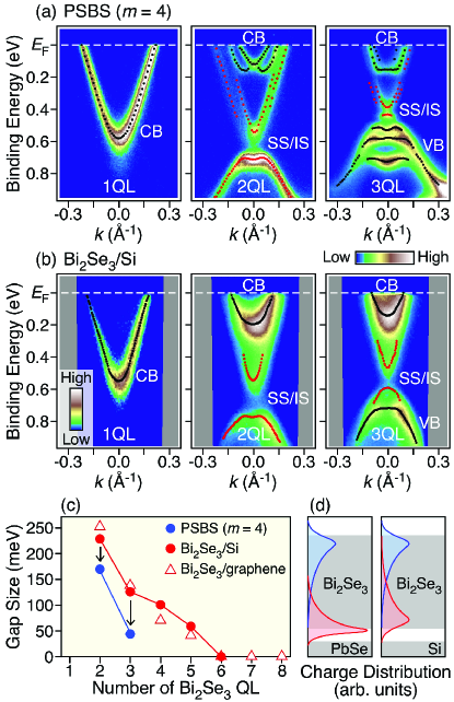
The present systematic investigation of the near- electronic states by domain-selective nano-ARPES allows us to discuss the evolution of topological properties as a function of the Bi2Se3 thickness (1-3 QLs). As seen in Figure 3a, while an inverted band structure in the 2- and 3-QL domains of PSBS leads to the appearance of topological SSs and ISs, their mutual hybridization results in gap-opening at the Dirac point. The observed hybridization-gap size is 170 meV and 40 meV for the 2- and 3-QL domains, respectively. Intriguingly, these values (see blue circles in Figure 3c) are substantially smaller than those for ultrathin Bi2Se3 films on various substrates such as Bi2Se3/Si and Bi2Se3/graphene30 (red circles and triangles, respectively). For example, the hybridization gap in the 3-QL domain of PSBS is as small as that in 5-QL Bi2Se3/Si and Bi2Se3/graphene. This suggests that the critical thickness of Bi2Se3 layer at which a gapless topological phase emerges in PSBS would be smaller than 6 QL that has been proposed for Bi2Se3 films.30 Possibly, the gapless topological phase may be realized in bulk PSBS with = 4. Such robustness of the topological phase down to ultrathin regime may be potentially useful for realizations of gigantic topological effects in bulk crystals as well as for future application to nano-scale devices. It is noted that high-resolution ARPES measurements on a different sample confirmed that the observed small hybridization gap is an intrinsic property of PSBS (see Figure S2 in Supporting Information).
The origin of the small hybridization gap in PSBS may be ascribed to a difference in the spatial distribution of topological ISs between PSBS and Bi2Se3/Si. It has been predicted for TI/NI heterostructures that the interaction with an interfaced NI may strongly modify the real-space distribution of topological ISs; for instance, topological ISs may migrate from TI to interfaced NI.9 Therefore, one may expect that the wave function of topological ISs is localized at the interface or even shifted toward the PbSe layer compared with that in Bi2Se3/Si (see red shades in the schematics of Figure 3d) and the resultant reduction of the overlap between the topological SSs within the same Bi2Se3 unit would suppress the hybridization gap at the Dirac point, as observed in the present study. A possible origin of such a change in the spatial distribution of topological ISs can be the in-plane tensile strain introduced in the Bi2Se3 layer of PSBS through the lattice mismatch with the PbSe layer17 ; 23 (note that Bi2Se3/Si and Bi2Se3/graphene are almost strain-free). This scenario is supported by previous first-principles calculations which demonstrated that tensile strain reduces the hybridization gap of topological SSs/ISs in ultrathin Bi2Se3 layers.31 Moreover, recent first-principles calculations for PSBS ( = 2) with realistic lattice parameters, in which the strain effect is naturally taken into account, show a substantially small hybridization gap of 20 meV (c.f., 100-200 meV for unstrained 2-QL Bi2Se3).32 It is noted that, while strain effect may also arise from crystal imperfections, the observed sample insensitivity of the hybridization gap size (Figure S2) rules out such a possibility because the crystal imperfection, if it exists, would be sample-dependent and hence the gap size should change from sample to sample. In addition, surface reconstruction that may also lead to lattice strain at the surface is also ruled out because our band-structure mapping over a wide momentum space does not show a signature of band-folding indicative of surface reconstruction.
In summary, we have visualized the spatial variation of the core-level intensity in PSBS ( = 4) by nano-ARPES measurements, and uncovered the three-domain structure formed with 1-3 QLs of Bi2Se3 nano-islands on PbSe layer. We observed the domain-dependent drastic changes in the topological Dirac-cone dispersion. Comparison with the band dispersions of Bi2Se3/Si revealed a substantial reduction of the hybridization gap between topological SSs and ISs in PSBS, which indicates that the PbSe layer is a useful building block that helps the Bi2Se3 layer to maintain its topological character. The present result demonstrates that nano-ARPES is a powerful method to investigate the bulk and topological states of nano-islands with different thicknesses and is thus useful for unraveling the peculiar properties of topological heterostructures.
Acknowledgements.
We thank H. Kimizuka, K. Horiba, and H. Kumigashira for their assistance in the ARPES measurements and thin-film growth. We also thank KEK-PF for beamline BL28A (Proposal number: 2018S2-001), and SOLEIL for beamline ANTARES (Proposal number: 20171255). This work was supported by JST-PRESTO (No: JPMJPR18L7), JST-CREST (No: JPMJCR18T1), MEXT of Japan (Innovative Area “Topological Materials Science” JP15H05853, JP15K21717), and JSPS (JSPS KAKENHI No: JP17H01139, JP26287071, JP25220708, JP18J20058, and JP18H01160). The work in Cologne was funded by the Deutsche Forschungsgemeinschaft (DFG, German Research Foundation) - Project number 277146847 - CRC 1238 (Subproject A04).References
- (1) Qi, X.-L.; Zhang, S.-C. Topological insulators and superconductors. Rev. Mod. Phys. 2011, 83, 1057-1110.
- (2) Hasan, M. Z.; Kane, C. L. Colloquium: Topological insulators. Rev. Mod. Phys. 2010, 82, 3045-3067.
- (3) Ando, Y. Topological Insulator Materials. J. Phys. Soc. Jpn. 2013, 82, 102001.
- (4) Armitage, N. P.; Mele, E. J.; Vishwanath, A. Weyl and Dirac semimetals in three-dimensional solids. Rev. Mod. Phys. 2018, 90, 015001.
- (5) Alicea, J. New directions in the pursuit of Majorana fermions in solid state systems. Rep. Prog. Phys. 2012, 75, 076501.
- (6) Beenakker, C. W. J. Search for Majorana Fermions in Superconductors. Annu. Rev. Condens. Matter Phys. 2013, 4, 113-136.
- (7) Burkov, A. A.; Balents, L. Weyl Semimetal in a Topological Insulator Multilayer. Phys. Rev. Lett. 2011, 107, 127205.
- (8) Meng, T.; Balents, L. Weyl superconductors. Phys. Rev. B 2012, 86, 054504.
- (9) Zhang, Q.; Zhang, Z.; Zhu, Z.; Schwingenschlögl, U.; Cui, Y. Exotic Topological Insulator States and Topological Phase Transitions in Sb2Se3-Bi2Se3 Heterostructures. ACS Nano 2012, 6, 2345-2352.
- (10) Sa, B.; Zhou, J.; Sun, Z.; Tominaga, J.; Ahuja, R. Topological Insulating in GeTe/Sb2Te3 Phase-Change Superlattice. Phys. Rev. Lett. 2012, 109, 096802.
- (11) Li, X.; Zhang, F.; Niu, Q.; Feng, J. Superlattice valley engineering for designer topological insulators. Sci. Rep. 2014, 4, 6397.
- (12) Behrends, J.; Rhim, J.-W.; Liu, S.; Grushin, A. G.; Bardarson, J. H. Nodal-line semimetals from Weyl superlattices. Phys. Rev. B 2017, 96, 245101.
- (13) Yokomizo, K.; Murakami, S. Topological phases in a Weyl semimetal multilayer. Phys. Rev. B 2017, 95, 155101.
- (14) Nakayama, K.; Eto, K.; Tanaka, Y.; Sato, T.; Souma, S.; Takahashi, T.; Segawa, K.; Ando, Y. Manipulation of Topological States and the Bulk Band Gap Using Natural Heterostructures of a Topological Insulator. Phys. Rev. Lett. 2012, 109, 236804.
- (15) Valla, T.; Ji, H.; Schoop, L. M.; Weber, A. P.; Pan, Z.-H.; Sadowski, J. T.; Vescovo, E.; Fedorov, A. V.; Caruso, A. N.; Gibson, Q. D.; Müchler, L.; Felser, C.; Cava, R. J. Topological semimetal in a Bi-Bi2Se3 infinitely adaptive superlattice phase. Phys. Rev. B 2012, 86, 241101(R).
- (16) Sasaki, S.; Segawa, K.; Ando, Y. Superconductor derived from a topological insulator heterostructure. Phys. Rev. B 2014, 90, 220504(R).
- (17) Fang, L.; Stoumpos, C. C.; Jia, Y.; Glatz, A.; Chung, D. Y.; Claus, H.; Welp, U.; Kwok, W.-K.; Kanatzidis, M. G. Dirac fermions and superconductivity in the homologous structures (AgxPb1-xSe)5(Bi2Se3)3m ( = 1,2). Phys. Rev. B 2014, 90, 020504(R).
- (18) Zhao, Y.; Liu, H.; Guo, X.; Jiang, Y.; Sun, Y.; Wang, H.; Wang, Y.; Li, H.-D.; Xie, M.-H.; Xie, X.-C.; Wang, J. Crossover from 3D to 2D Quantum Transport in Bi2Se3/In2Se3 Superlattices. Nano Lett. 2014, 14, 5244-5249.
- (19) Nakayama, K.; Kimizuka, H.; Tanaka, Y.; Sato, T.; Souma, S.; Takahashi, T.; Sasaki, S.; Segawa, K.; Ando, Y. Observation of two-dimensional bulk electronic states in the superconducting topological insulator heterostructure Cux(PbSe)5(Bi2Se3)6: Implications for unconventional superconductivity. Phys. Rev. B 2015, 92, 100508.
- (20) Eschbach, M.; Lanius, M.; Niu, C.; Młyńczak, E.; Gospodaric, P.; Kellner, J.; Schüffelgen, P.; Gehlmann, M.; Döring, S.; Neumann, E.; Luysberg, M.; Mussler, G.; Plucinski, L.; Morgenstern, M.; Grützmacher, D.; Bihlmayer, G.; Blügel, S.; Schneider, C. M. Bi1Te1 is a dual topological insulator. Nature Commun. 2017, 8, 14976.
- (21) Belopolski, I.; Xu, S.-Y.; Koirala, N.; Liu, C.; Bian, G.; Strocov, V. N.; Chang, G.; Neupane, M.; Alidoust, N.; Sanchez, D.; Zheng, H.; Brahlek, M.; Rogalev, V.; Kim, T.; Plumb, N. C.; Chen, C.; Bertran, F.; Feëvre, P. L.; Taleb-Ibrahimi, A.; Asensio, M.-C.; Shi, M.; Lin, H.; Hoesch, M.; Oh, S.; Hasan, M. Z. A novel artificial condensed matter lattice and a new platform for one-dimensional topological phases. Sci. Adv. 2017, 3, e1501692.
- (22) Jiang, G.; Feng, Y.; Wu, W.; Li, S.; Bai, Y.; Li, Y.; Zhang, Q.; Gu, L.; Feng, X.; Zhang, D.; Song, C.; Wang, L.; Li, W.; Ma, X.-C.; Xue, Q.-K.; Wang, Y.; He, K. Quantum Anomalous Hall Multilayers Grown by Molecular Beam Epitaxy. Chin. Phys. Lett. 2018, 35, 076802.
- (23) Segawa, K.; Taskin, A. A.; Ando, Y. Pb5Bi24Se41: A new member of the homologous series forming topological insulator heterostructures. J. Solid State Chem. 2015, 221, 196-201.
- (24) Kanatzidis, M. G. Structural Evolution and Phase Homologies for “Design” and Prediction of Solid-State Compounds. Acc. Chem. Res. 2005, 38, 359-368.
- (25) Zhang, Y.; Wilkinson, A. P.; Lee, P. L.; Shastri, S. D.; Shu, D.; Chung, D.-Y.; Kanatzidis, M. G. Determining metal ion distributions using resonant scattering at very high-energy K-edges: Bi/Pb in Pb5Bi6Se14. J. Appl. Crystallogr. 2005, 38, 433-441.
- (26) Shelimova, L. E.; Karpinskii, O. G.; Zemskov, V. S. X-ray diffraction study of ternary layered compounds in the PbSe-Bi2Se3 system. Inorg. Mater. (USSR) 2008, 44, 927-931.
- (27) Avila, J.; Razado-Colambo, I.; Lorcy, S.; Lagarde, B.; Giorgetta, J.-L.; Polack, F.; Asensio, M. C. ANTARES, a scanning photoemission microscopy beamline at SOLEIL. J. Phys.: Conf. Ser. 2013, 425, 192023.
- (28) Avila, J.; Asensio, M. C. First NanoARPES User Facility Available at SOLEIL: An Innovative and Powerful Tool for Studying Advanced Materials. Synchrotron Radiat. News 2014, 27, 24-30.
- (29) Sassi, S.; Candolfi, C.; Delaizir, G.; Migot, S.; Ghanbaja, J.; Gendarme, C.; Dauscher, A.; Malaman, B.; Lenoir, B. Crystal Structure and Transport Properties of the Homologous Compounds (PbSe)5(Bi2Se3)3m ( = 2, 3). Inorg. Chem. 2018, 57, 422-434.
- (30) Zhang, Y.; He, K.; Chang, C.-Z.; Song, C.-L.; Wang, L.-L.; Chen, X.; Jia, J.-F.; Fang, Z.; Dai, X.; Shan, W.-Y.; Shen, S.-Q.; Niu, Q.; Qi, X.-L.; Zhang, S.-C.; Ma, X.-C.; Xue, Q.-K. Crossover of the three-dimensional topological insulator Bi2Se3 to the two-dimensional limit. Nature Phys. 2010, 6, 584-588.
- (31) Aramberri, H.; Muñoz, M. C. Strain effects in topological insulators: Topological order and the emergence of switchable topological interface states in Sb2Te3/Bi2Te3 heterojunctions. Phys. Rev. B 2017, 95, 205422.
- (32) Momida, H.; Bihlmayer, G.; Blügel, S.; Segawa, K.; Ando, Y.; Oguchi, T. Topological interface states in the natural heterostructure (PbSe)5(Bi2Se3)6 with BiPb defects. Phys. Rev. B 2018, 97, 035113.