Exciton gas transport through nano-constrictions
Abstract
An indirect exciton is a bound state of an electron and a hole in spatially separated layers. Two-dimensional indirect excitons can be created optically in heterostructures containing double quantum wells or atomically thin semiconductors. We study theoretically transmission of such bosonic quasiparticles through nano-constrictions. We show that quantum transport phenomena, e.g., conductance quantization, single-slit diffraction, two-slit interference, and the Talbot effect are experimentally realizable in systems of indirect excitons. We discuss similarities and differences between these phenomena and their counterparts in electronic devices.
keywords:
Indirect excitons, quantum point contact, ballistic transport, split gate.QPC {tocentry}
![[Uncaptioned image]](/html/1905.01619/assets/x1.png)
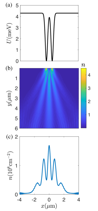
Introduction. Indirect excitons (IXs) in coupled quantum wells have emerged as a new platform for investigating quantum transport. The IXs have long lifetime, 1 long propagation distance, 2, 3, 4, 5, 6, 7, 8, 9 and long coherence length at temperatures below the temperature of quantum degeneracy [Eq. (7)]. 10 Although an IX is overall charge neutral, it can couple to an electric field via its static dipole moment , where is the distance between the electron and hole layers [Fig. 1(a)]. These properties enable experimentalists to study transport of quasi-equilibrium IX systems subject to artificial potentials controlled by external electrodes [Fig. 1(b)].
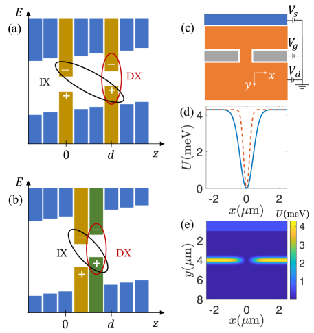
In this Letter, we examine theoretically the transport of IXs through nano-constrictions [Fig. 1(c-e)]. 11 Historically, studies of transmission of particles through narrow constrictions have led to many important discoveries. In particular, investigations of electron transport through so called quantum-point contacts (QPCs) have revealed that at low the conductance of smooth, electrostatically defined QPCs exhibits step-like behavior as a function of their width. 12, 13 The steps appear in integer multiples of (except for the anomalous first one 14) because the electron spectrum in the constriction region is quantized into one-dimensional (1D) subbands [Fig. 2(e)]. Here is the spin-valley degeneracy. Associated with such subbands are current density profiles analogous to the diffraction patterns of light passing through a narrow slit. These patterns have been observed by nanoimaging of the electron flow. 15 The conductance quantization has also been observed in another tunable fermionic system, a cold gas of atoms. 16
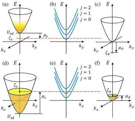
For the transport of bosonic IXs, we have in mind a conventional in solid-state physics setup where the QPC is connected to the source and drain reservoirs of unequal electrochemical potentials, and [Fig. 2(a-c)]. The difference is analogous to the source-drain voltage in electronic devices. Whereas electrons are fermions, IXs behave as bosons. This makes our transport problem unlike the electronic one. The problem is also different from the slit diffraction of photons or other bosons, such as phonons, considered so far. Indeed, one cannot apply a source-drain voltage to photons or phonons in any usual sense. [However, quantized heat transport of phonons 17, 18, 19 has been studied.]
To highlight the qualitative features, we do our numerical calculations for the case where the drain side is empty, . The conductance of the QPC can be described by the bosonic variant of the standard Landauer-Büttiker theory. 20 It predicts that the contribution of a given subband to the total conductance can exceed if its Bose-Einstein occupation factor is larger than unity. 21 To the best of our knowledge, there have been no direct experimental probes of this prediction in bosonic systems. The closest related experiment is probably the study of atoms passing through a QPC in the regime of enhanced attractive interaction. 22 That experiment has demonstrated the conductance exceeding and the theory 23, 24, 25 has attributed this excess to the virtual pairing of fermionic atoms into bosonic molecules by quantum fluctuations.
Below we present our theoretical results for the IX transport through single, double, and multiple QPCs. We ignore exciton-exciton interaction but comment on possible interaction effects at the end of the Letter.
Model of a QPC. In the absence of external fields, the IXs are free to move in a two-dimensional (2D) – plane. When an external electric field is applied in the -direction [Fig. 1(a)], an IX experiences the energy shift . This property makes it possible to create desired external potentials acting on the IXs. To engineer a QPC, needs to have a saddle-point shape. Such a potential can be created using a configuration of electrodes: a global bottom gate plus a few local gates on top of the device. As depicted in Fig. 1(b), two of such top electrodes (gray) can provide the lateral confinement and another two (blue and orange) can control the potential at the source and the drain. More electrodes can be added if needed. Following previous work, 11 in our numerical simulations we use a simple model for :
| (1) |
where is the Fermi function. The width parameters and and the coefficients and on the first line of Eq. (1) are tunable by the gate voltage [Fig. 1(b)]. The second line in Eq. (1) represents a gradual potential drop of magnitude , central coordinate , and a characteristic width in the -direction. These parameters are controlled by voltages and . Examples of are shown in Fig. 1(c,d).
For qualitative discussions, we also consider the model of a quasi-1D channel of a long length and a parabolic confining potential. The corresponding is obtained by replacing the top line of Eq. (1) with
| (2) |
where . The energy subbands [Fig. 2(b)] in such a channel are
| (3) |
The associated eigenstates are the products of the plane waves and the harmonic oscillator wavefunctions
| (4) |
where is the Hermite polynomial of degree . The length and frequency are given by
| (5) |
The subband energy spacing can be estimated as
| (6) |
which is approximately for devices made of transition metal dichalcogenides (TMDs), where exciton effective mass and . Hence, the onset of quantization occurs at . The same characteristic energy scales in GaAs quantum well devices, 11 can be obtained in a wider QPC, , taking advantage of the lighter mass, , cf. solid and dashed lines in Fig. 1(d). In both examples is much smaller than the IX binding energy ( in TMDs 26 and in GaAs 27, 28). Therefore, we consider the approximation ignoring internal dynamics of the IXs as they pass through the QPC 29 and treat them as point-like particles. Incidentally, we do not expect any significant reduction of the exciton binding energy due to many-body screening in the considered low-carrier-density regime in semiconductors with a sizable gap and no extrinsic doping. (At high carrier densities, the screening effect can be substantial.30)
Conductance of a QPC. As with usual electronic devices, we imagine that our QPC is connected to semi-infinite source and drain leads (labeled by ). Inside the leads the IX potential energy tends to asymptotic values . Without loss of generality, we can take , as in Eq. (1). The difference is a linear function of the control voltages , [Fig. 1(b)]. The coefficient of proportionality can be estimated as , where is the vertical distance between the top and bottom electrodes. The IX energy dispersions at the source and the drain are parabolic and are shifted by with respect to one another, see Fig. 2(a, c). In the experiment, the IX density of the reservoirs can be controlled by photoexcitation power. For example, the IX density can be generated on the source side only, 11 while the drain side can be left practically empty, . This is the case we focus on below. The chemical potentials are related to the densities via 31, 32
| (7) |
Note that we count the chemical potentials from the minima of the appropriate energy spectra and that we use the units system . In turn, the electrochemical potentials are given by
| (8) |
which implies
| (9) |
In the terminology of electron devices, the first term in Eq. (9) is related to the source-drain voltage , \latinviz., . The second term in Eq. (9) is referred to as the built-in potential, which is said to originate from charge redistribution in the leads.
If the particle densities are fixed, variations of rigidly track those of . The differential conductance can be computed by taking the derivative of the source-drain particle current with respect to :
| (10) |
has dimension of and its natural quantum unit is . (The spin-valley degeneracy is in both TMDs and GaAs.)
For the long-channel model [Eq. (2)], can be calculated analytically because the single-particle transmission coefficients through the QPC have the form , i.e., they take values of either or . Here and is the Heaviside step-function. Adopting the standard Landauer-Büttiker theory for fermions 20 to the present case of bosons (see also 21), we find the total current to be where the partial currents are
| (11) |
and is the Bose function. In turn, the conductance is
| (12) |
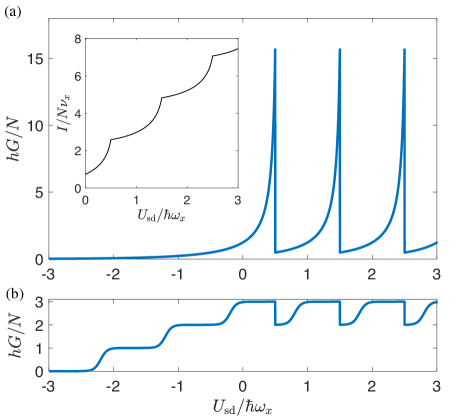
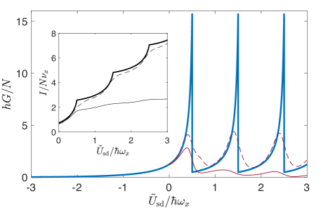
The dependence of on is illustrated in Fig. 3(a). The conductance exhibits asymmetric peaks. Each peak signals the activation of a new conduction channel whenever approaches the bottom of a particular 1D subband. All the peaks have the same shape, which is the mirror-reflected Bose function with a sharp cutoff. As decreases, the width of the peaks decreases. The magnitude of the peaks can be presented in the form
| (13) |
where is the occupation of the lowest energy state at the source. For fermions, is limited by . For 2D bosons, exceeds and, in turn, exceeds at .
The sudden drops of at [Fig. 3(a)] occur because the current carried by each subband saturates as soon as it becomes accessible to all the IXs injected from the source, down to the lowest energy . These constant terms do not affect the differential conductance . The total current as a function of is plotted in the inset of of Fig. 3(a).
It is again instructive to compare these results with the more familiar ones for fermions, which are obtained replacing the Bose function with the Fermi function in Eq. (12). In the regime where is large and negative, the Heaviside functions in Eq. (12) play no role, so that traces the expected quantized staircase shown in Fig. 3(b). The conductance steps occur whenever . Once approaches , a different behavior is found: the conductance displays additional sudden drops at , which causes it to oscillate between two quantized values. These drops appear for the same reason as in the bosonic case: current saturation for each subband that satisfies the condition .
The adiabatic QPC model considered above is often a good approximation 13, 12 for more realistic models, such as Eq. (1). The latter cannot be treated analytically but we were able to compute numerically, using the transfer matrix method 3 (see below). The results are presented in the Supporting Information. The main difference from the adiabatic case is that the conductance peaks are reduced in magnitude and broadened.
Density distribution in a QPC. In analogy to experiments with electronic QPCs, 15 it would be interesting to study quantized conduction channels by optical imaging of IX flow. Unlike electrons, IXs can recombine and emit light, so that the IX photoluminescence can be used for measuring their current paths. This motivates us to model the density distribution of IXs in the QPC. We begin with analytical considerations and then present our numerical results, Fig. 4.
The calculation of the involves two steps. First, we solve the Schrödinger equation for the single-particle energies and the wavefunctions of IXs subject to the potential . The boundary conditions for the is to approach linear combinations of plane waves of momenta at but contain no waves of momenta with at . Such states correspond to waves incident from the source. Second, we sum the products to obtain the . We choose not to multiply the result by , so that our is the IX density per spin per valley.
For a qualitative discussion, let us concentrate on the simplest case of large , i.e., fast particles. As the incident wave propagates from the source lead, it first meets the smooth potential drop at . Assuming , the over-the-barrier reflection at can be neglected. Therefore, the -momentum increases to the value dictated by the energy conservation,
| (14) |
while the -momentum remains the same. Subsequently, the incident wave impinges on the QPC at . Typically, this causes a strong reflection back to the source. However, certain eigenstates have a nonnegligible transmission. After passing the QPC, their wavefunctions expand laterally with the characteristic angular divergence of . Such wavefunctions can be factorized , where the slowly varying amplitude obeys the eikonal (or paraxial) equation
| (15) |
If the model of the long constriction [Eq. (2)] is a good approximation, the solution is as follows. Inside the QPC, is proportional to a particular oscillator wavefunction [Eq. (4)]. Outside the QPC, it behaves as a Hermite-Gaussian beam whose probability density can be written in the scaling form
| (16) | ||||
| (17) | ||||
| (18) |
This representation has been used in the study of a Bose-Einstein condensate (BEC) expansion from a harmonic trap. 34, 35 Our problem of the steady-state 2D transport through the QPC maps to the noninteracting limit of this problem in D, with playing the role of time. In other words, the IX current emerging from the QPC is mathematically similar to a freely expanding BEC. This mapping is accurate if the characteristic width of the energy distribution of the IX injected into the QPC from the source is small enough, . Dimensionless function has the meaning of the expansion factor. A salient feature of the eigenfunctions are the nodal lines . The lowest subband has no such lines whereas the higher subbands have exactly of them.
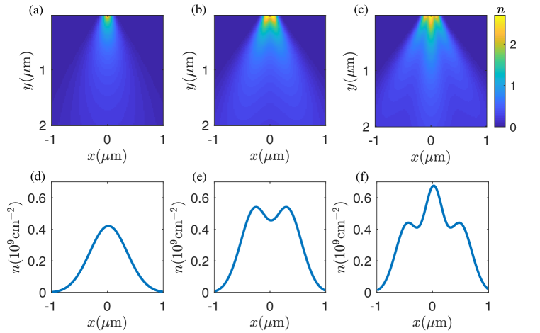
For a quantitative modeling, we carried out simulations using the transfer matrix method. 3 This method gives a numerical solution of the Schrödinger equation discretized on a finite-size real-space grid for a given energy and the boundary conditions described above. To obtain the total particle density, we summed the contributions of individual states, making sure to include enough ’s to achieve convergence. In all our calculations the chemical potential was fixed to produce the density (per spin per valley) at the source. Examples of such calculations for temperature are shown in Fig. 4. Since the partial densities are weighted with the Bose-Einstein factor , the lowest-energy subband typically dominates the total density, making it look like a nodeless Gaussian beam [Fig. 4(a,d)]. However, if is tuned slightly above the bottom of the subband, the contribution of this subband is greatly enhanced by the van Hove singularity of the 1D density of states inside the QPC. As a result, develops a valley line (local minimum) at , which is the nodal line of function [Fig. 4(b,e)]. A similar phenomenon occurs when we tune to slightly above the bottom of subband. Here the density exhibits two valley lines, which approximately follow the nodal lines of function [Fig. 4(c,f)]. These theoretical predictions may be tested by imaging IX emission with high enough optical resolution. Note that these van Hove singularities do not enhance the differential conductivity because of the cancellation between the density of states and the particle velocity . As explained above, this leads to current saturation and thus negligible contribution of th subband to at .
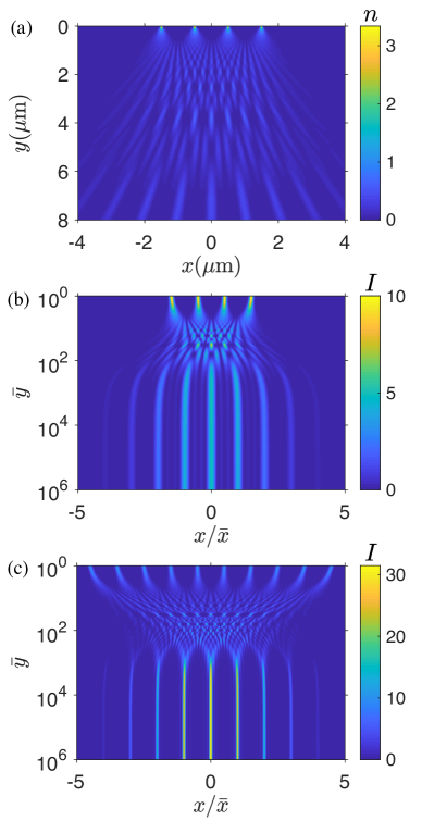
Double and multiple QPC devices. We have next explored the exciton analog of the Young double-slit interference. A short distance downstream from the first QPC ( along ), we added another potential barrier constructed from two copies of the single-QPC potential [Eq. (1)] shifted laterally in . As in Young’s classical setup, the first QPC plays the role of a coherent source for the double-QPC. An example of the latter with the center-to-center separation of is shown in Fig. 5(a). We computed the IX density distribution in this system for at which the IXs fluxes through all the QPCs are dominated by the subband. The IXs transmitted through the double-QPC create distinct interference fringes, Fig. 5(b,c).
Finally, we considered a four-QPC array. To show the results more clearly, we simulated the zero-temperature limit, where a single energy contributes. As illustrated by Fig. 6(a), the interference pattern begins to resemble that of a diffraction grating. Near the QPCs, it exhibits the periodic refocusing known as the Talbot effect. The repeat distance for the complete refocusing is 36
| (19) |
where is the de Broglie wavelength of the IXs and is the distance between the QPCs. For and , this distance is beyond the range plotted in Fig. 6(a). Therefore, only the so-called fractional Talbot effect is seen in that Figure. Although too fine for conventional imaging, these features may in principle be resolved by near-field optical techniques. Note that for a grating with slits the crossover to the far-field diffraction occurs at the distance , which is prohibitively large for the transfer matrix simulations. For a qualitative illustration of this crossover, we computed the interference pattern simply by adding a number of Gaussian beams, see Fig. 6(b,c).
Discussion and outlook. In this Letter, we considered a few prototypical examples of mesoscopic IX phenomena. We analyzed the subband quantization of IX transport through a single QPC, the double-slit interference from two QPCs, and the Talbot effect in multiple QPCs. As for electrons, these phenomena should be experimentally observable at low enough temperatures. The present theory may be straightforwardly expanded to more complicated potential landscapes and structures.
In the present work we neglected IX interactions. This interaction is dipolar, which in 2D is classified as short-range, parametrized by a certain interaction constant . As mentioned above, the problem of the IX transport through a QPC is closely related to the problem of a BEC expansion from a harmonic trap. Following the studies of the latter, 34 interaction can be included at the mean-field level by using the Gross-Pitaevskii equation instead of the Schrödinger one. For the single-QPC case, we expect the GPE solution to show a faster lateral expansion of the exciton “jet”, i.e., a more rapid growth of function . For the double- and multi-QPC cases, we expect repulsive interaction to suppress the interference fringes, similar to what is observed in experiments with cold atoms. 38 The lineshape and amplitude (visibility) of the fringes remain to be investigated.
Applications of our theory to real semiconductor systems would also require taking into account spin and valley degrees of freedom of IXs. It would be interesting to study spin transport of IXs 5, 10, 9 through nano-constrictions and associated spin textures. This could be an alternative pathway to probing spin conductance of quasi-1D channels. 39
The field of mesoscopic exciton systems is currently in its infancy but it is positioned to grow, extending the phenomena studied in voltage-controllable electron systems to bosons. More importantly, it has the potential to reveal brand new phenomena. There are many intriguing subjects for future work.
AUTHOR INFORMATION
Corresponding Author:
∗E-mail: chx035@ucsd.edu
Notes
The authors declare no competing financial interest.
Supporting Information Available:
The Supporting Information includes: i) electrostatic simulations of GaAs and TMD IX devices ii) derivation of Eq. (12) iii) transport simulations by the transfer matrix method. This material is available free of charge via the Internet at http://pubs.acs.org.
ACKNOWLEDGEMENTS
The work at UCSD is supported by the National Science Foundation under Grant ECCS-1640173 and by the NERC, a subsidiary of Semiconductor Research Corporation through the SRC-NRI Center for Excitonic Devices.
References
- Lozovik and Yudson 1976 Lozovik, Y. E.; Yudson, V. I. A new mechanism for superconductivity: pairing between spatially separated electrons and holes. Journal of Experimental and Theoretical Physics 1976, 44, 389–397
- Hagn \latinet al. 1995 Hagn, M.; Zrenner, A.; Böhm, G.; Weimann, G. Electric-field-induced exciton transport in coupled quantum well structures. Applied Physics Letters 1995, 67, 232–234
- Gärtner \latinet al. 2006 Gärtner, A.; Holleitner, A. W.; Kotthaus, J. P.; Schuh, D. Drift mobility of long-living excitons in coupled GaAs quantum wells. Applied Physics Letters 2006, 89, 052108
- Hammack \latinet al. 2009 Hammack, A. T.; Butov, L. V.; Wilkes, J.; Mouchliadis, L.; Muljarov, E. A.; Ivanov, A. L.; Gossard, A. C. Kinetics of the inner ring in the exciton emission pattern in coupled GaAs quantum wells. Physical Review B 2009, 80, 155331
- Leonard \latinet al. 2009 Leonard, J. R.; Kuznetsova, Y. Y.; Yang, S.; Butov, L. V.; Ostatnicky, T.; Kavokin, A.; Gossard, A. C. Spin transport of excitons. Nano Letters 2009, 9, 4204–4208
- Lazić \latinet al. 2010 Lazić, S.; Santos, P.; Hey, R. Exciton transport by moving strain dots in GaAs quantum wells. Physica E: Low-dimensional Systems and Nanostructures 2010, 42, 2640–2643
- Alloing \latinet al. 2012 Alloing, M.; Lemaître, A.; Galopin, E.; Dubin, F. Nonlinear dynamics and inner-ring photoluminescence pattern of indirect excitons. Physical Review B 2012, 85, 245106
- Lazić \latinet al. 2014 Lazić, S.; Violante, A.; Cohen, K.; Hey, R.; Rapaport, R.; Santos, P. Scalable interconnections for remote indirect exciton systems based on acoustic transport. Physical Review B 2014, 89, 085313
- Finkelstein \latinet al. 2017 Finkelstein, R.; Cohen, K.; Jouault, B.; West, K.; Pfeiffer, L. N.; Vladimirova, M.; Rapaport, R. Transition from spin-orbit to hyperfine interaction dominated spin relaxation in a cold fluid of dipolar excitons. Physical Review B 2017, 96, 085404
- High \latinet al. 2012 High, A. A.; Leonard, J. R.; Hammack, A. T.; Fogler, M. M.; Butov, L. V.; Kavokin, A. V.; Campman, K. L.; Gossard, A. C. Spontaneous coherence in a cold exciton gas. Nature 2012, 483, 584
- Dorow \latinet al. 2018 Dorow, C.; Leonard, J.; Fogler, M.; Butov, L.; West, K.; Pfeiffer, L. Split-gate device for indirect excitons. Applied Physics Letters 2018, 112, 183501
- Wharam \latinet al. 1988 Wharam, D. A.; Thornton, T. J.; Newbury, R.; Pepper, M.; Ahmed, H.; Frost, J. E. F.; Hasko, D. G.; Peacock, D. C.; Ritchie, D. A.; Jones, G. A. C. One-dimensional transport and the quantisation of the ballistic resistance. Journal of Physics C: Solid State Physics 1988, 21, L209
- Van Wees \latinet al. 1988 Van Wees, B.; Van Houten, H.; Beenakker, C.; Williamson, J. G.; Kouwenhoven, L.; Van der Marel, D.; Foxon, C. Quantized conductance of point contacts in a two-dimensional electron gas. Physical Review Letters 1988, 60, 848
- Micolich 2013 Micolich, A. Double or nothing? Nature Physics 2013, 9, 530–531
- Topinka \latinet al. 2000 Topinka, M.; LeRoy, B.; Shaw, S.; Heller, E.; Westervelt, R.; Maranowski, K.; Gossard, A. Imaging coherent electron flow from a quantum point contact. Science 2000, 289, 2323–2326
- Krinner \latinet al. 2015 Krinner, S.; Stadler, D.; Husmann, D.; Brantut, J.-P.; Esslinger, T. Observation of quantized conductance in neutral matter. Nature 2015, 517, 64
- Schwab \latinet al. 2000 Schwab, K.; Henriksen, E.; Worlock, J.; Roukes, M. L. Measurement of the quantum of thermal conductance. Nature 2000, 404, 974
- Gotsmann and Lantz 2013 Gotsmann, B.; Lantz, M. A. Quantized thermal transport across contacts of rough surfaces. Nature Materials 2013, 12, 59
- Cui \latinet al. 2017 Cui, L.; Jeong, W.; Hur, S.; Matt, M.; Klöckner, J. C.; Pauly, F.; Nielaba, P.; Cuevas, J. C.; Meyhofer, E.; Reddy, P. Quantized thermal transport in single-atom junctions. Science 2017, 355, 1192–1195
- Büttiker \latinet al. 1985 Büttiker, M.; Imry, Y.; Landauer, R.; Pinhas, S. Generalized many-channel conductance formula with application to small rings. Physical Review B 1985, 31, 6207–6215
- Papoular \latinet al. 2016 Papoular, D.; Pitaevskii, L.; Stringari, S. Quantized conductance through the quantum evaporation of bosonic atoms. Physical Review A 2016, 94, 023622
- Krinner \latinet al. 2016 Krinner, S.; Lebrat, M.; Husmann, D.; Grenier, C.; Brantut, J.-P.; Esslinger, T. Mapping out spin and particle conductances in a quantum point contact. Proceedings of the National Academy of Sciences 2016, 113, 8144–8149
- Kanász-Nagy \latinet al. 2016 Kanász-Nagy, M.; Glazman, L.; Esslinger, T.; Demler, E. A. Anomalous Conductances in an Ultracold Quantum Wire. Phys. Rev. Lett. 2016, 117, 255302
- Uchino and Ueda 2017 Uchino, S.; Ueda, M. Anomalous Transport in the Superfluid Fluctuation Regime. Phys. Rev. Lett. 2017, 118, 105303
- Liu \latinet al. 2017 Liu, B.; Zhai, H.; Zhang, S. Anomalous conductance of a strongly interacting Fermi gas through a quantum point contact. Phys. Rev. A 2017, 95, 013623
- Latini \latinet al. 2017 Latini, S.; Winther, K. T.; Olsen, T.; Thygesen, K. S. Interlayer Excitons and Band Alignment in MoS2/hBN/WSe2 van der Waals Heterostructures. Nano Letters 2017, 17, 938–945
- Szymanska and Littlewood 2003 Szymanska, M. H.; Littlewood, P. B. Excitonic binding in coupled quantum wells. Physical Review B 2003, 67, 193305
- Sivalertporn \latinet al. 2012 Sivalertporn, K.; Mouchliadis, L.; Ivanov, A. L.; Philp, R.; Muljarov, E. A. Direct and indirect excitons in semiconductor coupled quantum wells in an applied electric field. Physical Review B 2012, 85, 045207
- Grasselli \latinet al. 2016 Grasselli, F.; Bertoni, A.; Goldoni, G. Exact two-body quantum dynamics of an electron-hole pair in semiconductor coupled quantum wells: A time-dependent approach. Physical Review B 2016, 93, 195310
- Kharitonov and Efetov 2008 Kharitonov, M. Y.; Efetov, K. B. Electron screening and excitonic condensation in double-layer graphene systems. Phys. Rev. B 2008, 78, 241401
- Remeika \latinet al. 2015 Remeika, M.; Leonard, J. R.; Dorow, C. J.; Fogler, M. M.; Butov, L. V.; Hanson, M.; Gossard, A. C. Measurement of exciton correlations using electrostatic lattices. Phys. Rev. B 2015, 92, 115311
- Ivanov \latinet al. 1999 Ivanov, A. L.; Littlewood, P. B.; Haug, H. Bose-Einstein statistics in thermalization and photoluminescence of quantum-well excitons. Phys. Rev. B 1999, 59, 5032–5048
- Usuki \latinet al. 1995 Usuki, T.; Saito, M.; Takatsu, M.; Kiehl, R. A.; Yokoyama, N. Numerical analysis of ballistic-electron transport in magnetic fields by using a quantum point contact and a quantum wire. Physical Review B 1995, 52, 8244–8255
- Kagan \latinet al. 1996 Kagan, Y.; Surkov, E. L.; Shlyapnikov, G. V. Evolution of a Bose-condensed gas under variations of the confining potential. Physical Review A 1996, 54, R1753
- Castin and Dum 1996 Castin, Y.; Dum, R. Bose-Einstein condensates in time dependent traps. Physical Review Letters 1996, 77, 5315
- Rayleigh 1881 Rayleigh, L. XXV. On copying diffraction gratings and some phenomena connected therewith. Phil. Mag. 1881, 11, 196–205
- Juffmann \latinet al. 2013 Juffmann, T.; Ulbricht, H.; Arndt, M. Experimental methods of molecular matter-wave optics. Rep. Prog. Phys. 2013, 76, 086402
- Kohstall \latinet al. 2011 Kohstall, C.; Riedl, S.; Sánchez Guajardo, E. R.; Sidorenkov, L. A.; Denschlag, J. H.; Grimm, R. Observation of interference between two molecular Bose-Einstein condensates. New J. Phys. 2011, 13, 065027
- Meier and Loss 2003 Meier, F.; Loss, D. Magnetization Transport and Quantized Spin Conductance. Physical Review Letters 2003, 90, 167204
Supporting information
0.0.1 Electrostatic simulations
To better assess the practicality of the proposed IX devices, we numerically modeled several systems of the type shown in Fig. 1(a) of the main text. The first example we considered is a TMD heterostructure with the following layer sequence. First, there is a thin crystal of hBN, which serves as both the encapsulating layer and the gate dielectric. Next, there are MoS2 monolayers with two monolayers of hBN in between. Finally, there is a thicker hBN capping layer. Assuming the effective electron-hole separation is equal to the center-to-center distance of the two MoS2 layers and using and for the inter-layer spacing of, respectively, hBN and MoS2, we get in this design. We took the thickness of the lower hBN layer to be , corresponding to about atomic layers, and the total thickness of the structure to be . The structure is assumed to reside on a ground plane, e.g., a graphite substrate, and to possess a set of top gates depicted in Fig. 1(c) of the main text. Specifically, two symmetrically placed slits shaped as square hairpins ( and ), divide the top plane into two rectangular side gates maintained at voltage plus a narrow-necked central gate kept at voltage .
To compute the electrostatic potential distribution in this system we used a commercial finite-element solver. 1 Note that both hBN and MoS2 are materials with anisotropic permittivities 2 , and , . To simplify the simulations, we assigned MoS2 the same permittivities as hBN. In doing so, neglecting the difference of the in-plane permittivities is justified because the IX potential is determined by the -field. However, it is necessary to account for the difference of the -axis permittivities, which we did by multiplying the calculated by the factor
| (S1) |
Here is the fraction of the distance occupied by the hBN spacer. We found that a reasonably close fit to plotted by the dashed line in Fig. 1(d) of the main text can be achieved if the width of the side gates is , the width of the slits is as well, and the width of the neck of the central gate is . Such dimensions are attainable with standard nanofabrication methods. The applied voltages need to be on the central gate and on the side gates.
The second example we studied is an GaAs/AlGaAs heterostructure composed of of undoped AlGaAs, followed by two --thick GaAs quantum wells separated by a --thick AlGaAs barrier, capped by another undoped AlGaAs layer to the total thickness of . The center-to-center quantum well distance in this case is . The usual choice of the bottom electrode is an -GaAs substrate. We treated both GaAs and AlGaAs as isotropic materials with identical permittivity of . We found that the potential shown by the solid line in Fig. 1(d) can be realized for the following electrode dimensions: width , slit width , central neck width . The applied voltages are and . Realizing this design again appears to be a straightforward task.
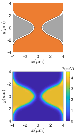
Finally, we simulated the potential produced in the same GaAs/AlGaAs heterostructure by a different top electrode pattern, in which the slits delineating the side electrodes are curved, Fig. S1(a). The computed is plotted in Fig. S1(b). This design gives a better approximation to an ideal adiabatic QPC, see below.
0.0.2 Derivation of Eq. (12)
The quasiparticle velocity of th subband is
| (S2) |
Therefore, the current injected by the source into the subband is
| (S3) |
which agrees with Eq. (11) of the main text. Here , label the bosonic and fermionic cases, respectively. The current injected by the drain is computed similarly. For an adiabatic QPC with the transmission coefficients , the net current of th subband is
| (S4) |
Accordingly, the differential conductance defined by Eq. (10) of the main text can be written as
| (S5) |
where
| (S6) |
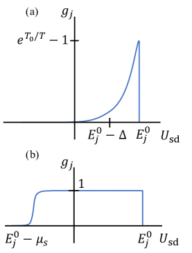
is the dimensionless conductance of subband . This quantity depends on the same way as the mirror-reflected quasiparticle occupation factor until reaches , at which point drops to zero, see Fig. S3. As explained in the main text, the reason for this cutoff behavior is that the current contributed by channel remains constant if increases past the subband bottom . Therefore, it does not affect the differential conductance. However, if the QPC is not perfectly adiabatic, the transmission coefficient has a gradual rather than the sharp onset at , and so the cutoff of at is also gradual (see below). Finally, summing over all the subbands, we obtain the total differential conductance shown in Fig. 3 of the main text.
0.0.3 Transport simulations
To calculate the conductance of a bosonic QPC, we used the transfer matrix method. 3 In this method the 2D Schrödinger equation with energy and potential in the simulation region is represented by a tight-binding model on a square lattice with a suitably small lattice constant . We take and , giving us a simulation grid with points along the -axis. The boundary conditions for the Schrödinger equation correspond to semi-infinite leads inside which the particles are subject to -independent potentials
| (S7) |
for the source and the drain, respectively. The energy spectrum of the source lead consists of subbands with dispersion . Here are the quantized energies of motion in the potential ,
| (S8) |
is the kinetic energy of the -motion, and is the -axis momentum. The -axis velocity is
| (S9) |
Similar energy spectrum exists in the drain. The transfer matrix algorithm computes the matrix of the transmission coefficients between every subband of the source and every subband of the drain. To reduce the computation load, we did not explicitly include the potential drop in . As explained in the main text, this drop simply changes the particle velocity. We accounted for it by including the ratio of velocities before and after the drop as a multiplicative factor. Accordingly, our formula for the total current injected into the QPC by the subband of the source is
| (S10) |
The -grid in the summation must be dense enough to achieve accuracy. We found the following choice adequate:
| (S11) |
The net current through the QPC for the case of empty drain is simply .
For consistency check, consider first an ideal adiabatic QPC, where the transmission coefficients are . The rule for changing variables from to is found from the energy conservation
| (S12) |
which entails
| (S13) |
Using these expressions, it is easy to see that Eq. (S10) is indeed transformed to Eq. (S3) in this limit. The corresponding analytical results for the current and conductance as functions of are plotted in Fig. S3 by the thick lines. Shown in the same Figure by the dashed lines are our numerical results for the potential of Fig. (S1)(b). They prove to be fairly close to the adiabatic limit except for some rounding of the conductance peaks and the current steps, as expected. On the other hand, the results for the potential given by Eq. (1) of the main text, which are indicated by the thin lines, deviate more from the ideal case.
References
- 1 COMSOL Multiphysics® v. 4.0. http://www.comsol.com
- Fogler \latinet al. 2014 Fogler, M. M.; Butov, L. V.; Novoselov, K. S. High-temperature superfluidity with indirect excitons in van der Waals heterostructures. Nature Communications 2014, 5, 4555
- Usuki \latinet al. 1995 Usuki, T.; Saito, M.; Takatsu, M.; Kiehl, R. A.; Yokoyama, N. Numerical analysis of ballistic-electron transport in magnetic fields by using a quantum point contact and a quantum wire. Physical Review B 1995, 52, 8244–8255