Observation of Complete Photonic Bandgap in Low Refractive Index Contrast Inverse Rod-Connected Diamond Structured Chalcogenides
Abstract
Three-dimensional complete photonic bandgap materials or photonic crystals block light propagation in all directions. The rod-connected diamond structure exhibits the largest photonic bandgap known to date and supports a complete bandgap for the lowest refractive index contrast ratio down to . We confirm this threshold by measuring a complete photonic bandgap in the infrared region in Sn–S–O and Ge–Sb–S–O inverse rod-connected diamond structures. The structures were fabricated using a low-temperature chemical vapor deposition process via a single-inversion technique. This provides a reliable fabrication technique of complete photonic bandgap materials and expands the library of backfilling materials, leading to a wide range of future photonic applications.
keywords:
direct laser writing, two-photon lithography, chemical vapor deposition, chalcogenide materials, photonic bandgap, three-dimensional photonic crystalsUniversity of Bristol] Department of Electrical and Electronic Engineering, University of Bristol, Merchant Venturers Building, Woodland Road, Bristol BS8 1UB, United Kingdom University of Southampton] Optoelectronics Research Centre, University of Southampton, University Road, Southampton SO17 1BJ, United Kingdom University of Southampton] Optoelectronics Research Centre, University of Southampton, University Road, Southampton SO17 1BJ, United Kingdom University of Southampton] Optoelectronics Research Centre, University of Southampton, University Road, Southampton SO17 1BJ, United Kingdom University of Bristol] Department of Electrical and Electronic Engineering, University of Bristol, Merchant Venturers Building, Woodland Road, Bristol BS8 1UB, United Kingdom University of Bristol] Department of Electrical and Electronic Engineering, University of Bristol, Merchant Venturers Building, Woodland Road, Bristol BS8 1UB, United Kingdom University of Bristol] Department of Electrical and Electronic Engineering, University of Bristol, Merchant Venturers Building, Woodland Road, Bristol BS8 1UB, United Kingdom Oxford Instruments Plasma Technology] Oxford Instruments Plasma Technology, North End, Yatton, Bristol BS49 4AP, United Kingdom University of Southampton] Optoelectronics Research Centre, University of Southampton, University Road, Southampton SO17 1BJ, United Kingdom University of Southampton] Optoelectronics Research Centre, University of Southampton, University Road, Southampton SO17 1BJ, United Kingdom University of Southampton] Optoelectronics Research Centre, University of Southampton, University Road, Southampton SO17 1BJ, United Kingdom University of Bristol] Department of Electrical and Electronic Engineering, University of Bristol, Merchant Venturers Building, Woodland Road, Bristol BS8 1UB, United Kingdom
Three-dimensional (3D) complete photonic bandgap (PBG) structures have been widely studied since their invention in 1987 by John1 and Yablonovitch.2 A complete PBG structure can prohibit photon propagation in any direction and this strong confinement of light can be exploited for applications ranging through high precision sensing,3 ultralow power and ultrafast optical switches,4 low threshold nanolasers,5 high efficiency single photon sources,6 and integrated photonic circuits.7 However, such 3D PBG materials are difficult to fabricate. Currently two main techniques of fabrication have been demonstrated: bottom-up and top-down. The bottom-up method refers to schemes where nano-objects self-assemble into structures that then exhibit a PBG.8, 9 The top-down approach refers to creating 3D structures using etching, ion-milling, lithography or laser writing that then produce PBGs.
Many of the top-down techniques involve miscellaneous fabrication steps such as wafer-fusion and micromanipulation,10, 11 while others such as single prism holographic lithography12, 13 do not allow for local modification for defects or waveguides. Alternatively, direct laser writing (DLW) using two-photon polymerization (2PP) allows for a variety of high refractive index contrast (RIC) 3D photonic crystal (PhC) structures with complete PBGs in near-infrared14 and visible15 regions to be realized. To fulfill the high RIC requirement high index material (silicon or titanium dioxide) needs to be deposited into 3D templates. Most deposition temperatures are above the polymer melting point hence double inversion methods16 or protective layers methods15 have been used to make complete PBG materials. There have also been successful demonstrations of DLW into photosensitive chalcogenide materials, followed by etching, showing bandgaps in the wavelength range.17, 18
In this work, we have developed a low temperature Chemical Vapor Deposition (CVD) of chalcogenide materials19, 20 to directly backfill unmodified polymer templates. Two materials were chosen for this work, Sn–S and Ge–Sb–S, due to their high refractive index values and low absorption in the near-infrared region, but also because they have attractive nonlinear optical properties suitable for applications, such as optical switches.20 The chalcogenide materials are conformally coated on polymeric RCD templates,21 which are written by a commercial DLW system (Nanoscribe GmbH). The chalcogenide/polymer structure is then exposed to an oxygen plasma, resulting in selective etching of the polymeric scaffold. This novel approach results in chalcogenide inverse RCD structures, and here, we successfully demonstrate measurements showing a complete PBG at near-infrared wavelength with low RIC ( for Sn–S–O/air and 2:1 for Ge–Sb–S–O/air) materials.
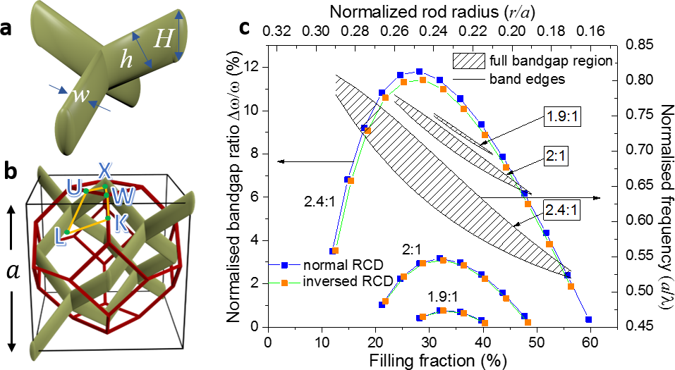
To achieve a complete PBG for smaller wavelengths, a higher PBG ratio (gap width to center wavelength ratio ) structure is required to minimize fabrication tolerance, that is, prevent errors from templates and depositions. The RCD structure,22 from the A7 crystal family,23 is reported to retain the highest complete PBG ratio among all crystal geometries and the lowest RIC () known to support a complete PBG.24, 25 This RCD structure is described as rods replacing bonds between atoms in a diamond crystal. The conventional cubic unit cell consists of four tetrahedrons (Figure 1a) stacked two by two in orthogonal directions (Figure 1b). The lattice constant, , is used to define an RCD structure (Figure 1b). For a realistic simulation of the fabricated samples, elliptical rods are preferred, with a width and a ”transverse height” (, where is the ”vertical height”; Figure 1a). The translational symmetry of an RCD (and its inversion) is the same as a face-centered cubic (FCC) structure, and the first Brillouin zone is a truncated octahedron (red line in Figure 1b). XWKLU are the symmetry points on the Brillouin zone in an RCD structure. A high-quality RCD is not a layered structure and, thus, cannot be easily achieved using layer-by-layer 2D lithography methods. Moreover, the rod diameter required for direct high-index RCD26 is below the 2PP DLW system resolution with a 780 laser. Fortunately, its inverse structure shows a slightly smaller PBG ratio of 11% (compared to 11.7 %) at the same RIC (2.4:1), material filling fraction (FF), and rod radius, as illustrated in Figure 1c. By utilizing this inverse structure, one can create a relatively low resolution (big rods) polymer template to realize an air-filled high index structure.
1 Results and Discussion
Using the MIT photonic band (MPB) software,27 based on the plane wave expansion method, we calculated the normal and inverse RCD’s photonic band structure. We also used Lumerical,28 a commercial-grade simulator based on the finite-difference time-domain (FDTD) method, to calculate their angular dependent reflection spectra. For the FDTD simulations, we used a plane wave as source and set it to different propagation angles (relative to the normal incidence) to create angular spectrum results. Substrates are not included in all calculations as the substrate thickness is far bigger than the photonic crystal thickness and it generates barely visible differences compared to the simulations without substrate, but hugely increases the required computational resources. Figure 1c plots the PBG ratio and the normalized frequency () of the PBG position as a function of the air rod radius (or high index material FF) in an inverse RCD structure. In this example, we assume rods are cylindrical and used three RICs 2.4:1, 2:1 and 1.9:1 (refractive index is averaged and nondispersive). A band structure calculation for inverse RCDs with RIC 2.4:1 at different FF (Figure 1c) shows the complete PBG only appears within the range of air rod radius from 0.175 to 0.3, with a corresponding FF of material from 60% to 10% and normalized frequency of PBG from to . The maximum complete PBG ratio is 11%, ranging from to , and appears with a 0.25 air rod radius. When reducing the RIC to 2:1 and 1.9, the FF and radius ranges to obtain a complete PBG decrease, while the PBG ratio decreases and the midgap frequency increases. However, the optimal radius stays around 0.23-0.25 for all three RICs. A practical resolution constant for the RCD structure is chosen, which results in the PBG wavelength range from to and around 500 diameter template rods. An optimized commercialized DLW system based on 2PP has shown voxel resolution down to lateral and vertical.29
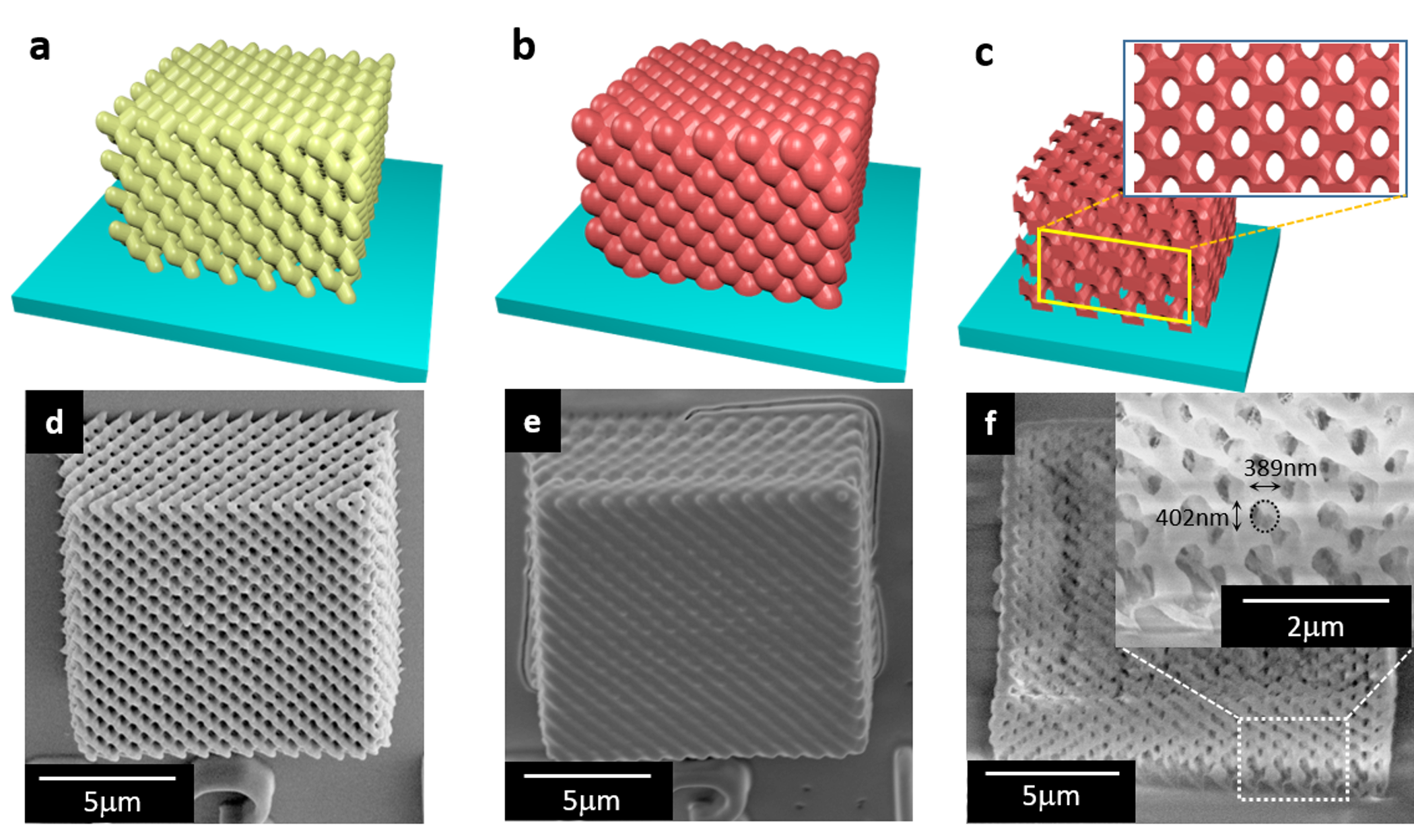
The fabrication of an inverse RCD structure can be described in three main phases: template construction, high index material backfilling, and polymer removal, shown in Figure 2. Phase one constructs a polymer RCD template (Figure 2a) using a 2PP DLW method (see Materials and Methods for the details). We followed the optimized rod radius based on the MPB simulations (Figure 1c). The fabricated template has 6 lattice periods in z-axis and 14 in x- and y-axes (Figure 2d). To examine the 3D structure quality, an optical characterization of the template is performed prior to the backfilling process. This is done using a home-built Fourier imaging spectroscopy setup30 (see Materials and Methods).
In phase two (Figure 2b), high refractive index chalcogenide materials (Sn–S or Ge–Sb–S) are conformally deposited into the polymer templates using an in-house built CVD system31 (see Materials and Methods). The deposition rate of the CVD materials is controlled by the ratios between precursors and reactive gas, chamber pressure, deposition temperature, and gas flow. The low melting point nature of the polymer template limits the deposition temperature to 200\celsius or below. The Sn–S deposition was carried out at room temperature whereas 150\celsius was used for Ge–Sb–S deposition. A Scanning Electron Microscope (SEM) photo of a fully backfilled Ge–Sb–S–polymer RCD structure is shown in Figure 2e.
The final phase three is polymer removal. In phase two, the high index material grows omni-directionally inside and on top of the polymer templates. We used focused ion beam (FIB) milling to cut a thin layer off the top, to expose the buried polymer beneath, enabling the oxygen plasma to access the polymer template from above. The oxygen plasma reacts with the polymer to form gaseous compounds that escape from the template, but this treatment also partially oxidizes the chalcogenides resulting in reduced refractive indexes (see Materials and Methods for the details). Once the polymer template is removed, the partially oxidized high index materials will remain forming an inverse RCD structure. Figure 2f shows the oblique view of a completed inverse RCD structure (Ge–Sb–S–O based) from SEM. Elliptical air gaps are visible in the cross section, with width and height (ascertained from the SEM measured and Figure 1a).
The photonic band structures of the polymer templates are measured using wide-angle Fourier imaging spectroscopy and compared with the FDTD simulations.30 The RCD template fabricated via the 2PP process is an air–polymer-based crystal, where the RIC is approximately 1:1.5. Figure 3 shows the angular reflection spectra comparison between measured polymer templates and simulations via FDTD.
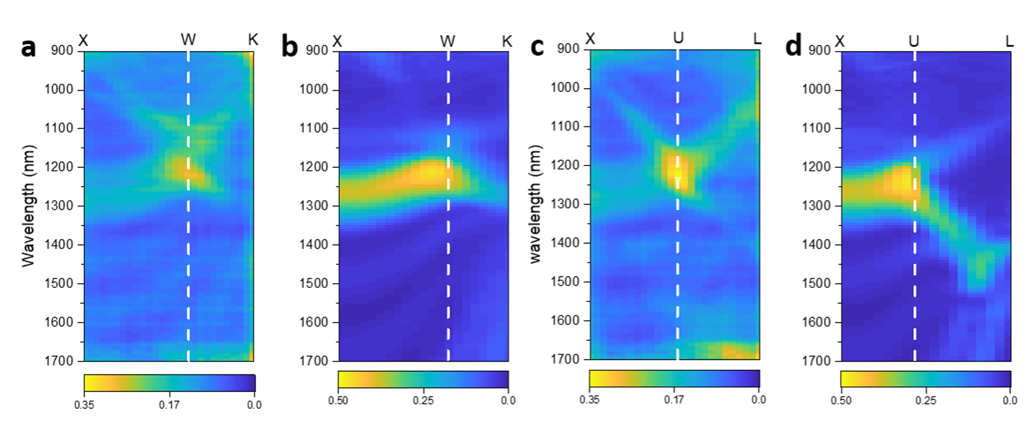
Figure 3a, b is the optical response (unpolarized reflection) for a detection angle in XUL and Figure 3c,d is for a detection angle in XWK. Figure 3a and c demonstrate partial band gaps with reflectivity above 20 % (30 % in simulation) at around wavelength in normal incidence angle (X) and blue-shifted reflection peaks at the second symmetry point (U and W, respectively), with reflectivity up to about 40 % in measurements and 50 % in FDTD simulation. FDTD simulations use structure parameters , , (slightly less than the targeted lattice size due to polymer shrinkage21), and finite 10 by 10 lattice periods in the x–y plane and 6 periods in the z-direction. The simulated fundamental bandgaps closely match the experimental results from the polymer template, with minor differences appearing only in higher order bands, demonstrating a high-quality template has been achieved.
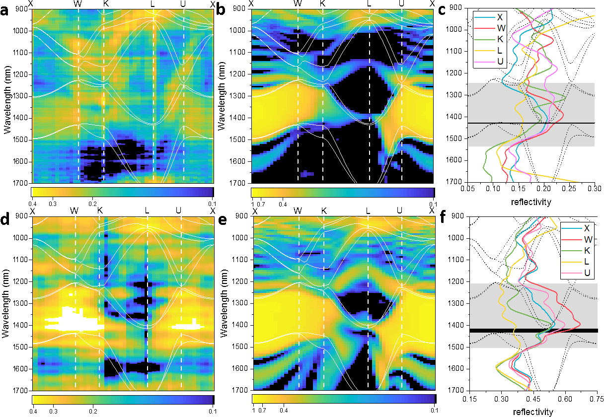
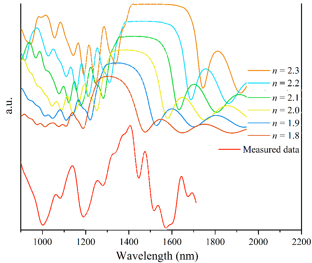
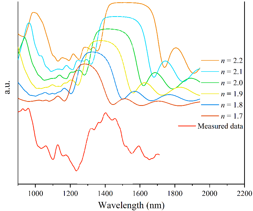
Figure 4a, d, b, and e show the optical response of the Sn–S–O (Ge–Sb–S–O) inverse RCDs in all symmetry points XWKLUX for measurement and FDTD simulation, respectively. MPB band structure calculations have been layered on top of all results in Figure 4. The refractive index of partially oxidized chalcogenides is estimated by using the energy-dispersive X-ray (EDX) spectroscopy technique to measure the material composition on both 3D structures and a test deposition on a wafer placed next to the sample in the deposition process. The dispersions of index for both materials are less than 0.1 in the range of , according to literature,31, 32 thus, we use averaged nondispersive refractive indexes for both materials in simulations. The resulting indexes are 1.9 for Sn–S–O and 2.0 for Ge–Sb–S–O at (see Materials and Methods for details).
In the measurement result for the Sn–S–O structure (Figure 4a), a continuous reflection peak (the fundamental PBG) across symmetry points X–W–K and L–U–X appears at around with reflectivity. The fundamental band reflectivity at K–L direction drops to around 15% due to the low RIC (1.9:1). Some higher order bands (reflection peaks) appear between in the W–K and U–X direction, matching its MPB simulation results. For the Ge–Sb–S–O structure measurement result in Figure 4d, a continuous reflection peak across all symmetry points appears at around , with a maximum 70 % reflectivity at the W direction and lowest reflectivity around 30 % at the L direction. Both FDTD simulations (Figure 4b, e) are based on finite size structures (10 lattices in the x–y plane). A small DC offset was applied to the color scale of measured data to suppress the background scattered light. The FDTD simulation parameters for the air rods are and for the Sn–S–O structure and and for Ge–Sb–S–O structure adjusted to best fit the optical results. This also confirms the values measured from the SEM results and supports our estimates of refractive indexes. The FDTD simulation shows lowered reflections in the peak (drop to less than 20 % reflectivity) at high observation angles (in the K–L region) due to the finite size (in the x–y plane) of the structures and edging effects, in contrast to the MPB (infinite structure size) calculations. For the same reasons, the measurements also show this effect, although there is a slight discontinuity seen around the L direction from a limitation of the imaging lens numerical aperture (NA). Figure 4c and f demonstrate the reflection spectra at each symmetry point for Sn–S–O and Ge–Sb–S–O structures, respectively. The overlapping reflection peaks at around for the Sn–S–O structure, and for the Ge–Sb–S–O structure indicate the appearance of complete bandgaps in both Sn–S–O (bandgap ratio ) and Ge–Sb–S–O (bandgap ratio ).
2 Conclusion
By introducing the single-inversion process using a low-temperature CVD technique, we demonstrate low RIC (Sn–S–O and Ge–Sb–S–O) inverse RCD structures with complete PBGs working in the near-infrared region for the first time. This single-inversion approach dramatically simplifies the 3D fabrication process. Using low-temperature CVD and removing polymer templates with oxygen plasma, we have shown it is possible to completely fill the nanoscale void space of 3D templates with chalcogenide materials. Optical modeling of the PBG material guided the design and, when compared with characterization results, enabled an estimation of device quality at each fabrication step. The complete PBGs ( and ) of inverse RCDs formed in low RIC (1.9:1 and 2:1), via Sn–S–O and Ge–Sb–S–O chalcogenide materials, were experimentally measured with results compared with numerical simulations using the FDTD technique and plane-wave expansion method. These results demonstrate the threshold of the lowest RIC supporting a complete PBG, experimentally validating results predicted by the topology optimization approach.25
These results open the way for developing a process to reliably fabricate arbitrary photonic bandgap structures in technologically relevant wavelength regions (). Moreover, our simulation work26 points the way toward micro/nanocavity designs capable of confining light in mode volumes down to cubic wavelengths.33 Our 3D lithography approach can be directly adapted to writing these cavity and waveguide structures, incorporating emitters to open new regimes of single photon level interactions,34 novel nanolasers5 and high-bandwidth, lossless, and subwavelength scale optical circuits.7
Future work will consider the fabrication of inverse RCD structures, along different growth directions (in particular, with the L direction aligned with the substrate normal) in order to measure the reflectivity at these higher angles more accurately. However, the accuracy will then be affected by structural differences due to the elliptical voxel shape and the ensuing required differences in writing technique.
3 Materials and Methods
3.1 Direct Laser Writing (DLW)
The DLW system is a commercial system from Nanoscribe GmbH, based on 2PP, which contains a femtosecond laser (pulse width and repetition rate ) and a high NA (= 1.4) oil immersion objective lens (, Zeiss). The laser writing power is set to 20% of mean output power (20 mW), with an adaptive piezo stage scanning speed of and three repetitions per line. The photoresist used is a liquid negative resist, IP-L 780 (Nanoscribe GmbH), drop-casted onto a glass substrate. An exposed template sample is developed using SU-8 developer for 30 min (to remove unpolymerized resist) and IPA for 5 min (to remove SU-8 developer).
3.2 Fourier Imaging Spectroscopy (FIS)
We used an identical system to that described in our previous work.30 This home-built Fourier imaging spectroscope uses a objective lens to collimate a fiber ( diameter) coupled white light source (Bentham Ltd. WLS100 ), focusing the light beam with an NA = 0.9, objective lens on the sample. The detection plane is a projection image for the backfocal plane of the objective lens. This image is scanned by a fiber ( diameter) attaches to a x–y motorized stage, the other end of the fiber connects to a spectrometer (Ocean optics NIRQuest512), which has spectrum range. The angular resolution of the system is per scan step.
3.3 Chemical Vapor Deposition (CVD)
For Sn–S deposition: (99.999% pure from Alfa Aesar) is used as the precursor to react with gas (99.9% pure from Air Liquide) to form Sn–S at room temperature with the chamber pressure of 100 mbar controlled by a Vacuubrand MV10NT diaphragm pump. A 30 mm O.D. 1000 mm long quartz tube is used for CVD reaction and the precursor, vapor, was delivered with gas through a mass flow controller (MFC) at 10 sccm, whereas gas was delivered through another MFC at 50 sccm.
For Ge–Sb–S deposition: (99.9999% pure from Umicore) and (99.999% pure from GWI) are used as the precursors to react with gas (99.9% pure from Air Liquide) to form Ge–Sb–S at 150\celsius with atmospheric chamber pressure. A 30 mm O.D. 1000 mm long quartz tube is used for CVD reaction and the precursors, and vapors, are delivered individually with gas through MFCs at 20 and 80 sccm, respectively, whereas gas is delivered through another MFC at 50 sccm.
3.4 Inductively Coupled Plasma (ICP) Etching
We used an ICP system, PlasmalabSystem 100 (ICP 180), from Oxford Instruments in the polymer removal process. The process was run twice for Sn–S structure and each time uses SEM to confirm complete removal of polymer template. The first run duration time was 5 min 30 s with 30 mTorr chamber pressure, oxygen flow rate was 50 sccm, and 100 W RF forward power and 400 W ICP forward power, reaction temperature was 60\celsius. The second run reduced duration to 5 min and chamber pressure to 20 mTorr, other settings unchanged. For Ge–Sb–S structure the ICP parameters changed to duration time 40 min, 30 mTorr chamber pressure, oxygen flow rate was 50 sccm, 20 W RF forward power and 400 W ICP forward power, reaction temperature decreased to 40\celsius to reduce etching rate.
3.5 Evaluation of the Refractive Index Values
The refractive index of planar chalcogenide films grown under identical conditions and exposed to similar plasma etching were evaluated by ellipsometry. However, these measurements yielded refractive index values that were far too high ( for GeSbS) to explain the optical measurements. It was suspected that this might be due to oxidation effects which would be confined to the surface in planar films, while our porous structures are effectively fully oxidized. EDX measurements of the composition of planar films confirmed limited oxidation. In contrast, EDX measured compositions of 3D RCD structures were and , showing significant oxygen uptake and suggesting much lower refractive index values around 2.0 and 1.9, respectively. This was further confirmed by using the refractive index (RI) values as a hand fitting parameter in the calculation of the expected reflection spectra at normal incidence using the FDTD method, as illustrated in Figures 5 and 6.
4 Funding
Engineering and Physical Sciences Research Council (EPSRC) (EP/M009033/1, EP/M008487/1, EP/M024458/1, EP/N00762X/1).
This work was carried out using the cleanroom fabrication facilities of the Centre for Nanoscience and Quantum Information (NSQI), University of Bristol, and the Optoelectronics Research Centre (ORC), University of Southampton, and computational facilities of the Advanced Computing Research Centre (ACRC), University of Bristol.
References
- John 1987 John, S. Strong localization of photons in certain disordered dielectric superlattices. Physical Review Letters 1987, 58, 2486–2489
- Yablonovitch 1987 Yablonovitch, E. Inhibited Spontaneous Emission in Solid-State Physics and Electronics. Physical Review Letters 1987, 58, 2059–2062
- Sünner et al. 2008 Sünner, T.; Stichel, T.; Kwon, S.-H.; Schlereth, T. W.; Höfling, S.; Kamp, M.; Forchel, A. Photonic crystal cavity based gas sensor. Applied Physics Letters 2008, 92, 261112
- Nozaki et al. 2010 Nozaki, K.; Tanabe, T.; Shinya, A.; Matsuo, S.; Sato, T.; Taniyama, H.; Notomi, M. Sub-femtojoule all-optical switching using a photonic-crystal nanocavity. Nature Photonics 2010, 4, 477–483
- Khajavikhan et al. 2012 Khajavikhan, M.; Simic, A.; Katz, M.; Lee, J. H.; Slutsky, B.; Mizrahi, A.; Lomakin, V.; Fainman, Y. Thresholdless nanoscale coaxial lasers. Nature 2012, 482, 204–207
- Aharonovich et al. 2011 Aharonovich, I.; Castelletto, S.; Simpson, D. A.; Su, C.-H.; Greentree, A. D.; Prawer, S. Diamond-based single-photon emitters. Reports on Progress in Physics 2011, 74, 76501
- John 2012 John, S. Why trap light? Nature Materials 2012, 11, 997
- Blanco et al. 2000 Blanco, A.; Chomski, E.; Grabtchak, S.; Ibisate, M.; John, S.; Leonard, S. W.; Lopez, C.; Meseguer, F.; Miguez, H.; Mondia, J. P.; Ozin, G. A.; Toader, O.; van Driel, H. M. Large-scale synthesis of a silicon photonic crystal with a complete three-dimensional bandgap near 1.5 micrometres. Nature 2000, 405, 437–440
- Galisteo-López et al. 2011 Galisteo-López, J. F.; Ibisate, M.; Sapienza, R.; Froufe-Pérez, L. S.; Blanco, Á.; López, C. Self-Assembled Photonic Structures. Advanced Materials 2011, 23, 30–69
- Aoki 2009 Aoki, K. Practical approach for a rod-connected diamond photonic crystal operating at optical wavelengths. Applied Physics Letters 2009, 95, 191910
- Aoki et al. 2003 Aoki, K.; Miyazaki, H. T.; Hirayama, H.; Inoshita, K.; Baba, T.; Sakoda, K.; Shinya, N.; Aoyagi, Y. Microassembly of semiconductor three-dimensional photonic crystals. Nature Materials 2003, 2, 117–121
- Park et al. 2011 Park, S.-G.; Miyake, M.; Yang, S.-M.; Braun, P. V. Cu2O Inverse Woodpile Photonic Crystals by Prism Holographic Lithography and Electrodeposition. Advanced Materials 2011, 23, 2749–2752
- Campbell et al. 2000 Campbell, M.; Sharp, D. N.; Harrison, M. T.; Denning, R. G.; Turberfield, A. J. Fabrication of photonic crystals for the visible spectrum by holographic lithography. Nature 2000, 404, 53
- Tétreault et al. 2006 Tétreault, N.; von Freymann, G.; Deubel, M.; Hermatschweiler, M.; Pérez-Willard, F.; John, S.; Wegener, M.; Ozin, G. a. New Route to Three-Dimensional Photonic Bandgap Materials: Silicon Double Inversion of Polymer Templates. Advanced Materials 2006, 18, 457–460
- Frölich et al. 2013 Frölich, A.; Fischer, J.; Zebrowski, T.; Busch, K.; Wegener, M. Titania Woodpiles with Complete Three-Dimensional Photonic Bandgaps in the Visible. Advanced Materials 2013, 25, 3588–3592
- Varghese et al. 2013 Varghese, L. T.; Fan, L.; Wang, J.; Xuan, Y.; Qi, M. Rapid and Low-Cost Prototyping of 3D Nanostructures with Multi-Layer Hydrogen Silsesquioxane Scaffolds. Small 2013, 9, 4237–4242
- Cumming et al. 2014 Cumming, B. P.; Turner, M. D.; Schröder-Turk, G. E.; Debbarma, S.; Luther-Davies, B.; Gu, M. Adaptive optics enhanced direct laser writing of high refractive index gyroid photonic crystals in chalcogenide glass. Opt. Express 2014, 22, 689–698
- Nicoletti et al. 2011 Nicoletti, E.; Bulla, D.; Luther-Davies, B.; Gu, M. Planar defects in three-dimensional chalcogenide glass photonic crystals. Optics Letters 2011, 36, 2248
- Freeman et al. 2008 Freeman, D.; Grillet, C.; Lee, M. W.; Smith, C. L.; Ruan, Y.; Rode, A.; Krolikowska, M.; Tomljenovic-Hanic, S.; de Sterke, C.; Steel, M. J.; Luther-Davies, B.; Madden, S.; Moss, D. J.; Lee, Y.-h.; Eggleton, B. J. Chalcogenide glass photonic crystals. Photonics and Nanostructures - Fundamentals and Applications 2008, 6, 3–11
- Hewak et al. 2010 Hewak, D. W.; Brady, D.; Curry, R. J.; Elliott, G.; Huang, C.-C.; Hughes, M.; Knight, K.; Mairaj, A.; Petrovich, M.; Simpson, R.; Smith, C.; Sproat, C. In Photonic glasses and glass-ceramics; Murugan, G. S., Ed.; Research Signpost, 2010; pp 29–102
- Chen et al. 2015 Chen, L.; Taverne, M. P. C.; Zheng, X.; Lin, J.-D.; Oulton, R.; Lopez-Garcia, M.; Ho, Y.-L. D.; Rarity, J. G. Evidence of near-infrared partial photonic bandgap in polymeric rod-connected diamond structures. Optics Express 2015, 23, 26565
- Chan et al. 1991 Chan, C. T.; Ho, K. M.; Soukoulis, C. M. Photonic Band Gaps in Experimentally Realizable Periodic Dielectric Structures. EPL (Europhysics Letters) 1991, 16, 563
- Chan et al. 1994 Chan, C.; Datta, S.; Ho, K.; Soukoulis, C. A 7 structure: A family of photonic crystals. Physical Review B 1994, 50, 1988–1991
- Maldovan and Thomas 2004 Maldovan, M.; Thomas, E. L. Diamond-structured photonic crystals. Nature Materials 2004, 3, 593–600
- Men et al. 2014 Men, H.; Lee, K. Y. K.; Freund, R. M.; Peraire, J.; Johnson, S. G. Robust topology optimization of three-dimensional photonic-crystal band-gap structures. Optics Express 2014, 22, 22632
- Taverne et al. 2016 Taverne, M. P. C.; Ho, Y.-L. D.; Zheng, X.; Liu, S.; Chen, L.-F.; Lopez-Garcia, M.; Rarity, J. G. Modelling defect cavities formed in inverse three-dimensional rod-connected diamond photonic crystals. EPL (Europhysics Letters) 2016, 116, 64007
- Johnson and Joannopoulos 2001 Johnson, S.; Joannopoulos, J. Block-iterative frequency-domain methods for Maxwell’s equations in a planewave basis. Optics express 2001, 8, 173–190
- 28 Lumerical Solutions, Inc. https://www.lumerical.com
- Hermatschweiler et al. 2007 Hermatschweiler, M.; Ledermann, A.; Ozin, G. a.; Wegener, M.; von Freymann, G. Fabrication of Silicon Inverse Woodpile Photonic Crystals. Advanced Functional Materials 2007, 17, 2273–2277
- Chen et al. 2017 Chen, L.; Lopez-Garcia, M.; Taverne, M. P. C.; Zheng, X.; Ho, Y.-L. D.; Rarity, J. Direct wide-angle measurement of a photonic band structure in a three-dimensional photonic crystal using infrared Fourier imaging spectroscopy. Optics Letters 2017, 42, 1584
- Huang et al. 2010 Huang, C. C.; Wu, C. C.; Knight, K.; Hewak, D. W. Optical properties of CVD grown amorphous Ge–Sb–S thin films. Journal of Non-Crystalline Solids 2010, 356, 281–285
- El-Nahass et al. 2002 El-Nahass, M.; Zeyada, H.; Aziz, M.; El-Ghamaz, N. Optical properties of thermally evaporated SnS thin films. Optical Materials 2002, 20, 159–170
- Taverne et al. 2018 Taverne, M. P. C.; Ho, Y.-L. D.; Zheng, X.; Chen, L.; Fang, C.-H. N.; Rarity, J. Strong light confinement in rod-connected diamond photonic crystals. Opt. Lett. 2018, 43, 5202–5205
- Kubo et al. 2010 Kubo, Y.; Ong, F. R.; Bertet, P.; Vion, D.; Jacques, V.; Zheng, D.; Dréau, A.; Roch, J.-F.; Auffeves, A.; Jelezko, F.; Wrachtrup, J.; Barthe, M. F.; Bergonzo, P.; Esteve, D. Strong Coupling of a Spin Ensemble to a Superconducting Resonator. Phys. Rev. Lett. 2010, 105, 140502