Novel 2D Plasmon Induced by Metal Proximity
Abstract
A new electromagnetic plasma mode has been discovered in the hybrid system formed by a highly conductive gate strip placed in proximity to the two-dimensional electron system. The new plasmon mode propagates along the gate strip with no potential nodes present in transverse direction. Its unique spectrum combines characteristic features of both gated and ungated 2D plasmons. The new plasma excitation has been found to exhibit anomalously strong interaction with light.
pacs:
73.23.-b, 73.63.Hs, 72.20.My, 73.50.MxThe problem of electromagnetic waves propagating along metallic wires was treated rigorously by Sommerfeld more than 100 years ago Sommerfeld . He demonstrated that plasmon polariton waves travel along the wires at the speed of light. In fact, it is these plasmon polariton waves that carry alternating signal along the modern power lines. Recently, it has been shown theoretically that if a highly conducting wire is placed very close to a much less conducting two-dimensional electron system (2DES), the hybrid system may support a new electromagnetic plasma mode Volkov:19 . Remarkably, this proximity plasmon mode differs significantly from both gated and ungated 2D plasma modes that have been known in the literature for over 50 years Stern ; Chaplik:72 ; Grimes:76 ; Allen:77 ; Theis:77 . Its dispersion is described by the following expression:
| (1) |
where is the 2D electron density, is the effective electron mass, is the distance between the gate and 2DES, is the width of the gate strip, is the plasmon wave vector directed along the infinite gate and is the effective dielectric permittivity of the surrounding medium. Remarkably, the spectrum (1) combines fundamental features of both gated () and ungated () plasmons.
In the presence of external magnetic field, , normal to the plane of the 2DES, there occurs hybridization between the cyclotron and the plasma motions, which leads to the proximity plasmon magnetodispersion:
| (2) |
where is the electron cyclotron frequency. It has been shown in Allen:83 ; Volkov:EMP that in a finite 2DES, two different types of plasmon modes exist — the cyclotron magnetoplasmon and the one-way edge magnetoplasmon. Importantly, the new proximity plasmon excitation does not exhibit the edge magnetoplasmon mode in the presence of magnetic field. For quantitative treatment of the novel 2D plasmon mode the reader is referred to Supplemental Material I.
There are two reasons for which the observation of proximity plasma mode has been hindered over the past years. Foremost, it is due to the fact that proximity plasmon has no charge density nodes in the direction perpendicular to the metal strip, which naturally makes the mode dark to the electromagnetic wave with transversely polarized electric field — a typical configuration used in all pioneering experiments in the field of 2D plasmonics Allen:77 ; Theis:77 ; Heitmann:84 ; Heitmann:91 . Secondly, the most common geometry considered in theoretical analysis has been that of a finite 2DES with an infinite 2D screening gate Fetter:86 . The configuration which is, in a sense, reciprocal to the one necessary to observe the proximity plasmon. In presented experiments, we succeeded in making manifest the long lost plasmon excitation.
The experiments were conducted on a single nm wide GaAs/AlGaAs quantum well structure with electron density in the range of . The quantum well was located at a distance of Å below the crystal surface. Based on the transport measurements, the electron mobility at K was estimated to be . To enable excitation of plasma waves, a metallic gate was lithographically formed on the top surface of the sample, as illustrated by the inset in Fig. 1. The width and the length of the gate were varied from m to m and from mm to mm, respectively. Grounding contacts were fabricated on both sides of the gate, mm away from the strip edge. The microwave radiation was guided into the cryostat through a coaxial cable and then coupled to the gate strip by means of a coplanar waveguide transmission line. The microwave frequency was varied in the range of to GHz. In order to detect microwave absorption, we employed a non-invasive optical technique Ashkinadze ; Kukushkin:02 . The technique is based on high sensitivity of recombinant photoluminescence spectrum of 2D electrons to the electron temperature. The photoluminescence spectrum was recorded with and without the excitation microwave radiation and then the absolute value of the difference between the two spectra was integrated over the entire spectral range. Since the resultant integral is directly proportional to the change in the 2D electron temperature, it was used as a measure of microwave absorption. Sample was immersed in a liquid helium cryostat with superconducting coil. The superconducting coil was used to produce magnetic field ( – T) normal to the sample surface. All the experiments were performed at a temperature of K.
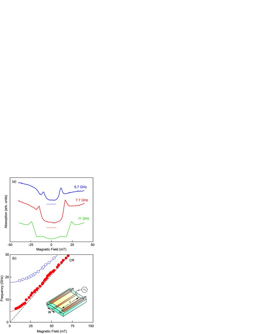
Figure 1 (a) illustrates microwave absorption measured in 2DES at , and GHz as a function of magnetic field . For these measurements there was used a structure with the gate strip dimensions mm and mm, and the 2D electron density, . The plotted data clearly indicate that there exists a pronounced absorption peak at each excitation frequency. The peak exhibits shift to higher values of magnetic field with microwave frequency increase. It was unexpected to find that the resonance arises at approximately GHz, which is considerably lower than predicted frequency of a gated plasmon Chaplik:72 :
| (3) |
According to Eq. (3), the frequency of the lowest gated plasmon mode with wave vector () is equal to GHz. Therefore, experimental results presented in Fig. 1(a) demonstrate that we have, in fact, observed a new 2D plasma excitation induced in 2DES by metal proximity.
Figure 1(b) displays the measured magnetodispersion of the new plasma mode. The red circles in the figure represent the data for the fundamental longitudinal proximity mode with transverse wave number . This set of data is closely approximated by the quadratic function from Eq. (2) plotted with red line. In the strong magnetic-field limit, the data tends to the cyclotron frequency asymptote shown with dashed line. From the fitted curve, the mode can be extrapolated to yield the plasma frequency at , GHz. This value is in excellent agreement with the theoretical prediction obtained from Eq. (1) for . This value of effective dielectric permittivity is very close to the average of the permittivity of GaAs and that of free space, for and .
Unlike the fundamental mode, the transverse plasma oscillations have potential nodes across the strip. The spectrum of the transverse modes in the limit of has been found in Volkov:19 as:
| (4) |
where () is the transverse component of the wave vector. Furthermore, in the long wavelength limit of , the expression in Eq. (4) reduces to an ordinary form describing a gated plasmon mode Eq. (3). It is this mode that has been observed in numerous experiments Eisenstein:00 ; Muravev:07 ; Andress:12 ; Koppens:18 , whereas the very fundamental plasma excitation with has been overlooked.
In addition to the fundamental mode, Fig. 1(b) includes measured dispersion data for the transverse proximity plasma mode with denoted by empty circles. Importantly, due to symmetric geometry of the E-field within the coplanar waveguide, used as an excitation feed, only the modes with even wave number, , can be excited in the given setup. As shown in the figure, the data can be extrapolated to estimate the mode frequency at to be GHz. The theoretical prediction for the transverse wave number, , based on Eq. (4) is found to be GHz. Such a minor discrepancy between experiment and the theoretical prediction can likely be ascribed to inaccurate description of the 2DES dielectric environment.
The most significant and remarkable feature of the newly discovered proximity plasmon mode is its square-root dispersion Volkov:19 . This is counter-intuitive, considering that a mode having 1D nature emerges in a gated 2DES system. It would be expected that both of these factors should favor linear dispersion law Kukushkin:05 ; Muravev:07 . Nevertheless, experimental results in Fig. 2 clearly indicate square root dispersion for the proximity plasmon mode. Therefore, in order to test the theory, the actual dispersion was measured for three samples of different strip length, and mm and fixed gate width, m. Fig. 2 displays the resultant experimental data, designated by red circles, along with the curve calculated using Eq. (1), plotted with a solid red line. It is evident from the figure that experimental results confirm the theoretical prediction of the square-root dispersion. The inset to Fig. 2 shows the measured proximity plasmon frequency as a function of parameter , in which case the measurements were performed on three samples of different gate width, and m and fixed gate length, mm. According to Eq. (1), is linearly proportional to . Hence, the obtained data are clearly in close agreement with the theoretical curve plotted with solid blue line.
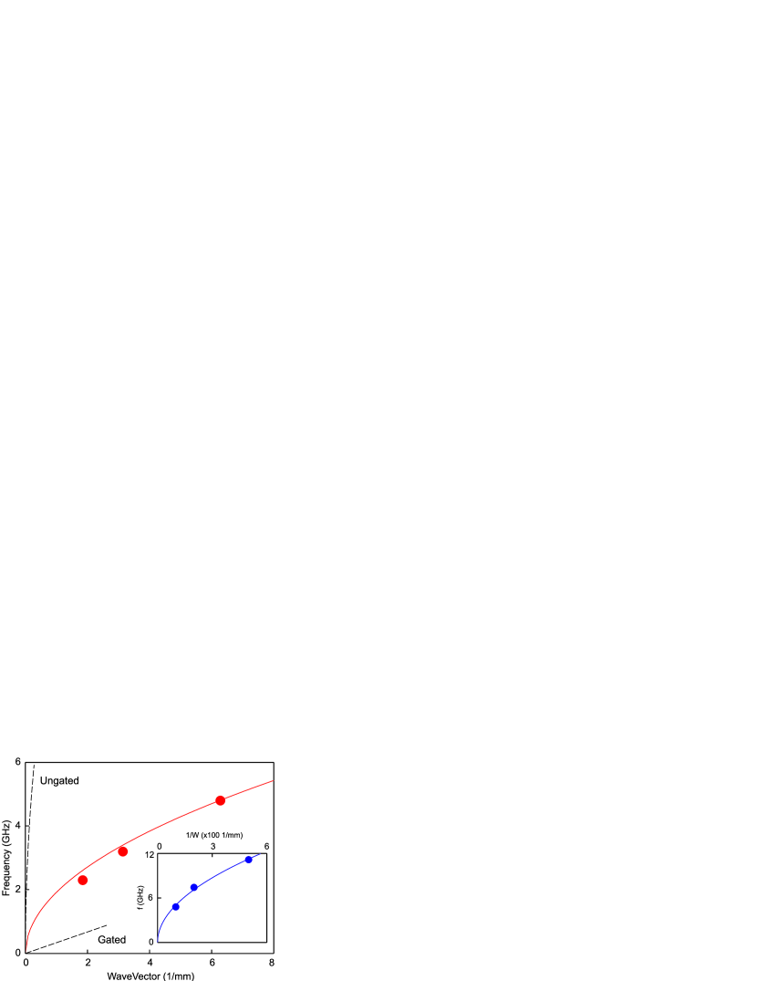
Concerning the experimental results in Fig. 2, it is worth noting that for the greatest gate strip length, mm, the measured data shows slight deviation from the square-root dispersion of approximately % . Such a reduction in plasmon resonant frequency for small wave vector values is a clear indication of hybridization between the plasma waves and the light. However, the magnitude of the observed hybridization far exceeds the level expected of the ordinary 2D plasmons Kukushkin:03 ; Kukushkin:06 ; Muravev:18 . According to theory for the ungated 2D plasmon, , where is a dimensionless retardation parameter defined as ratio of the plasmon frequency to that of light, given the same wave vector Muravev:18 . In essence, this parameter indicates the extent of the retardation effect. For the proximity plasmon mode under consideration, with mm, m, , which yields . Remarkably, the degree of coupling determined for the proximity plasmon experimentally is, in fact, times greater than that for the ungated 2D plasmon.
One of the most attractive properties of 2D plasmons is their tunability. In our experiments, we were able to tune the 2D electron density in the given structure using photodepletion method Kukushkin:89 . In Fig. 3 there are presented experimental results obtained for the sample with gate dimensions of m and mm. The spectral data in Fig. 3(a) illustrates that with decrease in electron concentration from to , the resonance peak shifts to the lower frequency. A more detailed dependence of the plasmon frequency on carrier density is shown in Fig. 3(b), where the measured data is compared against the theoretical curve that describes square-root dependence according to Eq. (1). The measured and calculated data, plotted with circles and solid line, respectively, show excellent agreement between experimental results and theory, demonstrating the possibility of tuning the speed of the new plasma mode over wide range.
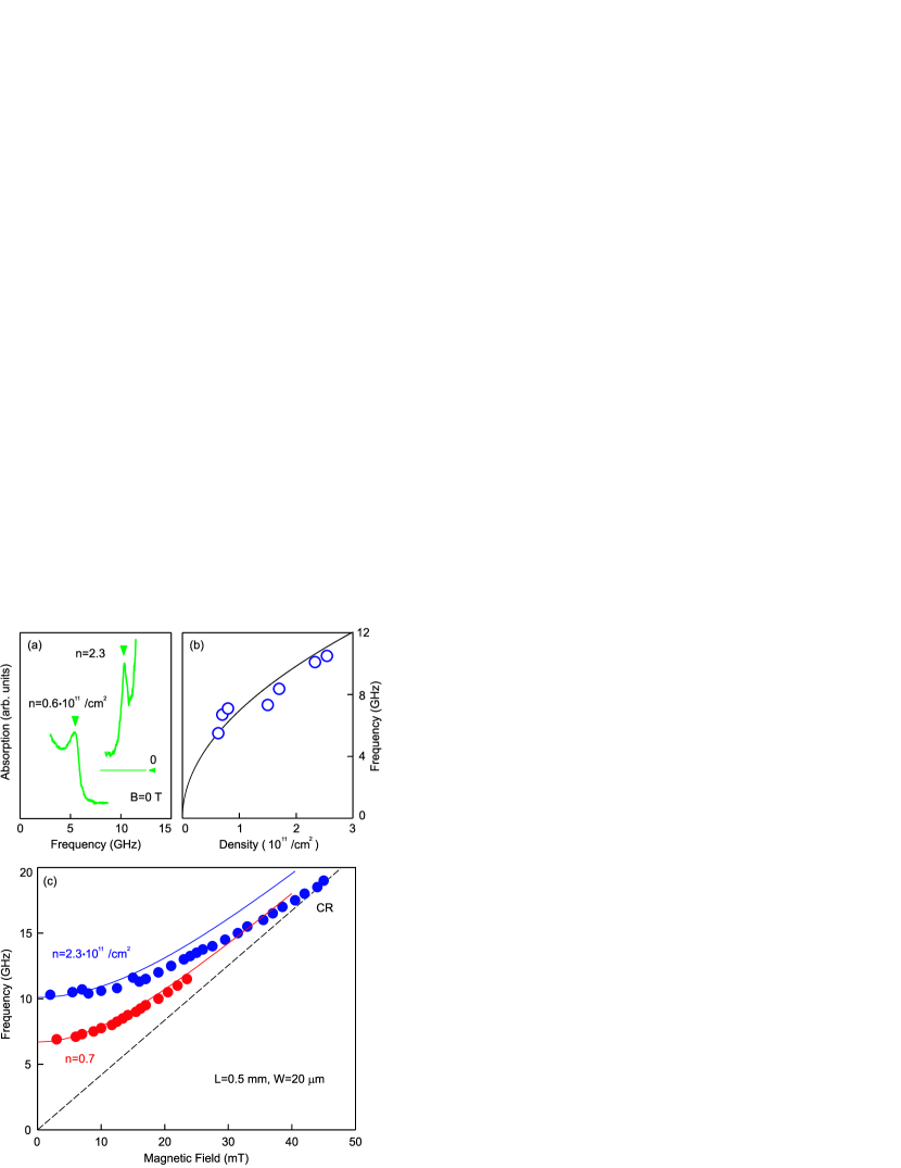
Figure 3(c) displays dependence of the proximity plasma mode frequency on magnetic field. The measurements were taken for the electron density of (red circles) and (blue circles). Experimental data closely follow the theoretical Pythagoras-like law, (solid lines). We observe that in the high-density limit of the magnetoplasma mode intersects the cyclotron resonance line. This again suggests the importance of the retardation effects viz. strong plasmon-photon coupling. Note that there was observed no influence of retardation effects on the proximity plasmon spectrum obtained for the sample with the same gate strip length, mm, but times greater width, mm, as shown in Fig. 1(b). Therefore, the gate width appears to be an additional factor controlling retardation for the novel proximity plasmon excitations. Found behavior differs dramatically from the coupling of light to the gated and ungated 2D plasmons. In fact, for gated 2D plasmons retardation effects are significantly suppressed and usually not observed at all Chaplik:15 , whereas for ordinary ungated 2D plasmons retardation is dictated by only two parameters: the electron density and the sample size Kukushkin:03 ; Kukushkin:06 ; Muravev:18 .
Notably, the overall structural geometry under consideration bears very close resemblance to that of a high-electron mobility transistor (HEMT). It has been shown that plasma oscillations in HEMT structures can be used for detection and generation of the terahertz radiation Dyakonov:96 ; Shur:03 ; Knap:09 , which is based on the idea of compressing the incident radiation into highly-confined two-dimensional plasmons propagating in the transistor channel and then rectifying the induced ac potential within the same device. However, despite the decades-long experimental efforts, terahertz plasmonic components are still far from their practical realization. Hence, the discovery of such a unique plasma mode that can exist in the HEMT device geometry opens new avenues for modern research in the field of terahertz electronics.
In summary, we have for the first time discovered and experimentally investigated a new plasma excitation originating in the hybrid system formed by a metallic gate placed in close proximity to the 2DES. Extraordinarily, the measured spectrum of the new proximity plasmon excitation exhibits features of both gated () and ungated () 2D plasmons. Importantly, the observed plasmon mode has a wave vector along the gate strip and no potential nodes present in transverse direction. Therefore, the peculiar topology of the mode has rendered its detection impossible thus far because it cannot be excited with transversely polarized E-field - the common approach used in all pioneering experiments in 2D plasmonics. Furthermore, we have discovered that the new plasma excitation has anomalously strong interaction with light. This unique property makes the current discovery very promising for the development of sub-THz sensing instrumentation. In addition, being directly applicable to HEMT technology, it can lead to significant progress in developing practical plasmonic components in terahertz electronics.
We thank V.A. Volkov and A.A. Zabolotnykh for the stimulating discussions. The authors gratefully acknowledge the financial support from the Russian Science Foundation (Grant No. 18-72-10072).
References
- (1) A. Sommerfeld, Annalen der Physik 303, 233 (1899).
- (2) A. A. Zabolotnykh and V. A. Volkov, Phys. Rev. B 99, 165304 (2019).
- (3) F. Stern, Phys. Rev. Lett. 18, 546 (1967).
- (4) A. V. Chaplik, Zh. Eksp. Teor. Fiz. 62, 746 (1972) [Sov. Phys. JETP 35, 395 (1972)].
- (5) C. C. Grimes and G. Adams, Phys. Rev. Lett. 36, 145 (1976).
- (6) S. J. Allen, Jr., D. C. Tsui, and R. A. Logan, Phys. Rev. Lett. 38, 980 (1977).
- (7) T. N. Theis, J. P. Kotthaus, and P. J. Stiles, Solid State Commun. 24, 273 (1977).
- (8) See Supplemental Material at XXX for the quantitative interpretation of new 2D plasma mode.
- (9) S. J. Allen, Jr., H. L. Störmer, J. C. M. Hwang, Phys. Rev. B. 28, 4875 (1983).
- (10) V. A. Volkov and S. A. Mikhailov, Sov. Phys. JETP 67, 1639 (1988).
- (11) U. Mackens, D. Heitmann, L. Prager, J. P. Kotthaus, and W. Beinvogl, Phys. Rev. Lett. 53, 1485 (1984).
- (12) T. Demel, D. Heitmann, P. Grambow, and K. Ploog, Phys. Rev. Lett. 66, 2657 (1991).
- (13) Alexander. L. Fetter, Phys. Rev. B. 33, 5221 (1986).
- (14) B. M. Ashkinadze, E. Linder, E. Cohen, and Arza Ron, Phys. Stat. Sol. 164, 231 (1997).
- (15) I. V. Kukushkin, J. H. Smet, K. von Klitzing, W. Wegscheider, Nature (London) 415, 409 (2002).
- (16) P. J. Burke, I. B. Spielman, J. P. Eisenstein, L. N. Pfeiffer, and K. W. West, Appl. Phys. Lett. 76, 745 (2000).
- (17) V. M. Muravev, C. Jiang, I. V. Kukushkin, J. H. Smet, V. Umansky, and K. von Klitzing, Phys. Rev. B 75, 193307 (2007)
- (18) W. F. Andress, H. Yoon, K. Y. M. Yeung, L. Qin, K. West, L. Pfeiffer, and D. Ham, Nano Lett. 12, 2272 (2012).
- (19) D. A. Iranzo, S. Nanot, E. J. C. Dias et al., Science 360, 291 (2018).
- (20) I. V. Kukushkin, J. H. Smet, V. A. Kovalskii, S. I. Gubarev, K. von Klitzing, and W. Wegscheider, Phys. Rev. B 72, 161317(R) (2005).
- (21) M. Dyakonov and M. Shur, IEEE Trans. Electron Devices 43, 1640 (1996).
- (22) M. S. Shur and V. Ryzhii, Int. J. High Speed Electron. Syst. 13, 575 (2003).
- (23) W. Knap et al. J. Infrared Millim. Terahertz Waves 30, 1319–1337 (2009).
- (24) P. A. Gusikhin, V. M. Muravev, A. A. Zagitova, and I. V. Kukushkin, Phys. Rev. Lett. 121, 176804 (2018).
- (25) I. V. Kukushkin, J. H. Smet, S. A. Mikhailov, D. V. Kulakovskii, K. von Klitzing, and W. Wegscheider, Phys. Rev. Lett. 90, 156801 (2003).
- (26) I. V. Kukushkin, V. M. Muravev, J. H. Smet, M. Hauser, W. Dietsche, and K. von Klitzing, Phys. Rev. B 73, 113310 (2006).
- (27) P. A. Gusikhin, V. M. Muravev, A. A. Zagitova, and I. V. Kukushkin, Phys. Rev. Lett. 121, 176804 (2018).
- (28) V. M. Muravev, P. A. Gusikhin, I. V. Andreev, and I. V. Kukushkin, Phys. Rev. Lett. 114, 106805 (2015).
- (29) P. A. Gusikhin, V. M. Murav’ev, I. V. Kukushkin, Pis’ma Zh. Eksp. Teor. Fiz. 100, 732 (2014) [JETP Lett. 100, 648 (2015)].
- (30) I. V. Kukushkin, K. von Klitzing, K. Ploog, V. E. Kirpichev, and B. N. Shepel, Phys. Rev. B 40, 4179 (1989).
- (31) A. V. Chaplik, Pis’ma Zh. Eksp. Teor. Fiz. 101, 602 (2015) [JETP Lett. 101, 545 (2015)].