Apparatus to probe the influence on the Casimir effect
of the Mott-Anderson metal-insulator transition in doped semiconductors.
Abstract
We describe an isoelectronic differential apparatus designed to observe the influence on the Casimir force of the Mott-Anderson metal-insulator transition in doped semiconductors. Alternative theories of dispersion forces lead to different predictions for this effect. The investigation of this problem by standard apparatus, based on absolute measurements of the Casimir force, is very difficult because the effect is small in the region of sub-micron separations, where the Casimir force can be measured precisely. The differential apparatus described here is immune by design to several sources of error that blur the interpretation of Casimir experiments, like electrostatic patches, inaccurate determination of plates separation, surface roughness and errors in the optical data. With the help of the proposed setup it should be possible to establish conclusively which among the alternative theories of the Casimir effect for semiconducting test bodies is correct.
pacs:
12.20.-m, 03.70.+k, 42.25.FxI Introduction
The Casimir effect Casimir48 is the force between two polarizable (discharged) bodies, caused by quantum and thermal fluctuations of the electromagnetic field in the region of space bounded by the two bodies. Even if it was predicted long ago, the Casimir effect attracted widespread attention only during the last decades, because the availability of new experimental techniques for the observation of small forces acting between macroscopic bodies at submicron separations, made it possible for the first time to accurately measure the tiny Casimir force, and study in detail its properties. For a review of the diverse roles played by the Casimir effect in both fundamental and applied physics, we address the reader to the books book1 ; parse ; book2 ; RMP and to the review articles capasso ; woods .
In his pioneering work Casimir48 Casimir calculated the force between two ideal plane-parallel plates at zero temperature. The investigation of the Casimir effect in real material media started with the fundamental paper of Lifshitz lifs , which presented a derivation of the force between two plane-parallel dielectric slabs in vacuum, at finite temperature. In his work, Lifshitz made use of the then new theory of electromagnetic fluctuations developed by Rytov rytov . Nowadays Rytov’s theory has blossomed to a vast field of research, with many diverse applications extending from heat radiation to heat transfer, as well as to Casimir and van der Waals forces in non-equilibrium situations etc. For a recent overview of fluctuational electrodynamics, as this field is called today, the reader may consult the article mehran .
Lifshitz theory of the Casimir effect is based on the calculation of the stress-tensor for the fluctuations of the electromagnetic field in the vacuum region between the two bodies. By making use of the fluctuation-dissipation theorem, the latter fluctuations can be expressed in terms of the macroscopic electromagnetic response functions characterizing the bodies, i.e. their respective electric (and magnetic) permittivities at imaginary values of the frequency . Since the time of Lifshitz, the theory of the Casimir effect has been extended to arbitrary geometries of the bodies, by using modern scattering methods (see mehran and references therein). The general theory is formulated in terms of the Matsubara Green’s function of the electromagnetic field, which depends on the -matrices of the two dielectric bodies, computed for imaginary frequencies.
The numerous experiments carried over during the last 20 years book2 ; capasso ; woods ; mehran , which used dielectric bodies of diverse materials and shapes, have shown in general good agreement with theoretical predictions based on Lifshitz theory, within a few percent for submicron separations of the test bodies. This is a remarkable achievement indeed, in view of the macroscopic character of the Casimir effect, testifying to great efforts made both by experimentalists and theoreticians over the years. To reach this goal, the surfaces of the bodies have to be fabricated with great care, their separation has to be determined with nanometer precision, and several potential sources of error need to be carefully scrutinized, like for example the influence of surface curvature book2 and roughness book2 ; George , possible issues with electrostatic calibrations Kim ; Iannuzzi and/or electrostatic patches on the surfaces of the bodies speake ; behunin . Among the potential sources of systematic errors, the importance of an accurate determination of the electric permittivity of the involved materials deserves a special mention. The crucial importance of this quantity for an accurate prediction of the Casimir force, especially in the commonly adopted case of metallic bodies, is now widely recognized vitaly . Nowadays, it is a common practice to measure the optical properties of the actual bodies that are used in the experiment. This data are then used to compute, via dispersion relations book2 , the electric permittivity for the experimentally inaccessible imaginary frequencies entering Lifshitz formula. Special forms of dispersion relations have been devised bimonteK ; bimonteKK , to reduce the impact of an incomplete knowledge of the optical data on the low-frequency side, an issue of special importance in the case of conductors.
The optimistic scenario outlined above should not make one think that everything is settled and in good order in Casimir physics, because two series of precise experiments with metallic bodies carried out by two distinct groups, one using micro-mechanical oscillators decca1 ; decca2 ; decca3 ; decca4 and the other atomic force microscopes chang ; bani1 ; bani2 have revealed small, but nevertheless significant deviations from theoretical predictions based on Lifshitz theory. As a premise to the discussion of these experiments, we recall that according to our current understanding of Lifshitz theory, based on the fluctuation-dissipation theorem, the response functions of the bodies to be used in the computation of the Casimir force should coincide with those that describe their response to real external electromagnetic fields, as can be measured in an optical experiment. Surprisingly, it appears that this expectation is contradicted by the precise experiments listed above. The results of these experiments have been shown to be inconsistent with Lifshitz theory, if in the computation of the Casimir force the metallic surfaces are modeled at low frequency by the familiar (lossy) Drude model, which is known to provide the correct description of ohmic conductors for low frequency. It appears instead that agreement with data is restored if the conductors are modeled as lossless plasmas! Agreement with the Drude model has been reported in a single torsion-balance experiment lamor , probing the Casimir force up to the large separation of 7.3 m. The interpretation of this latter experiment is, however, partly obscured by the fact that the Casimir force was not measured directly, but rather estimated indirectly after subtracting from the data a much larger force, supposedly originating from electrostatic patches, by a fit procedure based on a phenomenological model of the unknown electrostatic force.
Motivated by these unexpected findings, some researchers felt the need for new theoretical criteria to select the low-frequency prescription for the material response functions, to be used in Lifshitz theory. A viable criterion that has been found is consistency of the chosen prescription with Nernst heat theorem. Detailed analysis bez1 ; bez2 ; bez3 ; bordag has in fact demonstrated that the low frequency behavior of the Drude permittivity leads to violation of the Nernst theorem, in the idealized limit of conductors with perfect crystal lattices, while the plasma prescription is in agreement with that theorem. The picture provided by the general principles of statistical mechanics is not totally unequivocal though, because later studies have shown that the Drude model is consistent with the Bohr-van Leeuwen theorem of classical statistical physics, while the plasma model is not bimontebohr .
The attitude of the community towards the above conundrum is mixed. The opinion has been expressed that the experimental evidence in favor of the plasma prescription is not really waterproof. After all, the observed discrepancies which motivated this prescription are very small in the submicron separation region where the Casimir force can be measure accurately, something like one or two percent. It has been pointed out that perhaps the observed small discrepancies are due to small experimental errors that have escaped detection, like for example small errors in the determination of the bodies separation, or in the electrostatic calibration, the presence of patches on the surfaces, roughness or incomplete and/or inaccurate optical data. There is the widespread opinion that before abandoning the guidance of principles as fundamental as the fluctuation-dissipation theorem, one should be sure that there is a crisis.
More puzzles connected with the influence of free charge carriers on the Casimir force, have emerged from recent experiments umar2006 ; umar2006bis ; umar1 with semiconducting plates. Investigations of the Casimir effect with semiconductors are of special interest, in view of the unique role played by these materials in modern technology, where they represent the reference materials for the fabrication of optomechanical, micro- and nano-mechanical devices. The process of miniaturization of these machines has now reached the point where the Casimir interaction between their movable constituent parts is often comparable with electrostatic forces. In such circumstances, the Casimir force can either appear as a nuisance capable of perturbing the correct operation of the machine, possibly determining stiction and adhesion of its parts Buks , or rather as a useful resource that can be harnessed to operate the device in new ways capasso2 . This explains why the study of the Casimir effect between semiconducting bodies has been pursued intensely in recent years.
Apart from technology, the unique properties of semiconductors make them a very interesting tool to investigate aspects of Casimir physics relating to relaxation phenomena in conductors. As it is well known ash , intrinsic semiconductors are insulators at zero temperature, and even at room temperature their resistivity is very high, due to the low density of thermally excited free charge carriers. The conductivity of semiconductors can however be greatly increased by doping, and it has been known for a long time rosen that for concentrations of dopants higher than a critical density (which depends on both the semiconductor and the dopant) doped semiconductors undergo a Mott-Anderson insulator-metal transition. The possibility of altering by doping the conductivity of semiconductors by several orders of magnitudes, prompted some researches to investigate whether the Casimir force can be modified by changing the carrier density of a semiconductor plate. That this is indeed possible was demonstrated in umar2006 , where the Casimir forces between a gold coated sphere and two P-doped Si plates of different carrier densities were measured and compared. The carrier densities of the two Si plates, and , were chosen to be respectively lower and larger than the Si critical density . In accordance with Lifshitz theory, the Casimir force was found to have a larger magnitude for the plate of lower resistivity. More precisely, the measured force for the plate of higher resistivity is in agreement with the value obtained by plugging the tabulated optical data Palik of intrinsic Si into Lifshitz formula, while the larger force observed for the plate of lower resistivity can be reproduced by Lifshitz formula by augmenting the permittivity of intrinsic Si by a Drude contribution accounting for the density of free carriers. A successive more precise experiment umar2006bis with a B-doped Si plate having a carrier density allowed to establish that the measured Casimir force, while consistent with inclusion of the contribution of free carriers in the electric permittivity of the plate, is in fact inconsistent with neglect of such a contribution. In another experiment umar1 it was demonstrated that the Casimir force between a gold coated sphere and a Si membrane can be modified by laser illumination. The observed change in the Casimir force results from the large increase in the carrier density of the Si membrane caused by laser illumination, from its room-temperature equilibrium value to a value larger than in the presence of light. The analysis of the data shows that the observed change in the Casimir force is consistent with the theoretical prediction, if and only if the contribution of free carriers is included in Lifshitz formula when computing the force in the presence of light, and fully excluded from it when computing the force in the absence of light.
A very interesting question that can be asked about the Casimir effect in semiconductors is whether the metal-insulator transition has any influence on the Casimir force at room temperature. The theoretical answer to this question depends crucially on the prescription that is used to describe in Lifshitz formula the influence of free carriers in doped semiconductors. According to the standard prescription, based on the fluctuation-dissipation theorem, no effect is to be expected since the optical properties of semiconductors at room temperature do not change appreciably across the transition. A different theoretical approach leads however to the bold prediction that the Casimir force should display a discontinuous change across the transition! Let us see how this comes about.
To assess whether the contribution of the free carriers should be included or excluded from the determination of the Casimir force, recourse can again be made to the criterion of consistency with the Nernst heat theorem. One then finds ther1 ; ther2 ; ther3 ; ther4 that in materials that are insulators at zero temperature, the theorem is violated if the temperature-dependent contribution of thermally excited carriers is included in the permittivity. These findings led the authors of vladimir to the following prescription for semiconductors: free charge carriers of doped semiconductors do contribute to the Casimir force if and only if the semiconductor is in the metallic phase, i.e. for charge concentrations larger than the critical density for the insulator-metal transition. Instead, the contribution of charge carriers has to be neglected when the semiconductor is in the insulator state, i.e. for densities smaller than . So, similarly to metals, we have here another instance of a prescription for the low-frequency response of a semiconductor, which is in sharp contrast with the observed response of these materials to real external electromagnetic fields. We point out that there is no consensus on the thermodynamic argument that led the authors of vladimir to formulate this prescription. The claimed violation of Nernst heat theorem by insulators with dc conductivity included, was in fact proven on the basis of the standard formulation of Lifshitz theory, in which the material is characterized by a local response function. The validity of this approach for conductors with a small density of carriers has been criticized by other investigators pita ; vitaly2 ; diego2 , on the basis of the observation that the response function of poor conductors at low frequency is non-local, because of incomplete screening of electric fields (Debye screening). It has been shown however vladpita ; vladdiego that the non-local approach of pita leads to predictions for the Casimir force that are in disagreements with the precise measurements of the experiment umar1 .
A striking implication of the above prescription is that the Casimir force among semiconducting test bodies should display a discontinuous change, as the carriers density of the semiconductor traverses the critical value . What is striking here is that the discontinuous change in the Casimir force occurs without a detectable change in the optical properties of the semiconductor! The authors of vladimir observe that the possibility of having a change, and in fact a very large change, in the Casimir force in the absence of a detectable change of the optical properties of the plate, has been indeed demonstrated by an experiment with an indium tin oxide (ITO) film umar2 ; umar3 . In this experiment it was shown that the Casimir force between a Au coated sphere and an ITO film deposited on a quartz substrate can be decreased up to 35 % by UV treatment of the ITO film. Ellipsometry measurements of the imaginary part of the permittivity of the untreated and UV treated ITO film showed no significant differences, which led the authors to conjecture that the observed change in the Casimir force was determined by a phase transition of the ITO film from a metallic to an insulator state, caused by the UV treatment. As a final remark about the prescription proposed in vladimir , we would like to point out that the authors did not explicitly address the question whether in the metallic phase the carriers contribution to the Casimir force should be described by the lossy Drude model, or rather by the lossless plasma model. Analogy with ordinary metals suggests that the plasma model provides the correct description. We note that the precision of the experiments with semiconductors quoted earlier is not sufficient to discriminate the Drude model from the plasma model, and so the question remains open.
The above considerations motivated us to see if it is possible to observe experimentally the variation of the Casimir force across the metal-insulator transition predicted in vladimir . Achieving this goal by measuring the absolute Casimir force with an ordinary apparatus is very difficult, because the effect predicted by the theory of vladimir is small (a few percent) in the region of submicron separations where the force can be measured precisely. In this paper we demonstrate that an isoelectronic differential setup may provide the answer (see Fig. 1). The proposed setup would also allow to establish whether the Drude or plasma prescriptions provide the correct description of the influence of the charge carriers on the Casimir force in the conducting state of the semiconductor.
Isoelectronic differential Casimir setups were proposed by us a few years ago bimoiso1 ; bimoiso2 ; bimoiso3 to help resolving the Drude-plasma conundrum with ohmic conductors, whether non-magnetic or magnetic. It is well known that differential force measurements offer great advantages, compared to absolute force measurements, since they have a much higher sensitivity. Sensitivities of one or two fN in difference-force measurements have been already reported in the literature ricardomag ; umardiff , which are a thousand times larger than the typical pN sensitivity of modern absolute-force measurement apparatus. Another advantage results from the fact that the differential measurement is performed by executing a small lateral displacement (a few tens of microns) of the sensing apparatus in a plane parallel to a structured plate (or viceversa as in the experiment ricardomag ). This procedure leads to cancellation of uncertainties in the vertical separation among the surfaces, which represent a delicate problem in absolute Casimir measurements. A differential setup inspired to these principles was indeed proposed in umardiff to observe the difference among the Casimir forces between a Au coated sphere and the two sectors of a structured Si surface, characterized by different carrier densities. The nice configuration of umardiff goes into the right direction, but in our opinion it still presents a potential drawback, since the exposed surfaces of the two Si sectors may have different potential patches as a result of their different dopings. If this indeed happens, a spurious differential force of electrostatic origin among the two sectors of the plate arises, which could be very harmful in principle. The resolution of this problem brings us to the second ingredient of our setup, i.e. the isoelectronic scheme, which consists in covering the structured plate used for the differential measurement with a thin homogeneous conductive layer. The over-layer provides an electrostatic screen, which neutralizes the effect of possible inhomogeneities on the surface of the structured plate. Eventual stray electrostatic forces that may be caused by patches on the exposed surface of the over-layer are uniform with respect to the position of the sensing apparatus over the plate, and therefore they automatically cancel out from the differential force (up to small statistical fluctuations behu3 ). By the same token, the differential isoelectronic scheme ensures of course cancellation of surface roughness effects bimoiso1 ; bimoiso2 ; bimoiso3 . Isoelectronic setups were pioneered by the Purdue group in Casimir-less experiments searching for Yukawa type corrections to Newtonian gravity deccaiso1 ; deccaiso2 . The power of differential isoelectronic setups in Casimir experiments has been demonstrated by a recent experiment ricardomag which measured the force-difference between a Au or Ni coated sphere and alternating Ni-Au sectors of a micro-fabricated rotating disk, covered by a thin Au over-layer. In this experiment the isoelectronic configuration led to a thousandfold amplification of the difference among the Drude and plasma prescriptions for magnetic materials bani1 ; bani2 , which allowed for an unambiguous discrimination among them. In particular, the Drude model with inclusion of the magnetic properties of Ni was unequivocally ruled out, while the plasma model with inclusion of the Ni magnetic properties was found to be in good agreement with the data. The experiment showed also that neither the Drude nor the plasma model with exclusion of the Ni magnetic properties could account for the observations. Very recently, we also proposed an isoelectronic setup to probe the influence on the Casimir force of relaxation phenomena in metals and in doped semiconductors in the dielectric state bimoiso4 .
The plan of the paper is as follows: in Sec. II we describe our differential apparatus, and present the general formalism for the computation of the differential Casimir force. In Sec. III we discuss alternative prescriptions that have been proposed in the literature to deal with the influence of free charge carriers on the Casimir force between conducting and semiconducting test bodies. In Sec IV we present our numerical computations of the differential force in our apparatus, and discuss the impact of several possible systematic errors. Finally, in Sec V we present our conclusions.
II Isoelectronic setup and general formalism
We consider the configuration of a Au-coated sphere with radius m in vacuum, at a (minimum) distance from a microfabricated patterned plate at room temperature K. The thickness of the Au coating of the sphere is supposed to be larger than 100 nm, which allows to consider it as if it were made entirely of Au in our computations of the Casimir force. The key ingredient of our setup is the micro-fabricated plate. Its structure is illustrated in Fig. 1: its right half is made of P-doped Si, while its left half is made of high resistivity Si. The thickness of both sectors is supposed to be large enough to consider both as infinitely thick in the computation of the Casimir force. In order to realize an isoelectronic configuration, both sectors are covered with a conductive over-layer. As it was explained in the Introduction, the purpose of the over-layer is to screen out potentially detrimental electrostatic forces caused by non-uniform potential patches on the surfaces of the differently doped Si sectors of the plate. At the same time, the over-layer should be semi-transparent, in order for the Au sphere to be able to “see” the underlying Si sectors of the plate. These two demands can be met by choosing for the over-layer a material whose conductivity is large enough to ensure screening of electrostatic fields, but not so large to make it opaque. The latter constraint leads one to exclude Au, since its small plasma length renders a Au over-layer exceedingly opaque for our purposes. These considerations led us to consider P-doped Si as a possible material for the over-layer. We recall that P-doped conductive Si plates have been already successfully utilized in precision Casimir experiments umar2006 . In our setup we consider an over-layer with a thickness nm. For simplicity, we have assumed in our computations that the carrier density of the over-layer is the same as that of the right sector, but this assumption is by no means necessary. To prevent carrier diffusion from the over-layer to the undoped left sector of the plate, a thin insulating layer of thickness nm is interposed between the over-layer and the bottom Si sectors. The light-colored sector (marked by the letter A) separating the left and right sectors of the plate has again the purpose of preventing carrier diffusion among the two sectors. Its material needs not be specified for our purposes.
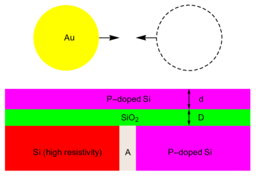
We imagine that the sphere can be moved in a plane parallel to the surface of the patterned plate, from a position (represented by the filled yellow disk in Fig. 1) to the position (represented by the dashed empty disk in Fig. 1). We shall denote as and the respective Casimir forces on the sphere. It is assumed that the vertical projections of the points and lie deep into the left and right sectors of the plate, respectively bimoiso3 . This ensures that in the computation of the forces and one can neglect the sharp boundary separating the left and the right halves of the plate, and treat both sectors as infinitely wide in all directions in the horizontal plane. The quantity of interest to us is the differential force :
| (1) |
For separations , the force can be estimated using the proximity force approximation (PFA) book2 . It has been recently shown that the error implied by PFA in the sphere-plate force is smaller than jaffe ; apl ; teo ; bimoprec ; gert . For our configuration, the PFA gives:
| (2) | |||
where is Boltzmann constant, are the (imaginary) Matsubara frequencies, is the modulus of the in-plane wave-vector, , and the prime in the summation sign indicates that the term is taken with a weight 1/2. The summation over is taken over the two independent polarizations of the electromagnetic field, i.e. the transverse magnetic (TM) and the transverse electric (TE) modes. To explain the meanings of the reflection coefficients , and that occur in the above Equation, we introduce the following notations. The four materials that constitute our setup, i.e. Au, P-doped Si, and high-resistivity Si shall be distinguished by the labels respectively, and their permittivities shall accordingly be denoted as . The label denotes the vacuum, and we set . Thus denote the Fresnel reflection coefficients for a planar interface between media and :
| (3) | |||||
| (4) |
where . The symbols denote instead the reflection coefficients of a plane-parallel three-layer slab consisting of a thick slab of material covered by two layers made of the materials and , of respective thicknesses and , where is the material of the outer layer. The expression of is:
| (5) |
where
| (6) |
III Three prescriptions for the Casimir force
The Equations presented in the previous Section can be used to compute the differential force, after a specific prescription for the values of the permittivities is made. As it was explained in the Introduction, there exist in the literature three distinct prescriptions for computing the Casimir force between test bodies made of metals and/or conductive doped semiconductors, which for brevity we shall refer to as Drude model, plasma prescription and insulator state prescription (ISP) respectively. Below, we shall discuss what they imply for our setup.
III.1 The Drude model
The Drude model represents what we may think of as the “ orthodox” formulation of Lifshitz theory. This formulation, which is based on the fluctuation-dissipation theorem, instructs us to use for the values that correspond to the analytic continuation to the imaginary axis of the “true” complex permittivities of the materials, as can be measured in an optical measurement. As it is well known book2 knowledge of the imaginary part of the permittivity allows to determine via Kramers-Kronig relations, or their generalizations bimonteK ; bimonteKK . Ideally, in a concrete experiment one would measure the optical data of the test bodies that constitute the apparatus. In this work, we shall rely on the tabulated optical data for Au, Si and SiO2 Palik .
In Palik optical data for Au are listed for frequencies larger than eV/. This is not sufficient to compute for small values of (since eV/). Following the standard procedure book2 , the data are extrapolated to low frequencies by a Drude-like model of the form:
| (7) |
where accounts for the contribution of bound (core) electrons, and and are the plasma and the relaxation frequencies, respectively. We set eV/ and eV/ book2 . The Drude model implies:
| (8) |
The Si data of Palik refer to intrinsic (highly resistive) Si, and we shall denote the corresponding permittivity by . For the highly-resistive Si constituting the left sector of our patterned plate we thus set once and for all:
| (9) |
Now we consider P-doped Si. It is known Palik that the permittivity of conductive Si is well described by the formula:
| (10) |
where the Drude term accounts for the contribution of free carriers. The value of is related to the doping concentration by the formula:
| (11) |
where is the electron charge and is the effective electron mass (in P-doped Si the charge carriers are electrons). The value of the relaxation frequency is related, via Eq. (10), to the sample conductivity :
| (12) |
We shall fix rad/sec, which represents the value of the relaxation frequency for a concentration (close to the critical value for P-doped Si ). The chosen value of corresponds to the conductivity silic . We remark that the precise value of is not important for our purposes, because the force is only weakly dependent on . The Drude model implies that for the conductive Si constituting both the over-layer and the right sector of our plate we should set:
| (13) |
Finally, we consider SiO2. This is an insulator. In our computations we fix once and for all:
| (14) |
where for we take the data in Palik .
It is interesting to note that within the Drude model, the reflection coefficients , and attain a universal value for vanishing frequency, i.e. for the Matsubara index that corresponds to the so-called classical term of Lifshitz formula. It is a simple matter to check that:
| (15) |
| (16) |
According to Eq. (II) this implies that the classical term contributes nothing to within the Drude model.
III.2 The plasma prescription
As we discussed in the Introduction, thermodynamic considerations based on the Nernst theorem together with the results of several precise experiments motivated some investigators to propose a new prescription book2 for computing the Casimir force between metallic and/or semiconducting bodies. This alternative prescription, that we shall refer to as the plasma prescription, posits the following rule book2 ; RMP :
plasma prescription: if a conductor is in the conducting state (i.e. is a conductor at ) the contribution of its free carriers must be included in the computation of the Casimir force, but relaxation phenomena must be neglected. In other words, its free carriers should be modeled at low frequency as a dissipation-less plasma.
The implications of the above prescription for the permittivities of the materials that constitute our setup are the following. The values of the Au permittivity should be computed using instead of Eq. (8) the following modified Equation:
| (17) |
Now we turn to conductive Si. As we explained in the Introduction, for carrier concentration a semiconductor is in the conducting state (at ). Thus, the plasma prescription posits that for the permittivity of the conductive Si constituting the over-layer and the right sector of our patterned plate should be computed using the formula
| (18) |
Of course, the permittivities of the highly resistive Si constituting the left sector of the plate, as well as the permittivity of the SiO2 layer are still computed according to Eqs. (9) and (14), respectively. It is interesting to note that the plasma-model reflection coefficients are no more universal in the limit of vanishing frequency. More precisely, while for TM polarization the three zero-frequency reflection coefficients , and remain equal to one, as in the Drude model (see Eq. (15)), the TE reflection coefficients have the following non-universal values:
| (19) |
| (20) |
| (21) |
where we set , . Notice that since , the classical Matsubara term for TE polarization does contribute to the differential force, within the plasma prescription. This fact, which marks an important difference between the plasma and the Drude prescriptions, constitutes the main reason of the different magnitudes predicted by the two prescriptions for the differential force .
III.3 The insulator state prescription
As we explained in the Introduction, thermodynamic considerations suggest to neglect the contribution to the Casimir force of thermally excited carriers in a conducting test body that is an insulator at zero temperature. We thus formulate the following insulator-state prescription (ISP) book2 ; RMP :
insulator-state prescription (ISP): if a conductor is in the insulator state (i.e. is an insulator at ) free charge carriers should be neglected in the computation of the Casimir force.
This prescription applies to P-doped Si, if the carrier concentration is less than the critical density for the Mott-Anderson insulator-metal transition. Thus, according to this prescription the contribution of free charges in the permittivity of conductive Si, represented by the Drude term in Eq. (10), has to be omitted for leaving us with:
| (22) |
This prescription implies that for there is no difference among the permittivities of the highly resistive Si left sector of the plate and of its right conductive Si sector:
| (23) |
This relation implies at once that within the insulator-state prescription the force difference in our setup vanishes for :
| (24) |
We thus see that the insulator-state prescription leads to a sharp prediction: for the measured force difference is zero!
IV Numerical computations
In this Section we present the results of our numerical computations of the force for the setup of Fig. 1. We have considered three different values for the carrier density of the conductive P-doped Si, i.e. , and where is, we recall, the critical density for the Mott-Anderson insulator-metal transition. We note that for the above values of the carrier density, the Debye radius , where is the bare dielectric constant (i.e. not including the carriers contribution) is always much smaller than the separations we shall consider. For example, for the smallest considered density the Debye radius is nm, while the minimum separation that we consider is nm. Since in all cases the influence of spatial dispersion can be safely neglected when considering the contribution of charge carriers to the material response of Si pita , and the local form of Lifshitz theory based on the standard Fresnel reflection coefficients Eqs. (4) is fully adequate.
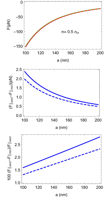
In Fig. 2 we show a plot of the room-temperature Casimir force between a Au sphere and a thick slab of P-doped conductive Si, with a carrier concentration The blue, red and dashed lines in panel 1 correspond to the plasma, Drude and ISP prescription respectively. The second panel displays the difference among the forces which result by including or excluding the contribution of free carriers. The force is computed using either the plasma prescription (solid line) or the Drude prescription (dashed line). The bottom panel shows the magnitude of in percent of the absolute force. The Figure shows that the differences among the forces predicted by the three prescriptions differ by less than 2 pN in the separation region from 100 to 200 nm, representing a change by less than 2.5 percent in the magnitude of the force. It is clear that a discrimination among the three prescriptions based on an absolute force measurement is extremely difficult. Below we show that the differential setup proposed in this work engenders a large amplification of the difference among the three prescriptions.
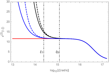
Before we turn to the computation of the differential force, it is useful to make the following observation. According to Lifshitz formula, the Casimir force is expressed by a sum over the Matsubara frequencies . The number of Matsubara frequencies that contribute significantly to the (absolute) Casimir force between two dielectric bodies at distance in vacuum, can be estimated to be around 10 , where is the characteristic frequency of the system. For the minimum separation nm that we are going to consider, this corresponds to something like 120 terms. It is easy to see that far less Matsubara frequencies contribute significantly to the force difference in our setup. This can be understood by looking at Fig. 3, which shows plots of the permittivities along the imaginary axis of intrinsic Si (the red curve) and of conductive P-doped Si for two of the three values of the concentration that we considered, i.e. for (black solid line) and for (blue solid line). The dashed blue and black curves correspond to neglecting in Eq. (10) the relaxation frequency in the Drude term, and so they represent the permittivities that are used to compute the force within the plasma prescription. The dot-dashed vertical left and right lines shown in the Figure correspond, respectively, to the first and to the fifth Matsubara mode, i.e. to and . The Figure clearly shows that the five permittivities are practically undistinguishable for frequencies , and this implies that only the first five or so Matsubara terms, contribute significantly to the force difference . This is very good news for us, because the effect we are after has a low-frequency character, and thus the fact that the differential measurement is insensitive to the uninteresting high-frequency region of the spectrum represents a big plus for the proposed setup. This feature of the apparatus makes it unnecessary to have detailed information on the optical properties of the materials, whose incomplete or inaccurate knowledge represents a source of theoretical uncertainty in absolute force measurements.
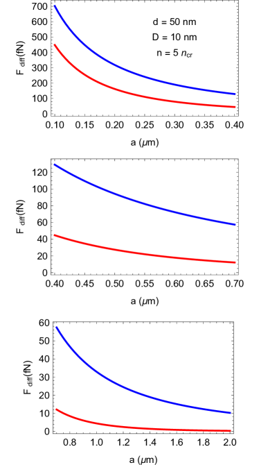
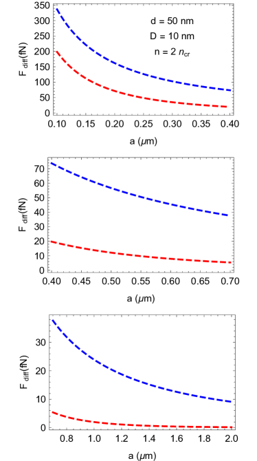
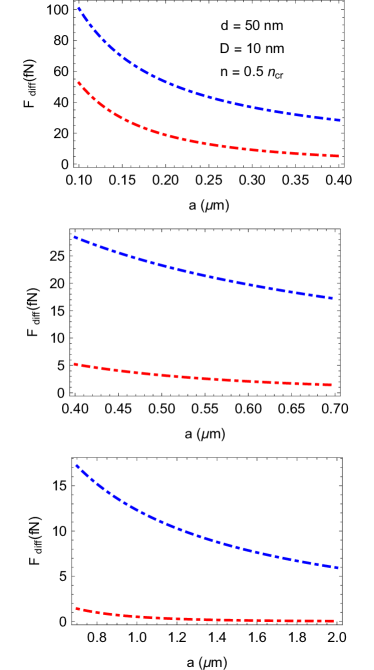
We computed the force for room temperature ( K) in the separation range . Plots of the force (in fN) versus separation are shown in Fig. 4 for , in Fig. 5 for and in Fig. 6 for . In all panels of these three figures, the lower red curves and the upper blue curves correspond to the Drude and plasma prescriptions, respectively. We remark that for the ISP prescription predicts a null force . These figures show that the three prescriptions lead to widely different predictions for the differential force , that should be easily distinguishable in a wide range of separations with an apparatus having a fN sensitivity.
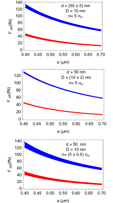
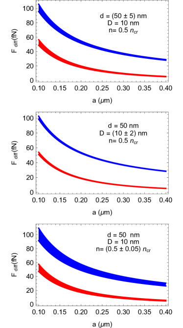
We have checked that the predicted differential force is robust against systematic errors arising from uncertainties in both geometric and material-dependent parameters that characterize our setup. This is demonstrated by Fig. 7 and Fig. 8, which show the bands of variation of the differential force, corresponding to a ten percent uncertainty in the thickness of the conductive Si over-layer (upper panels), in the thickness of the SiO2 layer (middle panels), and in the carrier density (lower panels). In all panels, the lower red bands and the upper blue bands correspond, respectively, to the Drude and plasma prescriptions. Notice that in Fig. 8 no band of variation is displayed for the ISP, since this prescription predicts a null differential force , irrespective of the thickness and , and on the carrier density (provided that remains less than ). The displayed graphs show that the parameter that needs to be better controlled is the concentration of dopant .
Finally, in Fig. 9 we show the band of variation of the differential force corresponding to an uncertainty in the plasma frequency of the gold sphere. The sample variation of the Au plasma frequency has been much debated in the literature (most Casimir experiments use Au test bodies), for it has been shown that an inaccurate determination of this parameter may by itself lead to a large theoretical error, as large as five percent, on the magnitude of the Casimir force vitaly . In order to reduce this source error modified dispersion relations have been devised bimonteK ; bimonteKK that suppress the influence of low frequencies on the determination of the permittivity for imaginary frequencies. It is fortunate that this problem is irrelevant to the present scheme, for the differential force is weakly dependent on the value of . The narrow bands shown in Fig. 9 (in all panels, the lower red bands and the upper blue bands correspond to the Drude and plasma prescriptions respectively) correspond to the wide interval 6.8 eV/ 9 eV/ which includes all sample-dependent values of the plasma frequency that have been reported in the literature vitaly . No band is shown in Fig. 9 for because the differential force is zero within the ISP, independently of the properties of the Au sphere.
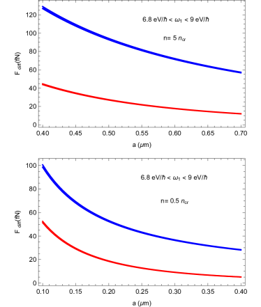
V Conclusions
Over the last 20 years, intense experimental and theoretical investigations of the Casimir effect with conducting test bodies raised puzzling questions about the influence of free charge carriers on the strength of the Casimir force. Theoretical predictions based on Lifshitz theory of dispersion forces between dielectric test bodies appear to be in disagreement with the most precise experiments decca1 ; decca2 ; decca3 ; decca4 ; chang ; bani1 ; bani2 . It appears that in order to bring experimental data into agreement with Lifshitz theory, one has to abandon the natural prescription based on the fluctuation-dissipation theorem of statistical physics, to account for the effect of conductance on the Casimir force. Agreement with data can be achieved by neglecting the effect of relaxation on the free carriers into Lifshitz formula, which means that as far as the Casimir effect is concerned free charges in conducting test bodies behave as a dissipation-less plasma.
Semiconductors offer a unique opportunity to investigate the influence of conduction on the Casimir effect umar2006 ; umar2006bis ; umar1 , since their conductivity can be modified by many orders of magnitude by doping. It has been known for a long time rosen that doped semiconductors undergo a Mott-Anderson metal-insulator transition, when the concentration of dopant atoms exceeds a critical density . It is of great interest to investigate whether the metal-insulator transition has any bearing onto the Casimir effect. The answer to this question depends crucially on the prescription that is used to include the effect of free carriers in doped semiconductors on the Casimir force. According to the standard prescription, based on the fluctuation-dissipation theorem, no effect is to be expected since the optical properties of semiconductors at room temperature do not change appreciably across the transition. A different prescription, based on a thermodynamic argument vladimir , suggests that free carriers contribute to the Casimir force when the semiconductor is in the metallic state, i.e. for doping levels higher than the critical one, while they should be excluded for concentrations less than the critical one. This prescription implies that for the Casimir force a discontinuous change across the metal-insulator transition!
It is clearly of great interest to see if this bold prediction can be tested experimentally. Observation of the effect by conventional Casimir apparatus, based on absolute force measurements, is very hard because the effect is predicted to be small, perhaps one or two percent in the submicron separation range where Casimir experiments are most precise.
In this paper we have described an isoelectronic differential apparatus that should allow for an easy observation of the effect. The crucial ingredient of the setup is a micro-fabricated patterned Si plate, whose left half is made of highly resistive Si, while its right half is made of P-doped Si. A key feature of the patterned plate is the presence of a P-doped thin Si over-layer of uniform thickness, that covers both halves of the plate. The purpose of the over-layer is to screen out possible inhomogeneities in the potential patches that may exist on the surface of the left and right Si slabs, as a result of their different doping levels. The proposed experiment consists in a differential measurement of the force experienced by a Au coated sphere, as it is moved from the undoped left half to the doped right half of the Si plate. The differential character of the measurement ensures automatic cancellation of several effects that plague ordinary Casimir setups, like errors in the sphere-plate separation, roughness, and potential patches. We have also checked that the apparatus is robust against possible uncertainties in the parameters that characterize it, like the thickness of the over-layer, the concentration of dopants, and errors in the optical properties of the materials. In this work we considered for brevity only the case of P-doped Si. Doping the right section of the Si plate by other elements like sulfur vladimir , might lead to a larger differential force and/or a better discrimination among the three theoretical prescriptions for computing the Casimir force. We leave the optimization of the setup for a future work.
In view of the fN sensitivity reached by current differential Casimir apparatus ricardomag ; umardiff , the numerical computations presented in this work show that the proposed scheme should allow for a clear discrimination among alternative theories for the Casimir effect in doped semiconductors. Observation of the effects described in this paper would shed much light on the puzzling and yet unresolved problem of the influence of conductivity on the Casimir effect.
Acknowledgements.
The author thanks G. L. Klimchitskaya and V. M. Mostepanenko for enlightening correspondence during the manuscript preparation, and T. Emig, R. L. Jaffe, N. Graham, M. Kardar and M. Krüger for discussions. .References
- (1) H. B. G. Casimir, Proc. K. Ned. Akad. Wet., 51, 793 (1948).
- (2) K. A. Milton, The Casimir Effect: Physical manifestations of Zero-Point Energy, World Scientific, Singapore (2001).
- (3) V. A. Parsegian, Van der Waals Forces, Cambridge University Press (2005).
- (4) M. Bordag, G. L. Klimchitskaya, U. Mohideen and V. M. Mostepanenko, Advances in the Casimir Effect, Oxford University Press (2009).
- (5) G. L. Klimchitskaya, U. Mohideen, and V. M. Mostepanenko, Rev. Mod. Phys. 81, 1827 (2009).
- (6) A. W. Rodrigues, F. Capasso, and S. G. Johnson, Nature Photonics 5, 211 (2011).
- (7) L. M. Woods, D.A.R. Dalvit, A. Tkatchenko, P. Rodriguez-Lopez, A.W. Rodriguez, and R. Podgornik, Rev. Mod. Phys. 88, 045003 (2016).
- (8) E. M. Lifshitz, Zh. Eksp. Teor. Fiz. 29, 94 (1955) [Sov. Phys. JETP 2, 73 (1956)].
- (9) S.M. Rytov, Theory of Electrical Fluctuations and Thermal Radiation, Publyshing House, Academy os Sciences, USSR (1953).
- (10) G. Bimonte, T. Emig, M. Kardar, and M. Krüger, Ann. Rev. Cond. Matt. Phys. 8, 119 (2017).
- (11) P. J. van Zwol, G. Palasantzas, and J. Th. M. De Hosson, Phys. Rev. B 77, 075412 (2008).
- (12) W. J. Kim, M. Brown-Hayes, D. A. R. Dalvit, J. H. Brownell, and R. Onofrio Phys. Rev. A 78, 020101(R) (2008).
- (13) S. de Man, K. Heeck, and D. Iannuzzi Phys. Rev. A 79, 024102 (2009).
- (14) C. C. Speake and C. Trenkel, Phys. Rev. Lett. 90, 160403 (2003).
- (15) R. O. Behunin, D. A. R. Dalvit, R. S. Decca, C. Genet, I. W. Jung, A. Lambrecht, A. Liscio, D. López, S. Reynaud, G. Schnoering, G. Voisin, and Y. Zeng, Phys. Rev. A 90, 062115 (2014).
- (16) .I Pirozhenko, A. Lambrecht, and V. B. Svetovoy, New. J. Phys. 8 238 (2006).
- (17) G. Bimonte, Phys. Rev. A 81 062501, (2010).
- (18) G. Bimonte, Phys. Rev. A 83, 042109 (2011).
- (19) R. S. Decca, E. Fischbach, G. L. Klimchitskaya, D. E. Krause, D. López, and V. M. Mostepanenko, Phys. Rev. D 68, 116003 (2003).
- (20) R. S. Decca, D. López, E. Fischbach, G. L. Klimchitskaya, D. E. Krause, and V. M. Mostepanenko, Ann. Phys. (N.Y.) 318, 37 (2005).
- (21) R. S. Decca, D. López, E. Fischbach, G. L. Klimchitskaya, D. E. Krause, and V. M. Mostepanenko, Phys. Rev. D 75, 077101 (2007).
- (22) R. S. Decca, D. López, E. Fischbach, G. L. Klimchitskaya, D. E. Krause, and V. M. Mostepanenko, Eur. Phys. J. C 51, 963 (2007).
- (23) C.-C. Chang, A. A. Banishev, R. Castillo-Garza, G. L. Klimchitskaya, V. M. Mostepanenko, and U. Mohideen, Phys. Rev. B 85, 165443 (2012).
- (24) A. A. Banishev, G. L. Klimchitskaya, V. M. Mostepanenko, and U. Mohideen, Phys. Rev. Lett. 110, 137401 (2013).
- (25) A. A. Banishev, G. L. Klimchitskaya, V. M. Mostepanenko, and U. Mohideen, Phys. Rev. B 88, 155410 (2013).
- (26) A. O. Sushkov, W. J. Kim, D. A. R. Dalvit, and S. K. Lamoreaux, Nature Phys. 7, 230 (2011).
- (27) V. B. Bezerra, G. L. Klimchitskaya, and V. M. Mostepanenko, Phys. Rev. A 65, 052113 (2002).
- (28) V. B. Bezerra, G. L. Klimchitskaya, and V. M. Mostepanenko, Phys. Rev. A 66, 062112 (2002).
- (29) V. B. Bezerra, G. L. Klimchitskaya, V. M. Mostepanenko, and C. Romero, Phys. Rev. A 69, 022119 (2004).
- (30) M. Bordag and I. G. Pirozhenko, Phys. Rev. D 82, 125016 (2010).
- (31) G. Bimonte, Phys. Rev. A 79, 042107 (2009).
- (32) F. Chen, G. L. Klimchitskaya, V. M. Mostepanenko, and U. Mohideen, Phys. Rev. Lett. 97, 170402 (2006).
- (33) F. Chen, U. Mohideen, G. L. Klimchitskaya, and V. M. Mostepanenko, Phys. Rev. A 74, 022103 (2006).
- (34) F. Chen, G. L. Klimchitskaya, V. M. Mostepanenko, and U. Mohideen, Phys. Rev. B 76, 035338 (2007).
- (35) E. Buks and M. L. Roukes, Europhys. Lett. 54, 220 (2001).
- (36) H. B. Chan, V. A. Aksyuk, R. N. Kleiman, D. J. Bishop and F. Capasso, Science 291, 1941 (2001).
- (37) N. W. Ashcroft and N. D. Mermin, Solid State Physics (Harcourt College Publishers, 1976).
- (38) T. F. Rosenbaum, R. F. Milligan, M. A. Paalanen, G. A. Thomas, R. N. Bhatt, and W. Lin, Phys. Rev. B 27, 7509 (1983).
- (39) Handbook of Optical Constants of Solids, ed. E. D. Palik (Academic, New York, 1985).
- (40) G. L. Klimchitskaya, U. Mohideen, and V. M. Mostepanenko, J. Phys. 24, 424202 (2012).
- (41) B. Geyer, G. L. Klimchitskaya, and V. M. Mostepanenko, Phys. Rev. D 72, 085009 (2005).
- (42) G. L. Klimchitskaya, U. Mohideen, and V. M. Mostepanenko, J. Phys. A: Math. Theor. 41, 432001 (2008).
- (43) B. Geyer, G. L. Klimchitskaya, and V. M. Mostepanenko, Ann. Phys. (N.Y.) 323, 291 (2008).
- (44) G. L. Klimchitskaya and C. C. Korikov, J. Phys.: Condens. Matter 27, 214007 (2015).
- (45) L. P. Pitaevskii, Phys. Rev. Lett. 101, 163202 (2008).
- (46) V. B. Svetovoy, Phys. Rev. Lett. 101, 163603 (2008).
- (47) D. A. R. Dalvit and S. K. Lamoreaux, Phys. Rev. Lett. 101, 163203 (2008).
- (48) B. Geyer, G. L. Klimchitskaya, U. Mohideen, and V. M. Mostepanenko Phys. Rev. Lett. 102, 189301 (2009).
- (49) R. S. Decca, E. Fischbach, B. Geyer, G. L.Klimchitskaya, D. E. Krause, D. López, U. Mohideen, and V. M. Mostepanenko, Phys. Rev. Lett. 102, 189303 (2009).
- (50) C.-C. Chang, A. A. Banishev, G. L. Klimchitskaya, V. M. Mostepanenko, and U. Mohideen, Phys. Rev. Lett. 107, 090403 (2011).
- (51) A. A. Banishev, C.-C. Chang, R. Castillo-Garza, G. L. Klimchitskaya, V. M. Mostepanenko, and U. Mohideen, Phys. Rev. B 85, 045436 (2012).
- (52) G. Bimonte, Phys. Rev. Lett. 112, 240401 (2014).
- (53) G. Bimonte, Phys. Rev. Lett. 113, 240405 (2014).
- (54) G. Bimonte, Phys. Rev. B 91, 205443 (2015).
- (55) G. Bimonte, D. López, and R. S. Decca, Phys. Rev. B 93, 184434 (2016).
- (56) R. Castillo-Garza, C.-C. Chang, D. Jimenez, G. L. Klimchitskaya, V. M. Mostepanenko, and U. Mohideen, Phys. Rev. A 75, 062114 (2007).
- (57) R.O. Behunin, D.A.R. Dalvit, R.S.Decca, and C.C. Speake, Phys. Rev. D 89, 051301(R) (2014).
- (58) R. S. Decca, D. López, H. B. Chan, E. Fischbach, D. E. Krause, and C. R. Jamell, Phys. Rev. Lett. 94, 240401 (2005).
- (59) Y.-J. Chen, W. K. Tham, D. E. Krause, D. López, E. Fischbach, and R. S. Decca, Phys. Rev. Lett. 116, 221102 (2016).
- (60) G. Bimonte, G. L. Klimchitskaya, and V. M. Mostepanenko Phys. Rev. A 95, 052508 (2017).
- (61) G. Bimonte, T. Emig, R. L. Jaffe, and M. Kardar, Europhys. Lett. 97, 50001 (2012).
- (62) G. Bimonte, T. Emig, and M. Kardar, Appl. Phys. Lett. 100, 074110 (2012).
- (63) L. P. Teo, Phys. Rev. D 88, 045019 (2013).
- (64) G. Bimonte, Europhys. Lett. 118, 20002 (2017).
- (65) M. Hartmann, G.-L. Ingold, and P. A. Maia Neto, Phys. Rev. Lett. 119, 043901 (2017).
- (66) Quick Reference Manual for Silicon Integrated Circuit Technology, eds. W. E. Beadle, J. C. C. Tsai, and R. D. Plummer (Wiley, New York, 1985).