Gold/Parylene-C/Pentacene Capacitor under Constant-Voltage Stress
Abstract
Degradation of metal-insulator-semiconductor (MIS) capacitors of gold/Parylene-C/Pentacene under constant voltage stress (CVS) was investigated to explore the electrical stability and reliability of Parylene C as a gate dielectric in flexible electronics. A stress voltage of fixed magnitude as high as 20 V, both negative and positive in polarity, was applied to each MIS capacitor at room temperature for a fixed duration as long as 10 s. The CVS effects on the capacitance-voltage curve-shift, the time-dependent leakage current, and the time-dependent dielectric breakdown were measured and analyzed. CVS is observed to induce charge in Parylene-C and its interfaces with gold and Pentacene. The net induced charge is positive and negative for, respectively, negative and positive gate bias polarity during CVS. The magnitude of the charge accumulated following positive gate CVS is significantly higher than that following negative gate bias CVS in the range of 4 to 25 nC cm-2. In contrast, the leakage current during the negative gate stress is three orders of magnitude higher than that during the positive gate stress for the same bias stress magnitude. The charge buildup and leakage current are due to the trapping of electrons and holes near the Parylene-C/Pentacene interface as well as in the Parylene-C layer. Before the application of the CVS, a dielectric breakdown occurs at an electric field of 1.62 MV cm-1. After the application of the CVS, the breakdown voltage decreases and the density of the trapped charges increases as the stress voltage increases in magnitude, with the polarity of the trapped charges opposite to that of the stress voltage. The magnitude and direction of the capacitance-voltage curve-shift depend on the trapping and recombination of electrons and holes in the Parylene-C layer and in the proximity of the Parylene-C/Pentacene interface during CVS.
keywords:
Parylene C, flexible electronics, dielectric polymer, constant-voltage stress, charge buildup.1 Introduction
The stability of flexible devices is a major reliability concern. To enhance environmental stability, passivation/encapsulating layers are used. Another critical reliability concern is device stability against electrical stress. Flexible devices often operate under continuous voltage biases which can affect performance dramatically [1, 2]. The general reason for bias instability is charge trapping [2]; electrode, insulator, and semiconductor interfaces easily trap charges, resulting in device-parameter shifts and degraded performances. Therefore, processes that take place at bimaterial interfaces must be characterized and controlled.
Parylene C is commonly used as a dielectric material for electronic applications [1, 3, 4, 5, 6, 7, 8, 9]. Pinhole-free films of this polymer function well as protection layers[10] to minimize device degradation caused by exposure to air and moisture. In recent years, this polymer has been used for flexible substrates due to its desirable mechanical properties (yield strength of 55.1 MPa and static Young’s modulus of 2.76 GPa) and the ease of deposition in both micrometer- and nanometer-thickness regimes [11]. In addition, we have recently shown that Parylene-C columnar microfibrous thin films are viable candidates for use as interlayer dielectrics [3, 4, 5].
Moreover, Parylene-C thin films exhibit superior electrical insulation characteristics, high breakdown strength (2.5 MVcm-1), and low dielectric loss [11], not only as passivation layers but also as gate dielectrics for organic field-effect transistors (OFETs) [12, 13, 14]. In fact, there is a limited number of materials that can be simultaneously used as a substrate, gate dielectric, and encapsulation layer simultaneously while exhibiting a high-performance level comparable to materials dedicated to a specific application [1, 2].
Parylene-C films have been extensively studied [1, 12, 13, 14, 15, 16, 17, 18, 19, 20] as gate dielectrics in OFETs. However, very little is known about the electrical stability and reliability of Parylene C and its interfaces with the active layers in these devices. Current-voltage measurements are commonly made to study the electrical degradation of OFETs under constant-voltage stress (CVS) [20]. However, capacitance-voltage measurements are more sensitive than current-voltage measurements for investigating interface characteristics [21]. In order to address this shortfall, we investigated the electrical stability and reliability of Parylene C as a gate dielectric using capacitance-voltage measurements.
We undertook a systematic analysis of gold/Parylene-C/Pentacene metal–insulator–semiconductor (MIS) capacitors. In this paper, the effects of CVS, the capacitance-voltage curve-shift, and time-dependent dielectric-breakdown (TDDB) are experimentally analyzed. Needless to add, the gold/Parylene-C/Pentacene system is the heart of the OFET.
2 Experimental Procedures
P-type silicon (-Si) substrates were ultrasonically cleaned in an ultrasonic cleaner (2200 Branson, Emerson, St. Louis, MO, USA) using, successively, acetone, DI water, isopropyl alcohol, and DI water for 10 min each. Subsequently, the cleaned substrates were etched for 20 min using a 1:4 mixture of hydrofluoric acid and DI water.
A 150-nm-thick layer of silicon dioxide (SiO2) was then deposited atop the -Si substrate using a PECVD tool (P-5000, Applied Materials, Santa Clara, CA, USA). Thereafter, a 50-nm-thick adhesion layer of chromium (Cr) was deposited using a sputter tool (Desktop Pro®, Denton Vacuum, Moorestown, NJ, USA). Next, a 150-nm-thick gold (Au) layer was sputtered on top of the Cr layer using the same tool.
Pentacene was purified in gradient-temperature sublimation system (MK-5024-S, Lindberg Electric, Watertown, WI, USA) and then loaded in a tubular chamber. A thermal gradient was maintained along that chamber maintained at about 10-5 Torr pressure. The material was sublimated at 300 ∘C and re-condensed down the tube at 165 ∘C in order to drive out impurities. A 150-nm-thick layer of purified Pentacene was then deposited atop the Au layer via vacuum thermal evaporation (Amod, Angstrom Engineering, Kitchener, ON, Canada) at a rate of 0.2 nm s-1. During that process, the Au/Cr/SiO2/-Si structure was fixed to a rotating chuck and maintained at 0 ∘C in a chamber with a base pressure of Torr.
A 200-nm-thick insulating layer of Parylene C was deposited on top of the Pentacene layer using a physicochemical vapor deposition technique. An aluminum-foil boat loaded with 0.2 g of commercial Parylene-C dimer (980130-C-01LBE, Specialty Coatings and Systems, Indianapolis, IN, USA) was placed inside the vaporizer of a Parylene Labcoater (PDS2010, Specialty Coatings and Systems, Indianapolis, IN, USA). Parylene-C dimer was first vaporized at 175 ∘C and then pyrolyzed into a reactive-monomer vapor at 690 ∘C. The reactive-monomer vapor was diffused onto the Pentacene/Au/Cr/SiO2/-Si structure attached to a rotating platform in a vacuum chamber maintained at 28 mTorr pressure.
Finally, a 150-nm-thick circular disk of Au was sputtered on top of the Parylene-C insulating layer using a shadow mask to form the gate of an Au/Parylene-C/Pentacene capacitor above the Au/Cr/SiO2/-Si bottom structure. The area of the circular disk was set as 7.110-2 cm2.
Capacitance-Voltage (C-V) measurements were carried out using a Precision LCR Meter (HP 4284, Hewlett-Packard, Palo Alto, CA, USA), while the parallel mode of ‘C-D’ option was selected. These measurements were made at 100 kHz frequency and room temperature with an applied gate voltage V and an oscillating voltage signal mV.
Using a Semiconductor Parameter Analyzer (HP 4155C, Hewlett-Packard, Palo Alto, CA, USA), we measured the time-dependent leakage current as a function of time while a stress voltage V was being applied at room temperature. A fresh Au/Parylene-C/Pentacene/Au/Cr/SiO2/-Si structure was used for every value of .
3 Results
3.1 Capacitance-voltage characterizations before CVS
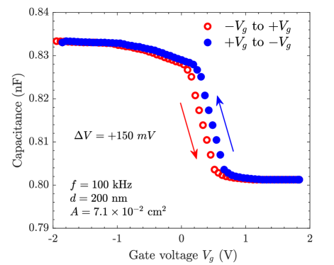
The measured C-V characteristics of an Au/Parylene-C/Pentacene capacitor at 100 kHz are shown in Fig. 1. As this sample was not subjected to CVS, it served as our control sample. Its C-V characteristics were measured in small voltage sweeps from V to V. The capacitance shows an apparent transition from accumulation to depletion. A small hysteresis is evident, the C-V curve-shift of 150 mV being very small [22, 23].
An MIS capacitor is generally modeled as two capacitors in series: the insulator capacitance and the semiconductor-depletion-layer capacitance [21, 22, 24]; hence, the capacitance
| (1) |
For , the measured capacitance reaches a constant value equivalent to given by Eq. 1. In contrast, for , the capacitance saturates to a value close to
| (2) |
where F cm-1 is the permittivity of vacuum. The Parylene-C layer is of thickness nm and the top-electrode area cm2.
3.2 MIS capacitor characterizations under CVS
3.2.1 Capacitance-voltage characterizations after CVS
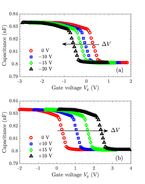
Figure 2 shows the C-V curves measured at 100 kHz in Au/Parylene-C/Pentacene capacitors after the room-temperature application of (a) V and (b) V for duration s. After the 10-s application of , a C-V curve-shift is observed for all three values of , which suggests a positive (resp. negative) charge buildup in the insulator of the MIS capacitor during the application of positive (resp. negative) CVS. For the same and , is higher for than for .
3.2.2 Time-dependent leakage current under CVS
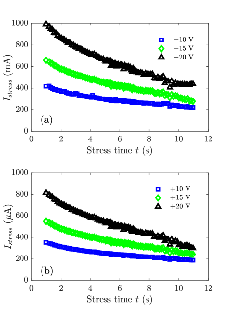
The time-dependent leakage current was measured as a function of s during the application of CVS on MIS capacitors for V. The data presented in Fig. 3 show that is larger for larger . For the same , is lower by three orders of magnitude for than for . Irrespective of the polarity of , decays as increases.
3.2.3 TDDB characterization after CVS
The TDDB characteristics of the Au/Parylene-C/Pentacene capacitors were obtained by recording the current-voltage (I-V) response before and after the 10-s application of . Before CVS, the I-V curve in Fig. 4(a) shows a dielectric breakdown occurs at an electric field of 1.62 MV cm-1. This value is comparable to the values of the breakdown electric field in the range 1.9 to 2.2 MV cm-1 reported for 200-nm-thick Parylene-C layers in MIM structures [9, 25], but for a much smaller gate electrode area of about 310-4 cm2.
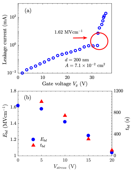
In Fig. 4(b), measured values of the breakdown field and the time-to-breakdown are plotted as functions of V. Time-to-breakdown is the time it takes for the Parylene C to breakdown under the application of each .
As expected, both and decrease as increases. The value of decreases from 1.62 MV cm-1 for the control sample (i.e., ) to 1.04 MV cm-1 for the sample stressed with V. Furthermore, decreases from 1005 s for the control sample to 104 s for the sample stressed with V.
4 Discussion
The C-V characteristics of organic-based MIS capacitors are limited by contact injection [21, 26, 27, 28, 29]. The C-V curve obtained in Fig. 1 can be explained in terms of charge accumulation arising from injection and contained within the semiconductor layer.
For , a thin accumulated layer of injected holes occurs at the Au/Pentacene interface, while the Parylene-C/Pentacene interface is depleted and devoid of any significant free charge carriers. As a result, a depletion layer is created inside the Pentacene. Hence, the capacitance is given by in Eq. 1. For , an accumulation of holes occurs near the interface of Pentacene/Parylene-C. As further increases to more negative values, increases and approaches given by Eq. 2.
The C-V curve shifts observed in Fig. 2 are attributed to charge buildup in Parylene C [30, 31]. Charges of three different provenances are associated with [30, 31]; i.e.,
| (3) |
Here, is the charge density of mobile positive charges located in the bulk of the insulator and arising from ionic impurities such as Na+. The effect of these charges can be seen as a hysteresis in the C-V curve when sweeping in a negative-positive-negative loop. Also, is the charge density of charges trapped in the bulk insulator. It can be either negative or positive, depending on whether holes or electrons are trapped. is the charge density of charges trapped in the semiconductor/insulator interface. It can also be either negative or positive. Because these charges are trapped at the interface, has the largest effect on .
As can be deduced from Fig. 1, is negligibly small because a very small hysteresis ( mV) is detected as the gate voltage is swept from V to V to V. Hence, plays no role in the charge buildup observed in Parylene C after the application of CVS so that
| (4) |
Let us now attempt a quantitative analysis of and its dependence on and . Accordingly [32],
| (5) |
Table 1 provides the values of for V. Clearly, the charge buildup are positive for but negative for . Furthermore, for fixed , the charge buildup is more than twice in magnitude for than for .
| (V) | |||||||
| +10 | +15 | +20 | |||||
| (V) | +0.76 | +1.37 | +2.10 | ||||
| (C cm | +4.10 | +6.50 | +1.04 | ||||
During the time that , electrons are injected from the gate and holes are injected from the layer of accumulated holes near the Parylene-C/Pentacene interface. Electrons and holes transiting the Parylene-C layer can be trapped at defect sites and give rise to charge buildup. It is apparent from Table. 1 that hole trapping dominates and the net charge buildup is positive for .
In contrast and during the time that , holes are only injected from the gate into Parylene-C. The resulting hole-leakage current is observed to be much smaller than shown in Fig. 3(a). This is because a significant portion of the applied is dropped across the depleted (i.e., devoid of charge carriers) layer near the Pentacene/Parylene C interface; much less hole transport takes place across Pentacene for . However, the charge-buildup sign is negative, which may indicate that the observed charge buildup is not entirely due to the trapping of charge carriers (electrons and holes) but could also be caused by defect generation. Presumably, these generated defects are electrons traps that are populated during the application of .
The I-V curve in Fig. 4(a) shows a dielectric breakdown occurs at an electric field of 1.62 MV cm-1. This breakdown may indicate the formation of a defect-related conduction path [33, 34]. In other words, a higher applied voltage could induce defects that eventually form different conducting paths from the gate to the semiconductor in the Au/Parylene-C/Pentacene structure.
As shown in Fig. 4(b), the decrease in suggests that more/longer conductive paths are formed with increasing . Conductive paths result from defect-generation processes and, hence, more defects are presumably generated as further increases to higher values. This deduction is in agreement with earlier inference from Table 1 that defect generation dominates over charge trapping during .
5 Concluding Remarks
A systematic analysis of the reliability of Au/Parylene-C/Pentacene MIS capacitors under constant-voltage stress was performed, with focus on the effects of CVS on the stability of Parylene C as a gate dielectric. 200-nm-thick Parylene-C thin films were utilized as gate-dielectric layers of Au/Parylene-C/Pentacene MIS capacitors. Measurements and analysis of the C-V curve-shift, the time-dependent leakage current, and the time-dependent dielectric breakdown were performed before and after application of CVS. Positive and negative stress voltages of the same magnitude were applied for 10-s duration.
A summary of our results is as follows:
-
1.
The MIS capacitance shows an apparent transition from accumulation to depletion.
-
2.
The C-V curve-shift is higher for positive stress voltage than for negative stress voltage of the same magnitude.
-
3.
The time-dependent leakage current for positive stress voltage is three orders of magnitude lower than for negative stress voltage.
-
4.
The charge density of trapped charges increases with the stress voltage, the polarity of the trapped charges being opposite to the polarity of the stress voltage.
-
5.
As the application of CVS increases, the breakdown voltage decreases as does the time to breakdown.
Therefore, our main conclusions are as follows:
-
1.
The C-V characteristic can be explained in term of accumulation charges within the semiconductor layer.
-
2.
This accumulation charge is due to contact injection.
-
3.
Inside the insulating layer,the charge buildup resulting from the accumulation of trapped charges affects the stability of the the MIS capacitor by shifting its C-V curve.
-
4.
The shift of the C-V curve is attributed to the trapping and recombination of electrons and holes inside Parylene C and its interface with Pentacene.
-
5.
The dielectric-breakdown mechanism is defect dominated.
Overall, the buildup of trapped charges in the Parylene-C layer and near the Parylene-C/Pentacene interface plays a major role in the degradation of Au/Parylene-C/Pentacene capacitors. Our analysis in this paper provides a first-level understanding of the charge buildup in Au/Parylene-C/Pentacene capacitors and, perhaps, will serve as the basis of future studies on the defect-generation process and the trapping of charge carriers within the insulator layer in OFETs.
Acknowledgment
We thank Prof. Chris Giebink for providing access to the vacuum thermal evaporation tool in the Applied Optoelectronics & Photonics Lab at the Pennsylvania State University. AL is grateful to the Charles Godfrey Binder Endowment at the Pennsylvania State University for ongoing support of his research activities.
References
References
- [1] T. Marszalek, M. Gazicki-Lipman, and J. Ulanski, Beilstein J. Nanotechnol. 8, 1532 (2017).
- [2] W.H. Lee, H.H. Choi, D.H. Kim, and K. Cho, Adv. Mater. 26, 1634 (2014).
- [3] I.H. Khawaji, C. Chindam, O.O. Awadelkarim, and A. Lakhtakia, IEEE Trans. Electron Dev. 64, 3360 (2017).
- [4] I.H. Khawaji, C. Chindam, O.O. Awadelkarim, and A. Lakhtakia, Flex. Printed Electron. 2, 045012 (2017).
- [5] I. H. Khawaji, O. O. Awadelkarim, and A. Lakhtakia, IEEE Trans. Dielectr. Electr. Insul. 26, 270 (2019).
- [6] C. Chindam, N.M. Wonderling, A. Lakhtakia, O.O. Awadelkarim, and W. Orfali, Appl. Surf. Sci. 345, 145 (2015).
- [7] C. Chindam, A. Lakhtakia, O.O. Awadelkarim, and W. Orfali, J. Appl. Phys 116, 134905 (2014).
- [8] J.-M. Hsu, L. Rieth, R.A. Normann, P. Tathireddy, and F. Solzbacher, IEEE Trans. Biomed. Eng. 56, 23 (2009).
- [9] E.-Y. Shin, E.-Y. Choi, and Y.-Y. Noh, Org. Electron. 46, 14 (2017).
- [10] X. Xie, L. Rieth, L. Williams, S. Negi, R. Bhandari, R. Caldwell, R. Sharma, P. Tathireddy, and F. Solzbacher, J. Neural Eng. 11, 026016 (2014).
- [11] Bulk Parylene C properties: https://scscoatings.com/docs/broch- ures/parylene_properties.pdf (Accessed on 6 December 2018).
- [12] J. Jakabovic̆, J. Kovác̆, M. Weis, D. Has̆ko, R. Srnáek, P. Valent, and R. Resel, Microelectron. J. 40, 595 (2009).
- [13] P. Tewari, R. Rajagopalan, E. Furman, and M.T. Lanagan, J. Colloid Interface Sci. 332, 65 (2009).
- [14] B. Park, K.-J. Im, K. Cho, and S. Kim, Org. Electron. 9, 878 (2008).
- [15] C. Sheraw, D. Gundlach, and T. Jackson, Mater. Res. Soc. Symp. Proc. 558, 403 (1999).
- [16] V. Podzorov, V. M. Pudalov, and M. E. Gershenson, Appl. Phys. Lett. 82, 1739 (2003)
- [17] T. Yasuda, K. Fujita, H. Nakashima, and T. Tsutsui, Jpn J. Appl. Phys. 42, 6614 (2003).
- [18] I. N. Hulea, S. Fratini, H. Xie, C. L. Mulder, N. N. Iossad, G. Rastelli, S. Ciuchi, and A. F. Morpurgo, Nat. Mater. 5, 982 (2006).
- [19] N. Kawasaki, W. L. Kalb, T. Mathis, Y. Kaji, R. Mitsuhashi, H. Okamoto, Y. Sugawara, A. Fujiwara, Y. Kubozono, and B. Batlogg, Appl. Phys. Lett. 96, 113305 (2010).
- [20] K. Fukuda, T. Suzuki, D. Kumaki, and S. Tokito, Phys. Status Solidi A, 209, 2073 (2012).
- [21] A. Nigam, M. Premaratne, and P. R. Nair, Org. Electron. 14, 2902 (2013).
- [22] D.A. Neamen, Semiconductor Physics and Devices: Basic Principles (McGraw–Hill, New York, NY, 2012).
- [23] C.C. Hu, Modern Semiconductor Devices for Integrated Circuits (Prentice–Hall, Upper Saddle River, NJ, 2010).
- [24] W. Wondmagegn, N. Satyala, I. Mejia-Silva, D. Mao, S. Gowrisanker, H. Alshareef, H. Stiegler, M. Quevedo-Lopez, R. Pieper, and B. Gnade, Thin Solid Films 519, 4313 (2011).
- [25] S. Gowrisanker, M. Quevedo-Lopez, H. Alshareef, and B. Gnade, Org. Electron. 10, 1024 (2009).
- [26] A. Nigam, P. R. Nair, M. Premaratne, and V. R. Rao, IEEE Electron Dev. Lett. 35, 581 (2014).
- [27] L. Diao, C. D. Frisbie, D. D. Schroepfer, and P. P. Ruden, J. Appl. Phys. 101, 014510 (2007).
- [28] G. Horowitz, J. Mater. Res. 19, 1946 (2004).
- [29] H. Klauk, Chem. Soc. Rev. 39, 2643 (2010).
- [30] D.K. Schroder, Semiconductor Material and Device Characterization (IEEE Press, Piscataway, NJ, 2006).
- [31] M. Domínguez-Pumar, C.R. Bheesayagari, S. Gorreta, G. López-Rodríguez, I. Martin, E. Blokhina, and J. Pons-Nin, IEEE Trans. Ind. Electron. 64, 3023 (2017).
- [32] D.B. Farmer and R.G. Gordon, J. Appl. Phys. 101, 124503 (2007).
- [33] N. Raghavan, K.L. Pey, and K. Shubhakar, Microelectron. Reliability 54, 847 (2014).
- [34] J. Suñé, G. Mura, and E. Miranda, IEEE Electron Dev. Lett. 21, 167 (2000).