The Sub-band Structure of Atomically Sharp Dopant Profiles in Silicon
The downscaling of silicon-based structures and proto-devices has now reached the single atom scale, representing an important milestone for the development of a silicon-based quantum computer Fuechsle et al. (2012); Weber et al. (2012); Zwanenburg et al. (2013); Watson et al. (2018). One especially notable platform for atomic scale device fabrication is the so-called Si:P -layer, consisting of an ultra dense and sharp layer of dopants within a semiconductor host. Whilst several alternatives exist, phosphorus dopants in silicon have drawn the most interest, and it is on this platform that many quantum proto-devices have been successfully demonstrated Fuechsle et al. (2010); Tettamanzi et al. (2017); Broome et al. (2018); Koch et al. (2019). Motivated by this, both calculations and experiments have been dedicated to understanding the electronic structure of the Si:P -layer platform Carter et al. (2009); Lee et al. (2011); Carter et al. (2011); Drumm et al. (2013); Miwa et al. (2013, 2014); Mazzola et al. (2014a, b). In this work, we use high resolution angle-resolved photoemission spectroscopy (ARPES) to reveal the structure of the electronic states which exist because of the high dopant density of the Si:P -layer. In contrast to published theoretical work, we resolve three distinct bands, the most occupied of which shows a large anisotropy and significant deviation from simple parabolic behaviour. We investigate the possible origins of this fine structure, and conclude that it is primarily a consequence of the dielectric constant being large (ca. double that of bulk Si) Ristic et al. (2004). Incorporating this factor into tight binding calculations leads to a major revision of band structure; specifically, the existence of a third band, the separation of the bands, and the departure from purely parabolic behaviour. This new understanding of the bandstructure has important implications for quantum proto-devices which are built on the Si:P -layer platform.
Si:P -doping offers potential for the realization of true atomic-scale components for quantum computer applications, whilst retaining compatibility with the simple processing, stability and technological relevance of silicon. Understanding, manipulating and controlling the properties of Si:P -layers, has therefore been the centre of an intense research effort, however, a real understanding of the electronic structure has remained elusive. Density functional theory (DFT) calculations and ARPES recently shed new light on these systems, giving the first glimpse of their electronic structure Carter et al. (2009); Drumm et al. (2013); Carter et al. (2013); Miwa et al. (2013): the metallic nature of Si:P -layers was believed to originate from two nearly-parabolic states, called and , dispersing across the Fermi level () as a consequence of the strong electronic confinement created by the P dopants in the semiconducting Si bulk (see Fig. 1(a)). The energy separation of these states, which is called valley-splitting Miwa et al. (2014), together with their many-body interactions Mazzola et al. (2014a) is responsible for transport properties in this material system and ultimately the function of Si:P -layer based quantum electronic devices.
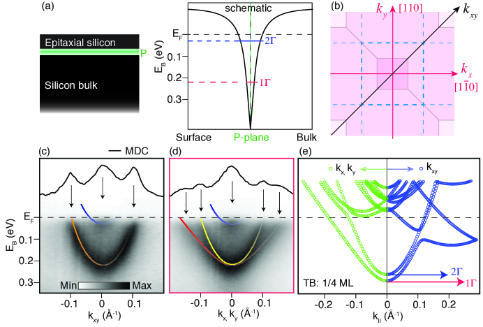
In this work, we show that important details of the electronic bandstructure were previously reported incorrectly. We reveal the presence of additional anisotropic electronic states crossing , resolved only for specific directions in the BZ (see Fig. 1(b)-(d)). Whilst in the diagonal direction () only two electronic states can be seen, along the axial directions ( and ), a clear -band structure is resolved which has not been predicted. The original appears to actually consist of two sub-bands, indicated by the red and yellow parabolae in Fig. 1(d). The presence of three states across cannot be reconciled with published DFT Carter et al. (2009, 2011); Drumm et al. (2013). and tight-binding (TB) calculations Lee et al. (2011). This discrepancy is also seen in our TB calculations (Fig. 1(e) plus details in the Methods section sup ), where only two bands, instead of three, are responsible for the metallic properties of the system. This opens an interesting question about the origin of the sub-band structure resolved by ARPES, as all the states which contribute to this sub-band structure are expected to contribute to the transport properties of Si:P -layers.
We examine some ingredients which have previously been ignored, such as spin orbit coupling (SOC), the role of the dielectric constant, , and an asymmetric doping profile, to explain the origin of this sub-band structure. We show that is dramatically increased in the vicinity of the high density dopant layer, and that this causes additional states originally predicted to be well above (as in Fig. 1(e)) to become occupied.
Before further discussing the origin of the fine structure of Si:P -layers, we first present a qualitative discussion of the electronic structure and the parameters to which it is sensitive. First of all, the available calculations have predicted two nearly parabolic bands with a valley splitting of 30 meV Carter et al. (2009); Lee et al. (2011); Carter et al. (2011); Drumm et al. (2013). It is worth noting that this value is somewhat controversial, and depends on a number of parameters within the model, such as the order/disorder of the dopants Carter et al. (2011). Our measurements reveal the presence of three bands, of which the most occupied bands have a valley splitting which is too small to resolve experimentally (i.e. meV). In other words, the observed valley splitting is either small, or zero. Furthermore, in the axial and directions, the dispersion of the most occupied band deviates significantly from parabolic behaviour, whereas in the diagonal direction (labelled ) the dispersion of these bands is very close to parabolic, and they appear to either be degenerate, or to have a very small separation. The state with its minimum closest to the Fermi level (i.e. the blue parabola in Fig. 1(c,d)) is separated from the other bands by 220 meV, which is very large compared to our TB calculated valley splitting. In other words, it is unclear which of the three bands (if any) correspond to the calculated and . It is especially unclear whether the additional band is split off from , or whether it actually corresponds to the calculated (thereby implying that the least occupied band actually has another origin). In any case, it is clear that the calculated bandstructure deviates significantly from the experimentally observed bandstructure.
In principle, symmetry breaking in one form or another could give rise to additional bands. More specifically, the in-plane dopant order/disorder is not well known in practice, but is thought to influence the electronic structure Carter et al. (2013). In any case, whilst the electronic structure is clearly influenced by the symmetry and ordering of the dopants, this is not able to account for the observed bandstructure sup .
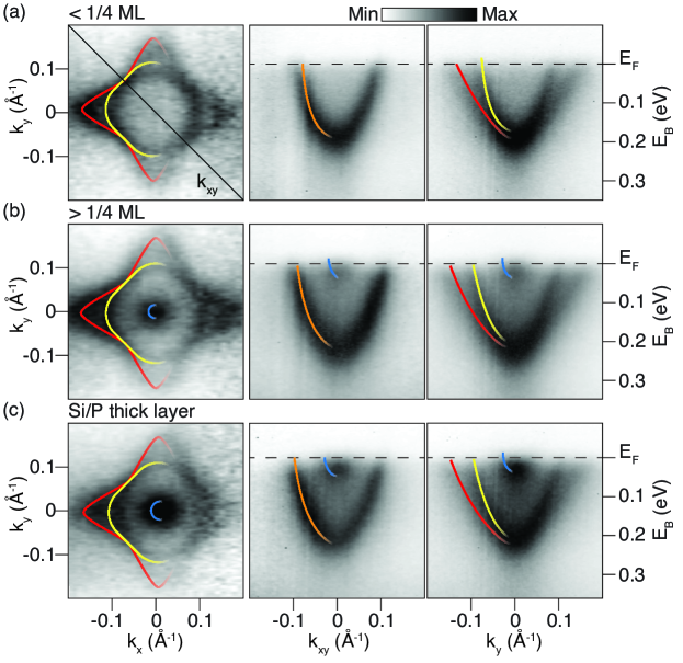
This notion that dopant ordering is not a significant factor is supported empirically: We have prepared three different -layer samples, in which the dopant ordering is dissimilar, however the electronic structure remains very similar. The spectra in Fig. 2(a) correspond to a ‘standard’ single-dose Si:P -layer with of a monolayer (ML) of P dopants in an almost atomically sharp plane. Fig. 2(b) corresponds to a similarly sharp ‘double dose’ with dopant density ML and increased disorder McKibbin et al. (2014). Fig. 2(c) corresponds to a ‘thick’ (1.5 nm) region with a similar (i.e. 25) doping concentration (see Supplementary Material for further details sup ).
The measured band structure is very similar for all three preparations: The electronic structures of Fig. 2 map onto each other very well, needing only a small shift of the bands, to account for the different degrees of doping. Perhaps the most significant difference is that the least occupied band is shifted above the Fermi level when the doping density is lowest. The similarity of the bandstructure for these three different growth methods indicates that dopant ordering cannot be responsible for the mysterious 3rd band.
Symmetry breaking (specifically, the breaking of in-plane inversion symmetry by the dopants in the -layer) together with spin-orbit coupling (SOC) will lift degeneracy and thus give rise to bands which are non-degenerate with respect to their spin Winkler (2003); Rotenberg et al. (1999). This could lead to having two branches, with no splitting at , anisotropic splitting at larger , and a bandstructure which qualitatively matches the ARPES measurements. However, the expected energy splitting due to SOC is about smaller than the observed energy separation of the two most occupied bands sup ; Ferdous et al. (2018a, b). We therefore discount SOC as a possible origin of the observed bandstructure.
The modification of in the vicinity of the -layer is surprisingly important and can significantly influence the electronic structure. For the moderate doping densities found in semiconducting Si wafers, is typically considered to be independent of dopant concentration, but for the extreme doping around the -layer, this view is no longer valid Ristic et al. (2004).
For degenerately doped semiconductors, as the dopant density is increased, a subsequent increase in the susceptibility of the material, and thus in its dielectric constant, can be expected Bethin et al. (1974); Takeshima (1978); Dhar and Marshak (1985). Following the method of Ristić et al. Ristic et al. (2004), it is possible to estimate as a function of dopant density (, in units of cm-3), for phosphorous dopants in Si:
| (1) |
For the case of Si:P -layers, the 2D doping concentration is known to be close to ML. Whilst there is some uncertainty involved in converting the 2D concentration to a 3D concentration, this problem has been addressed previously (see, for example Refs. Polley et al., 2013; McKibbin et al., 2014; Suzuki et al., 2007). Previous works suggest that in the vicinity of the -layer is cm-3 McKibbin et al. (2014); Suzuki et al. (2007), and our own previous work Polley et al. (2013) suggests that whilst the peak concentration is cm-3, we agree that the average concentration within 2-4 nm of the layer is cm-3. Using Eqn. 1, we can therefore estimate that for cm-3, , however at the peak of cm-3 it is conceivable that near to the dopant plane, could be as high as 70. In any case, it is clear that the dielectric constant maybe be several times higher than the value for weakly doped bulk Si.
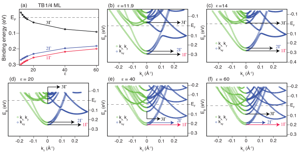
The dependence of the band structure on can be understood in terms of screening: If we consider the -layer as a metal sheet sandwiched within a semiconducting host, then the out-of-plane electric field in the vicinity of the dopant plane will depend on because a larger dielectric constant is associated with more efficient screening. This means that the quantum well is less confined than previously thought (for example, Ref. Lee et al., 2011) and as a result, the splitting between some of the bands is reduced. This qualitative understanding is readily confirmed by TB calculations (see Fig. 3). Interestingly, by increasing the valley-splitting stays roughly constant. However, an additional parabolic band minimum (identified from the calculations as ) is pulled down towards the Fermi level. For , starts to become occupied, and TB calculation looks more similar to the measured bandstructure. As continues to increase, additional parabolic band minima may also be pulled below the Fermi level, and for , a 4th state also becomes partially occupied.
The energy of the , and minima are plotted in Fig. 3(a). By comparison with our experimental data, we find best agreement for : i.e. depending on the preparation, we generally observe the minimum of the most occupied state () to be at meV, and the minimum of the least occupied state (now assigned as ) to be at meV. We also find good agreement with the TB electronic dispersions of Fig. 3(b)-(d); The TB calculation indicates that the two most occupied bands (now assigned as and ) are parabolic, with a small energy separation (30 meV) at =0 and in the diagonal direction, but have an increasing non-parabolic behaviour with increasing in the axial and directions.
Based on ARPES measurements and TB calculations, we conclude that the enhancement of due to the high dopant density is the origin of the additional electronic structure, however, some discrepancies with previous work remain. In previous studies on similar samples Miwa et al. (2014), the 1-2 valley-splitting was reported to be meV, whereas in this work, we conclude that the 1-2 splitting is 30 meV. Due to the lower sample quality and data quality in the earlier work, this was unresolvable and mistaken for a single band, and therefore the previously reported splitting of 130 meV presumably corresponded instead to the 1 (or 2) to 3 splitting. On the other hand, this splitting is still small compared to the TB calculations and ARPES measurements here in which the 2-3 splitting is 200 meV. Whilst it is not possible to give a definitive explanation for this, we propose that it is most likely also a consequence of poorer sample quality; it is known that 1/4 ML dopant activation is only achievable when the Si surface is pristine, and that imperfections act to reduce this number. We therefore consider that the previously reported 130 meV valley splitting presumably corresponds to the (1 or 2) to 3 splitting of a sample with a lower doping concentration that used in the current work.
Finally, we reiterate that a revision of the electronic structure of Si:P is necessary in which three nearly parabolic bands, , and all cross , contrary to only two bands as previously thought. Jointly, all three of these bands must be responsible for the transport properties of the system Polley et al. (2012, 2013) and carrier density. Importantly, the valley-splitting, i.e. separation between and seems to be relatively robust against variations in the sample preparation and can be estimated to be meV. This is an important result which also shows how the properties of a device built upon a Si:P -layer platform are not dramatically affected by changes in the growth, but instead are reliable due to the robustness of the valley-splitting. Indeed, since the valley-splitting in devices built from the Si:P -layer platform affects the lifetime of carriers Hsueh et al. (2014), its correct value and interpretation is important for quantum device performance. Similarly, the presence of a third band crossing will have significant consequences for Si:P -layer based quantum devices, and hence it is important that this is taken into consideration when developing device structures.
Acknowledgements: This work was partly supported by the Research Council of Norway through its Centres of Excellence funding scheme, project number 262633, ‘QuSpin’, and through the Fripro program, project number 250985 ‘FunTopoMat’ the by the VILLUM FONDEN through the Centre of Excellence for Dirac Materials (Grant No. 11744). J. A. M. acknowledges funding support from the Danish Council for Independent Research, Natural Sciences under the Sapere Aude program (Grant No. DFF-6108-00409) and the Aarhus University Research Foundation. P. D. C. K. acknowledges financial support from The Royal Society.
References
- Fuechsle et al. (2012) M. Fuechsle, J. A. Miwa, S. Mahapatra, H. Ryu, S. Lee, O. Warschkow, L. C. L. Hollenberg, G. Klimeck, and M. Y. Simmons, Nat. Nano. 7, 242 (2012).
- Weber et al. (2012) B. Weber, S. Mahapatra, H. Ryu, S. Lee, A. Fuhrer, T. C. G. Reusch, D. L. Thompson, W. C. T. Lee, G. Klimeck, L. C. L. Hollenberg, and M. Y. Simmons, Science 335, 64 (2012).
- Zwanenburg et al. (2013) F. A. Zwanenburg, A. S. Dzurak, A. Morello, M. Y. Simmons, L. C. L. Hollenberg, G. Klimeck, S. Rogge, S. N. Coppersmith, and M. A. Eriksson, Rev. Mod. Phys. 85, 961 (2013).
- Watson et al. (2018) T. F. Watson, S. G. J. Philips, E. Kawakami, D. R. Ward, P. Scarlino, M. Veldhorst, D. E. Savage, M. G. Lagally, M. Friesen, S. N. Coppersmith, M. A. Eriksson, and L. M. K. Vandersypen, Nature 555, 633 EP (2018).
- Fuechsle et al. (2010) M. Fuechsle, S. Mahapatra, F. Zwanenburg, M. Friesen, M. Eriksson, and M. Simmons, Nat Nano 5, 502 (2010).
- Tettamanzi et al. (2017) G. C. Tettamanzi, S. J. Hile, M. G. House, M. Fuechsle, S. Rogge, and M. Y. Simmons, ACS Nano, ACS Nano 11, 2444 (2017).
- Broome et al. (2018) M. A. Broome, S. K. Gorman, M. G. House, S. J. Hile, J. G. Keizer, D. Keith, C. D. Hill, T. F. Watson, W. J. Baker, L. C. L. Hollenberg, and M. Y. Simmons, Nature Communications 9, 980 (2018).
- Koch et al. (2019) M. Koch, J. G. Keizer, P. Pakkiam, D. Keith, M. G. House, E. Peretz, and M. Y. Simmons, Nature Nanotechnology (2019), 10.1038/s41565-018-0338-1.
- Carter et al. (2009) D. J. Carter, O. Warschkow, N. A. Marks, and D. R. McKenzie, Phys. Rev. B 80, 049901 (2009).
- Lee et al. (2011) S. Lee, H. Ryu, H. Campbell, L. C. L. Hollenberg, M. Y. Simmons, and G. Klimeck, Phys. Rev. B 84, 205309 (2011).
- Carter et al. (2011) D. J. Carter, N. A. Marks, O. Warschkow, and D. R. McKenzie, Nanotechnology 22, 065701 (2011).
- Drumm et al. (2013) D. W. Drumm, A. Budi, M. C. Per, S. P. Russo, and L. C. L. Hollenberg, Nanoscale Research Letters 8, 111 (2013).
- Miwa et al. (2013) J. A. Miwa, P. Hofmann, M. Y. Simmons, and J. W. Wells, Phys. Rev. Lett. 110, 136801 (2013).
- Miwa et al. (2014) J. A. Miwa, O. Warschkow, D. J. Carter, N. A. Marks, F. Mazzola, M. Y. Simmons, and J. W. Wells, Nano Letters 14, 1515 (2014).
- Mazzola et al. (2014a) F. Mazzola, M. T. Edmonds, K. Høydalsvik, D. J. Carter, N. A. Marks, B. C. C. Cowie, L. Thomsen, J. Miwa, M. Y. Simmons, and J. W. Wells, ACS Nano, ACS Nano 8, 10223 (2014a).
- Mazzola et al. (2014b) F. Mazzola, C. M. Polley, J. A. Miwa, M. Y. Simmons, and J. W. Wells, Applied Physics Letters 104, 173108 (2014b).
- Ristic et al. (2004) S. Ristic, A. Prijic, and Z. Prijic, Serbian Journal of Electrical Engineering 1, 237 (2004).
- Carter et al. (2013) D. J. Carter, O. Warschkow, N. A. Marks, and D. R. McKenzie, Phys. Rev. B 87, 045204 (2013).
- (19) “See Supplementary Material for details of sample preparation, TB methods, and for calulations of an asymmetric doping profile and siumulations of spin-orbit coupling,” .
- McKibbin et al. (2014) S. R. McKibbin, C. M. Polley, G. Scappucci, J. G. Keizer, and M. Y. Simmons, Applied Physics Letters 104, 123502 (2014).
- Winkler (2003) R. Winkler, Spin-Orbit Coupling Effects in Two-Dimensional Electron and Hole Systems (Springer, 2003).
- Rotenberg et al. (1999) E. Rotenberg, J. W. Chung, and S. D. Kevan, Physical Review Letters 82, 4066 (1999).
- Ferdous et al. (2018a) R. Ferdous, E. Kawakami, P. Scarlino, M. Nowak, D. R. Ward, D. E. Savage, M. G. Lagally, S. N. Coppersmith, M. Friesen, M. A. Eriksson, L. M. K. Vandersypen, and R. Rahman, npj Quantum Information 4, 26 (2018a).
- Ferdous et al. (2018b) R. Ferdous, K. W. Chan, M. Veldhorst, J. C. C. Hwang, C. H. Yang, H. Sahasrabudhe, G. Klimeck, A. Morello, A. S. Dzurak, and R. Rahman, Phys. Rev. B 97, 241401 (2018b).
- Bethin et al. (1974) J. Bethin, T. G. Castner, and N. K. Lee, Solid State Communications 14, 1321 (1974).
- Takeshima (1978) M. Takeshima, Phys. Rev. B 17, 3996 (1978).
- Dhar and Marshak (1985) S. Dhar and A. H. Marshak, Solid-State Electronics 28, 763 (1985).
- Polley et al. (2013) C. M. Polley, W. R. Clarke, J. A. Miwa, G. Scappucci, J. W. Wells, D. L. Jaeger, M. R. Bischof, R. F. Reidy, B. P. Gorman, and M. Simmons, ACS Nano 7, 5499 (2013).
- Suzuki et al. (2007) K. Suzuki, Y. Tada, Y. Kataoka, K. Kawamura, T. Nagayama, S. Nagayama, C. W. Magee, T. H. Buyuklimanli, D. C. Mueller, W. Fichtner, and C. Zechner, IEEE Transactions on Electron Devices, IEEE Transactions on Electron Devices 54, 1985 (2007).
- Polley et al. (2012) C. M. Polley, W. R. Clarke, J. A. Miwa, M. Y. Simmons, and J. W. Wells, Applied Physics Letters 101, 262105 (2012).
- Hsueh et al. (2014) Y.-L. Hsueh, H. Büch, Y. Tan, Y. Wang, L. C. L. Hollenberg, G. Klimeck, M. Y. Simmons, and R. Rahman, Phys. Rev. Lett. 113, 246406 (2014).