Role of Oxygen Adsorption in Nanocrystalline ZnO Interfacial Layers for Polymer–Fullerene Bulk Heterojunction Solar Cells
Abstract
Colloidal zinc oxide (ZnO) nanoparticles are frequently used in the field of organic photovoltaics for the realization of solution-producible, electron-selective interfacial layers. Despite of the widespread use, there is still lack of detailed investigations regarding the impact of structural properties of the ZnO particles, like the particle size and shape on the device performance. In the present work, ZnO nanoparticles with varying surface-area-to-volume ratio were synthesized and implemented into indium tin oxide-free polymer–fullerene bulk heterojunction solar cells featuring a gas-permeable top electrode. By comparing the electrical characteristics before and after encapsulation from the ambient atmosphere, it was found that the internal surface area of the ZnO layer plays a crucial role under conditions where oxygen can penetrate into the solar cells. The adsorption of oxygen species at the nanoparticle surface is believed to cause band bending and electron depletion next to the surface. Both effects result in the formation of a barrier for electron injection and extraction at the ZnO/bulk heterojunction interface and were more pronounced in case of small ZnO nanocrystals with a high surface-area-to-volume ratio. Different transport-related phenomena in the presence of oxygen are discussed in detail, i.e., increasing Ohmic losses, expressed in terms of series resistance, as well as the occurrence of space-charge-limited currents, related to the accumulation of charges in the polymer–fullerene blend. Since absorption of UV light can cause desorption of adsorbed oxygen species, the electrical properties depend also on the illumination conditions. With the help of systematic investigations of the current versus voltage characteristics of solar cells under different air exposure and illumination conditions as well as studies of the photoconductivity of pure ZnO nanoparticle layers, we gain detailed insight into the role of the ZnO nanoparticle surface for the functionality of the organic solar cells.
I Introduction
In polymer-based bulk heterojunction solar cells,Deibel and Dyakonov (2010) the absorber blend, intrinsically, has no preferential transport direction for photogenerated charge carriers due to the statistical intermixing of both the donor and acceptor phase. Therefore, charge-selective interfacial layers,Steim et al. (2010); Ratcliff et al. (2011) which are semipermeable membranes for either electrons or holes in an ideal case,Würfel (2009) are widely applicated to achieve efficient charge extraction at the respective electrodes and determine the device polarity. Amongst the materials for electron collection and transport, ZnO nanoparticles have attracted a lot of attention in polymer photovoltaics,Hau et al. (2008); Huang et al. (2011); You et al. (2013) as they combine the favorable properties of crystalline ZnO (e.g., high electron mobility, wide band gap, n-type conductivity) with the low temperature and solution-based processing methods of colloidal chemistry.Pacholski et al. (2002); Beek et al. (2005) The most critical issue related to thin films made from colloidal nanoparticles is their large internal surface area. This typically results in a high density of surface defects, and the recombination of excess charge carriers at the ZnO/bulk heterojunction interface should be considered as potential loss mechanism in polymer solar cells comprising nanocrystalline ZnO interlayers.Chen et al. (2012); Wu et al. (2013); Shao et al. (2013)
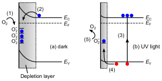
Another well-known feature of ZnO surfaces is the sensitivity to several adsorbates. One prominent example is the chemisorption of ambient oxygen, schematically illustrated in Figure 1. It is generally accepted that chemisorbed oxygen species (e.g., \ceO2 molecules) are able to extract electrons from the conduction band of ZnO (). Consequently, an electron depletion layer forms in the vicinity of the surface, resulting in upward band bending. The vice versa process has been observed under the presence of reducing species, e.g., atomic hydrogen,Li et al. (2012) which would rather lead to electron accumulation and downward band bending at the surface. However, upon illumination with a photon energy above the band gap energy (UV light), electron–hole pairs are created, and photogenerated holes are likely to migrate to the surface and recombine with trapped electrons. Accordingly, the chemisorbed species become discharged and detach from the surface (), resulting in a reduction of the depletion layer width. It is noteworthy that a certain probability for re-adsorption exists, and the resulting adsorption–desorption balance strongly depends on the present oxygen pressure and UV illumination intensity. As being a surface-related phenomenon, the oxygen adsorption–desorption mechanism is particularly pronounced in nanostructures with high surface-area-to-volume ratio, such as nanowires and colloidal nanoparticles, which are, thus, intensively studied for gas sensing,Ghosh et al. (2011); Gurwitz et al. (2014) UV detection,Jin et al. (2008); Dhara and Giri (2011); Guo et al. (2012) and photocatalytic applications.Bora et al. (2013)
Despite the widespread use of ZnO nanoparticles in polymer solar cells, only few publications discuss the influence of ambient oxygen on the electrical characteristics in detail. Lilliedal et al.Lilliedal et al. (2010) investigated flexible roll-to-roll processed devices, comprising a ZnO layer at the bottom electrode. The fabrication was performed in ambient air, and the current versus voltage characteristics of fresh devices exhibited a strong inflection point or S-shaped behavior, which was found to disappear after a certain photo-annealing procedure (i.e., illumination at elevated temperatures). In that context, also a reverse voltage bias treatment ( V) and subsequent light-soaking was discussed.Manor et al. (2012) Recently, Morfa et al.Morfa et al. (2014) studied the UV-enhanced conductivity of nanocrystalline ZnO interlayers in inverted polymer solar cells under consideration of surface photochemistry and regarding the impact of molecular oxygen and water. To date, most literature studies focus on devices with opaque metallic top electrodes, whereas the latter can serve as diffusion barrier for ambient gases. From a more commercial point of view, fully solution-processed polymer solar cells are of great interest, and high-conductivity poly(3,4-ethylenedioxythiophene):poly(styrenesulfonate) (PEDOT:PSS) is frequently used for the realization of printable top electrodes.Gaynor et al. (2010); Zhou et al. (2010) However, polymer films like those made from PEDOT:PSS are known to show a distinct gas permeability,Andersen et al. (2007); Seemann et al. (2009); Norrman et al. (2010); Voroshazi et al. (2011) and, hence, fully solution-processed devices containing ZnO nanoparticles are supposed to be particularly sensitive against ambient oxygen.
In this study, we investigate the influence of the ambient atmosphere on the functionality of nanocrystalline ZnO interfacial layers, which were implemented into inverted poly(3-hexylthiophene) (P3HT):[6,6]-phenyl-C61-butyric acid methyl ester (P3HT:PCBM) bulk heterojunction solar cells in substrate configuration,Glatthaar et al. (2005); Wilken et al. (2012a) comprising an opaque Cr/Al/Cr back contact and a gas-permeable PEDOT:PSS top electrode. Previously, we have reported that the introduction of an interfacial ZnO layer can lead to significantly improved electron extraction at the metallic bottom electrode.Wilken et al. (2012b) Here, we demonstrate that without a suitable encapsulation both the electron injection and extraction at the ZnO/bulk-heterojunction interface are drastically degenerating upon exposure to ambient air on a relatively short time scale and can only partly be recovered using UV containing illumination (light-soaking). By using ZnO nanoparticles with varying surface-area-to-volume ratio, we show that charge injection/extraction is highly sensitive to the internal surface area of the nanocrystalline ZnO film. Depending on the nanoparticle size, different transport-related phenomena are discussed in detail, i.e., Ohmic losses, expressed in terms of an increasing series resistance, as well as the occurrence of space-charge-limited currents, related to the formation of an extraction barrier at the ZnO/bulk-heterojunction interface.
II Experimental Methods
II.1 Synthesis of ZnO Nanoparticles
Zinc oxide nanoparticles were synthesized from zinc acetate dihydrate (\ceZnAc2*2H2O, Sigma Aldrich, 98%) and potassium hydroxide (\ceKOH, Carl Roth, 85%) in methanol, as described in more detail elsewhere.Wilken et al. (2012b); Pacholski et al. (2002) A variation in particle size and shape has been achieved by changing the amount of precursors, while all other synthesis parameters, in particular the ratio between \ceZnAc2*2H2O and \ceKOH, were kept constant. The as-obtained particles were precipitated, washed twice with methanol, and re-dispersed without any additional surfactants with high concentration (50 to 250 mg/ml) in a binary mixture of chloroform and methanol (9:1 v:v). Prior application, stock dispersions were further diluted to yield the desired concentration and filtered through a 0.2 m syringe filter.
II.2 Solar Cell Fabrication
For the inverted solar cells, the bottom contact was thermally evaporated through a shadow mask () on cleaned glass substrates in sequence Cr (6 nm), Al (100 nm), and Cr (12 nm). Subsequently, the ZnO nanoparticles (5 mg/ml) were spin-coated at 1500 rpm in a nitrogen-filled glove box (). Without further treatment of the ZnO layer, a 120 nm thick 1:1 wt:wt absorber blend of P3HT (Merck KGaA, 94.2% regioregularity, Mw = 54 200 g/mol, Mn = 23 600 g/mol) and PCBM (Solenne BV, 99.5%) was then spun from 1,2-dichlorobenzene, slowly dried over about 1 h in a covered petri dish, and afterwards annealed at 150 ∘C. High-conductivity PEDOT:PSS (Heraeus Clevios CPP 105 D) was spin-coated on top of the P3HT:PCBM blend and annealed at 110 ∘C. Finally, a current-collecting Ag grid with a grating period of 1.1 mm was thermally evaporated under high vacuum ( mbar). For encapsulation, devices were sealed with an UV curable optical adhesive (DYMAX Light Weld) and glass slides. The adhesive was cured using a UV lamp (350 nm, 1 mW/cm2). Encapsulation was done in ambient air.
II.3 Characterization Techniques
Structural, morphological, and optical properties of the ZnO nanoparticles were obtained using transmission electron microscopy (Zeiss EM 902A), X-ray diffraction (PANalytical X’PertPro MPD), atomic force microscopy (Agilent 5420), UV-visible absorption (Varian Cary 100), and photoluminescence spectroscopy (Horiba FluoroLog-3). The optical measurements were performed on solutions with low concentration using quartz cuvettes. Background signals resulting from pure solvents were subtracted if necessary. Current density versus voltage characteristics of the inverted solar cells were recorded, under nitrogen atmosphere, with a source-measuring unit (Keithley 2400) and, in ambient air, with a semiconductor characterization system (Keithley 4200). All measurements were performed using four-terminal sensing to avoid the influence of contact and wiring resistances. For illumination, a class AAA solar simulator (Photo Emission Tech.) was used, providing a simulated AM1.5G spectrum. Light intensity was adjusted to 100 mW/cm2 using a calibrated Si reference solar cell. The photoactive area of the solar cells (1 cm2) was delimited by the structured Cr/Al/Cr back electrode. Additionally, we calculated the spectral mismatch factor,Snaith (2012) which was found to be close to unity (1.047) and, therefore, not further taken into account.
II.4 Charge Transport in ZnO Nanoparticle Films
To study the charge transport properties of pure nanocrystalline ZnO films, we implemented them into a lateral metal–semiconductor–metal structure. Therefore, the ZnO nanoparticles were spin-coated on glass and annealed at 150 ∘C for 10 min in a nitrogen-filled glove box. Subsequently, two planar Al electrodes with a thickness of 100 nm and a lateral spacing of 70 m were thermally evaporated under high vacuum ( mbar) on top of the film. Current versus voltage characteristics of the Al/ZnO/Al devices were recorded in the dark and under UV illumination (350 nm, 1 mW/cm2) using a source-measuring unit (Keithley 2400). Measurements were performed both under nitrogen atmosphere and in ambient air.
III Results and Discussion
III.1 Structural and Optical Properties of the ZnO Particles
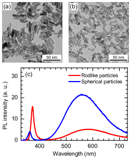
Figures 2a and 2b show transmission electron microscopy (TEM) images of the different types of ZnO nanoparticles discussed in this study, which were obtained using identical synthesis conditions, except the actual precursor concentration. It is well established for the method used that quasi-spherical ZnO nanoparticles can form nanorods by a growth mechanism called oriented attachment, if the precursor concentration is high during synthesis.Pacholski et al. (2002) The particles shown in Figure 2a were prepared with a \ceZnAc2⋅2 H2O concentration of 0.7 mol/l, which yielded nanorods. These particles will be referred to as “rod-like particles” in the following. With a five times lower concentration (0.14 mol/l), the nanoparticles shown in Figure 2b were obtained. In the TEM image, individual quasi-spherical particles as well as short rods, in most cases composed of only two attached ZnO particles, can be observed. For simplicity, the particles of this sample will be called “spherical particles” in the following, although the sample contains also a certain amount of short rods.
Powder X-ray diffraction (XRD) measurements (see Supplemental Material, Figure S1) confirm the formation of wurtzite-type ZnO in both cases, with the spherical particles showing an increased peak broadening due to the smaller diffracting domains. In order to obtain statistical information about the average crystallite size and shape, the measured XRD patterns were modeled by means of Rietveld refinement using the software MAUD,Lutterotti et al. (2004) which can take into account the anisotropic crystallite shape and texture effects. From that analysis, we derived an average crystallite size of nm (rod-like particles) and nm (spherical particles). Thus, in average, the rod-like particles (aspect ratio 3:1) consist of three attached ZnO particles, whereas the other sample (aspect ratio 1.5:1) may be considered as a mixture of spherical particles and short rods, composed of two crystallites. Assuming sphero-capped cylinders, this corresponds to a geometric surface-area-to-volume ratio of 0.51 nm-1 (rod-like particles) and 1.14 nm-1 (spherical particles), respectively.
Figure 2c shows room temperature photoluminescence (PL) spectra of the ZnO nanoparticles excited at 320 nm (3.88 eV). The PL spectra exhibit two emission bands of varying intensity, a characteristic near band-edge emission in the UV, related to band–band transitions, and a broad emission in the visible range, which is often referred to as green luminescence and attributed to trap-assisted recombination. The observed values of the peak wavelength are 373 nm (3.32 eV) and 590 nm (2.2 eV) for the rod-like particles, and 363 nm (3.42 eV) and 565 nm (2.1 eV) for the spherical particles, respectively. Due to quantum confinement, both emission features are blue-shifted in case of the smaller spherical particles relative to the rod-like ones, which is in agreement with the variation of the optical band gap energy from 3.34 eV (rod-like) to 3.43 eV (spherical), as estimated by the absorption onset using the Tauc procedure for direct semiconductors (see Supplemental Material, Figure S2). However, more significant here is the relative intensity between both emission features, and it can be seen that the visible luminescence becomes more pronounced in case of the smaller spherical particles compared to the larger rod-like ones, whereas the opposite trend is obvious for the UV emission band. The corresponding values of the intensity ratio (visible to band edge emission), obtained from integrated peak areas with the abscissa converted to an energy scale, are (rod-like) and (spherical), respectively.
The visible luminescence in ZnO is commonly attributed to recombination of mobile (or shallowly trapped) electrons with deeply trapped holes, and charged oxygen vacancies (V) are often supposed as the corresponding recombination centers.van Dijken et al. (2000); Gong et al. (2007) However, first-principle calculations of the native point defects in ZnO showed that oxygen vacancies are deep donor states with a rather high formation energy, typically resulting in low V concentrations in n-type ZnO.Janotti and de Walle (2007) Instead, zinc vacancies (V) were suggested to be more likely as origin for the visible luminescence, which has also been confirmed experimentally.Tuomisto et al. (2003); Zhao et al. (2005). It could further be shown that the intensity of the visible luminescence increases by the presence of chemisorbed oxygen species, such as and ,Norberg and Gamelin (2005); Ghosh et al. (2011) whereas it is effectively quenched after hydrogen annealingLi et al. (2012); Cooper et al. (2012) or by suitable surface modification with organic molecules.Gong et al. (2007); Norberg and Gamelin (2005) Consequently, it appears reasonable to suggest that the amount of surface states significantly influences the population dynamics of the green luminescence centers (e.g., V), as is also supported by our PL measurements on particles with varying surface-area-to-volume ratio. However, direct recombination via surface states is typically non-radiative, and, hence, the recombination of surface-trapped electrons and holes with their mobile counterparts (which are still existing in the transport bands after photoexcitation) is not likely to explain the increase of the green luminescence with decreasing particle size. One possible explanation has been given in the work of van Dijken et al.van Dijken et al. (2000) Herein, surface-trapped holes in a surface system such as chemisorbed were considered, and the surface-trapped holes have been supposed to tunnel back into the particle where they give rise to the creation of recombination centers for the visible luminescence. The importance of surface hole-trapping was also highlighted in other studies.Li et al. (2012); Teklemichael and McCluskey (2011) Nevertheless, the defect chemistry of ZnO and the origin of the green luminescence are still under debate.Zhang et al. (2010); Gurwitz et al. (2014); Cooper et al. (2012); Djurišić and Leung (2006)
III.2 Solar Cell Characteristics Depending on Atmosphere
To examine the influence of ambient air on the electrical characteristics of polymer–fullerene solar cells containing nanocrystalline ZnO, we implemented thin films made from both types of ZnO particles as electron-selective interfacial layers into indium tin oxide-free inverted devices with the layer sequence Cr/Al/Cr/ZnO/P3HT:PCBM/PEDOT:PSS/Ag grid. High-conductivity grade PEDOT:PSS served as transparent top electrode, whereas a thermally evaporated Ag grid was additionally employed to enhance the lateral conductivity. Details on the device architecture can be found elsewhere.Wilken et al. (2012a, b) The ZnO nanoparticles were applied via spin-coating on the metallic back electrode without any subsequent treatment, and the film thickness was about 20 nm for both the rod-like and spherical particles, as determined by means of spectral ellipsometry (not shown here). We further investigated the surface morphology using atomic force microscopy (see Supplemental Material, Figure S3) and the root-mean-square roughness of films made from the rod-like particles (11.7 nm) is found to be larger as in case of the spherical particles (3.2 nm). This appears reasonable concerning the larger size and the anisotropic shape of the rod-like particles, resulting in a more nonuniform packing in the deposited nanocrystalline films.
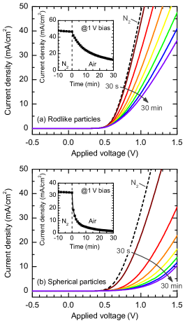
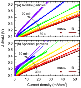
Figure 3 shows dark current density versus voltage (–) characteristics of representative (non-encapsulated) inverted solar cells recorded under different gas environments. After fabrication, the samples were kept under nitrogen atmosphere and the – characteristics initially measured over a period of 10 min. Only negligible changes in the electrical behavior under applied forward bias could be observed during storage under nitrogen, as is visualized by the time development of the current density at a bias voltage of +1 V (insets). Subsequently, the solar cells were transferred to ambient air, and the – characteristics were recorded iteratively between 30 s and 30 min after first contact to air. For both types of nanoparticles, the forward current then exhibits a gradual decrease in magnitude on a relatively short time scale, indicating the degradation of the charge carrier injection and/or transport properties of (at least) one of the electrodes. Apparently, the decay is much faster in case of the smaller, spherically shaped particles. After 30 min of air exposure, a reduction of 73% (95%) in the forward current density (at +1 V bias) can be seen for the rod-like (spherical) nanoparticles compared to the initial state under nitrogen atmosphere. Also changes of the shape of the – curves can be observed upon longer air exposure, especially pronounced for the spherical particles, which further points to a change of the dominant transport mechanism. The latter will be discussed in more detail below. Hence, the different behavior with varying nanoparticle size, whereas all other components of the solar cells were identical, strongly suggest the ZnO/bulk heterojunction interface as origin for the inferior charge carrier injection/transport properties in ambient air.
For an accurate investigation of the electrical characteristics under different illumination conditions, we fabricated a batch of 12 individual solar cells in total, 6 of each comprising interlayers made from the rod-like and the spherical particles, respectively. After fabrication under inert conditions, the devices were transferred to ambient air and kept in dark for a certain time. Subsequently, the – characteristics were measured (i) in the dark, (ii) under AM1.5G illumination with a UV blocking filter (long pass, 400 nm), and (iii) under standard AM1.5G illumination (100 mW/cm2). The samples were then transferred back to the inert atmosphere and annealed at 110 ∘C for 10 min, which was found to entirely recover the initial state. This cycle was performed for three different storage times in ambient air (2, 5, and 10 min) and for each device individually. Afterwards, all devices were encapsulated in ambient air using glass slides and an optically clear adhesive, which was cured using UV illumination. Finally, the – characteristics of the encapsulated devices were recorded under the same illumination conditions as stated before.
| Particles | Encapsulation | (mV) | (mA/cm2) | FF (%) | PCE (%) | (cm2) |
|---|---|---|---|---|---|---|
| rod-like | without (2 min) | 564 4 | 6.5 0.3 | 56.4 1.6 | 2.08 0.12 | 17 1 |
| without (5 min) | 567 3 | 6.5 0.4 | 56.0 2.0 | 2.07 0.14 | 18 2 | |
| without (10 min) | 569 4 | 6.5 0.4 | 54.6 2.7 | 2.01 0.15 | 21 3 | |
| with | 570 6 | 6.4 0.4 | 59.0 2.4 | 2.14 0.13 | 16 1 | |
| spherical | without (2 min) | 563 4 | 6.5 0.3 | 54.0 1.1 | 1.98 0.13 | 21 2 |
| without (5 min) | 567 1 | 6.5 0.2 | 52.2 1.2 | 1.92 0.11 | 24 2 | |
| without (10 min) | 569 4 | 6.3 0.2 | 49.2 1.6 | 1.77 0.10 | 31 2 | |
| with | 570 4 | 6.2 0.2 | 60.8 0.9 | 2.14 0.10 | 16 2 |
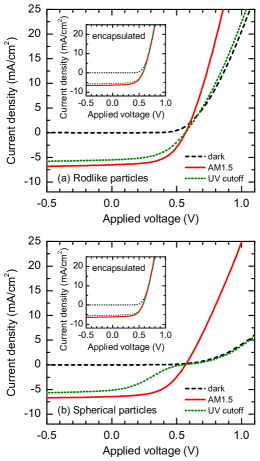
In Figure 4, the – characteristics obtained after 5 min storage in ambient air are shown exemplarily for the devices without encapsulation, as well as after encapsulation (insets). Complete data for all storage times can be found in the Supplemental Material (Figures S4 and S5). The averaged device characteristics, i.e., the open circuit voltage (), the short circuit current density (), the fill factor (FF), the power conversion efficiency (PCE), and the open circuit differential resistance () are summarized in Table 2. From Figure 4, it can clearly be seen that the charge transport under forward voltage bias strongly depends on illumination conditions in case of the non-encapsulated devices. Under standard AM1.5G illumination, the forward current density significantly increases compared to the dark case, whereas it is rather unaffected when the UV part is removed from the illumination source (i.e., when photoexcitation of the ZnO particles is suppressed).
As already shown for the dark case (Figure 3), the effect of ambient air is more pronounced in case of the smaller spherical particles, resulting in an S-shaped – curve under UV-filtered illumination (Figure 4b), whereas the S-shape disappears once the UV filter is removed. However, even in the presence of UV light, the values of the forward current density are lower than those in the initial dark – measurements under nitrogen atmosphere, and the discrepancy increases with time, as is further displayed by the variation of . Consequently, we observed a decrease in FF from 56.4% (54.0%) to 54.6% (49.2%) for the rod-like (spherical) particles after 2 min and 10 min of air exposure, respectively, resulting in a gradual reduction of the PCE from 2.08% (1.98%) to 2.01% (1.77%). Apart from that, relatively slight variations of and are observed, which is probably related to a degradation of the polymer–fullerene blend and is beyond the scope of this study.
In contrast, after encapsulation, the charge injection and transport properties were no longer influenced by the illumination conditions, as is indicated by the identical slope of the – curves in the dark, as well as under UV-filtered and standard AM1.5G illumination (see insets in Figure 4). In that case, no more substantial differences can be seen between solar cells fabricated with the rod-like and spherical particles, respectively, and very similar photovoltaic performances with an FF of and a PCE of have been reached. We also studied the long-term stability of the encapsulated solar cells and found that the beneficial effect of the encapsulation remained for at least several months. For instance, after having been stored in the dark over a period of 10 months, the devices exhibited approximately 95% of their initial PCE (obtained directly after the encapsulation procedure) without any significant change in the charge injection behavior (see Supplemental Material, Figure S6 and Table S1).
III.3 Charge Injection and Extraction at the ZnO/Bulk Heterojunction Interface
First, we discuss whether the decreasing forward current density of non-encapsulated devices upon exposure to ambient air can simply be described by a time-dependent increase of the series resistance . When the forward-biased current density of a diode is dominated by , the inverse slope () of the - curve can be written asHegedus and Shafarman (2004); Schroder (1990)
| (1) |
where is the diode ideality factor, Boltzmann’s constant, the absolute temperature, and the elementary charge. Thus, plotting the quantity versus would yield a straight line with an intercept of and a slope . Figure 5 shows exemplary versus representations of the dark – characteristics under forward bias, depending on the exposure time to ambient air ranging from 0.5 min to 30 min. Furthermore, linear fits of the experimental data according to Equation (1) are shown.
For the rod-like particles, a reasonable fit could be obtained over the whole time range under consideration. This indicates that the degradation of the – curves is mainly related to Ohmic losses and can effectively be described in terms of increasing series resistance. From the slopes of the linear fits, we observed a nearly linear increase in time of , ranging from (0.5 min air exposure) to (30 min air exposure). In contrast, in case of the smaller spherical particles, the versus data show strong deviations from linear scaling, especially pronounced for longer storage in ambient air. Consequently, the degradation of the – curves is unlikely to be attributed to Ohmic losses in that case, and the evaluation of would not lead to meaningful results. Hence, a change of the dominant charge transport mechanism is suggested for the smaller particles in ambient air, which is further consistent with the inferior – performance compared to the larger particles, especially concerning the more pronounced reduction of FF and PCE, and will be addressed in the following.
To study the charge transport properties at the ZnO/bulk heterojunction interface in more detail, we focus now on the – characteristics of the devices under UV-filtered illumination, as shown in Figure 6. The deformation of the – curves in the forth quadrant can clearly be seen after storage in ambient air, in particular, the pronounced S-shape with an inflection point near the voltage axis intercept () in case of the spherical particles. However, the value of is only slightly affected for both types of nanoparticles (), whereas the voltage at the maximum power point () is shifted for non-encapsulated devices by (rod-like particles) and (spherical particles) after 10 min storage in ambient air compared to the ideal case (encapsulated).

An S-shaped deformation of the – characteristics is often observed for organic solar cells with non-ideal contacts.Sandberg et al. (2014); Tress et al. (2011); Wagenpfahl et al. (2010) Recently, Sandberg et al.Sandberg et al. (2014) presented a comprehensive numerical study on several contact-related phenomena and discussed the effect of increased injection barriers, a reduced surface recombination velocity, interfacial minority carrier doping, and charge carrier trapping at the electrodes in detail. They also provide means to experimentally distinguish between the different mechanisms leading to S-shaped - characteristics, and one criterion is the position of the inflection point. According to that analysis, an increasing injection barrier at the ZnO interface is not likely to solely explain the deformation of the – curves in our case, as one would expect a distinct decrease of related to the reduced built-in potential then. Also significant minority carrier doping or interfacial trapping appear unreasonable, as both should lead to an inflection point located well below the voltage axis (), and the forward current would not be decreasing in one of that cases.
In a more favorable manner, our observations can be related to a reduced surface recombination velocity at the ZnO/bulk heterojunction interface, both limiting the current under extraction () and injection () conditions. Based on a numerical device model, Wagenpfahl et al.Wagenpfahl et al. (2010) showed that a reduction of the surface recombination velocity for electrons and holes () gives rise to an inflection point near , which they also confirmed experimentally by modifying the applied indium tin oxide anodes using different oxygen plasma treatments. quantitates the charge extraction for majority charge carriers at each electrode, and a reduction of () points to an extraction barrier for electrons (holes) at the cathode (anode). Extraction barriers could arise due to an insulating layer adjacent to one of the electrodes or a large energetic barrier under charge extraction conditions.Tress and Inganäs (2013) Tress et al.Tress et al. (2011) showed that an extraction barrier for photogenerated charge carriers shifts the onset of the forward current to higher voltages, whereas remains nearly unaffected. This results in the formation of an inflection point near , and is in good agreement with our measurements.
III.4 Unipolar Charge Transport in ZnO Nanoparticle Films
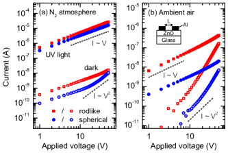
To further investigate the nature of the possible extraction barrier, we studied the unipolar charge transport properties of the ZnO nanoparticle films with respect to the surrounding ambient gas. For that purpose, we processed thin films from both types of ZnO nanoparticles on glass under the same conditions as for solar cell preparation and evaporated two planar Al electrodes on top, separated by a narrow gap (length ). Using that configuration, the conducting channel between the electrodes was in direct contact to the ambient gas, and current versus voltage (–) characteristics of the Al/ZnO/Al devices were recorded (i) under nitrogen atmosphere and (ii) in ambient air. The measurements were performed in the dark and upon exposure to UV illumination (350 nm, 1 mW/cm2), respectively. Figure 7 shows typical - characteristics on a double-logarithmic scale, and the data points are analyzed in terms of power law relations, , where is the scaling exponent. As ZnO/Al contacts are known to be Ohmic,Jin et al. (2008) no corrections have been made for the built-in voltage (). Under nitrogen atmosphere (Figure 7a), we observed for both kinds of nanoparticles a linear scaling of the dark - curve () at lower voltage, indicating Ohmic conduction. This implies that the density of mobile carriers within the nanoparticle films () dominates over the carrier density injected from the contacts (), and the conductivity is given by
| (2) |
where is the charge carrier mobility. At larger bias voltages, a transition to higher scaling exponents can be seen. In case of the smaller spherical particles, the transition is more pronounced, and the scaling exponent reaches a value of , being characteristic for the occurrence of space-charge-limited currents (SCLC). In the SCLC regime, the current is dominated by injected charge carriers (). The current density can then be described by the Mott–Gurney law,
| (3) |
where denotes the relative permittivity, the vacuum permittivity, and the length of a plane-parallel sample.
However, the current increases by several orders of magnitude upon UV illumination, and the photoconduction was found to be Ohmic over the whole range of the applied bias voltage for both types of nanoparticles. From the Ohmic regime, we calculated the conductivity, , where denotes the current density normalized to the contact area, estimated from the product of the film thickness (20 nm) and the contact width (4 mm). From that analysis, we derived a dark conductivity of S/m ( S/m) and a photoconductivity of S/m ( S/m) for the rod-like (spherical) particles, resulting in a photo-to-dark conductivity ratio of (rod-like) and (spherical), respectively.
In contrast, when exposed to ambient air (Figure 7b), the dark – characteristics exhibit strong super-linear behavior even at low voltage, indicating a much lower density of mobile charge carriers compared to inert conditions. At higher voltage, the scaling exponents clearly exceed the limit for trap-free SCLC conduction, which further suggests the presence of deep-level trap states. Upon UV illumination, the – characteristics shift to almost Ohmic conduction, however, the photoconductivity upon air exposure is found to be only S/m ( S/m) for the rod-like (spherical) particles, which is a decrease by two (three) orders of magnitude compared to inert conditions.
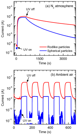
Furthermore, we investigated the transient behavior of the photocurrents by switching on/off the UV illumination, and the results are depicted in Figure 8. After having switched on the illumination, the photocurrent initially increases quickly, followed by a much slower growth process, until saturation has reached. Accordingly, a transient photocurrent decay can be observed when the illumination is switched off, and the decay time strongly depends on the surrounding gas atmosphere. Under nitrogen atmosphere (Figure 8a), the photoconductivity is found to be persistent on the time scale of hours, whereas it decays relatively fast within a few seconds to the dark conductivity level when the sample is exposed to ambient air (Figure 8b). In both cases, the values of the decay time are significantly smaller in case of the smaller spherical particles with the high surface-area-to-volume ratio.
We also studied the spectral photoresponse of the Al/ZnO/Al devices in ambient air (see Supplemental Material, Figure S7). From that analysis, we find that only excitation with photon energies above the band gap energy led to a notable increase of the conductivity compared to dark conditions. This finding indicates that electronic states within the band gap, e.g., populated surface states, have a low optical cross section and is in good agreement with the UV–visible absorption measurements on colloidal solutions.
Our results regarding the transport mechanisms in ZnO nanoparticle films correspond well with the oxygen adsorption–desorption process as described above (Figure 1). Upon air exposure, the ZnO particles are depleted of mobile carriers, leading to strong injection-limited behavior in the dark. During UV illumination, electron-hole pairs are generated and become subsequently separated, as the holes are forced to the surface along the upward band bending, where they are likely to recombine with surface-trapped electrons. At the same time, the recombination probability for the remaining excess electrons in the conduction band decreases, giving rise to the enhanced (Ohmic) photoconductivity. However, the photoconductivity in ambient air is several orders of magnitude lower than that under inert conditions, where the probability for readsorption is dramatically lower.
Regarding the different kind of ZnO nanoparticles used in this study, our results clearly suggest that carrier depletion related to surface adsorption becomes more important with increasing surface-area-to-volume ratio. This is mainly supported by the fact that the electrical properties of the smaller spherical particles are more severely affected by the presence of ambient oxygen compared to the larger rod-like ones, particularly concerning (i) the major difference between the photoconductivity under inert and ambient conditions and (ii) the the faster photocurrent decay after switching off the UV illumination.
III.5 Ambipolar Charge Transport Properties of the Solar Cells
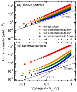
Accordingly, we investigated the ambipolar charge transport properties of the solar cells in more detail. Figure 9 shows log-log representations of the – characteristics under UV cut-off illumination for non-encapsulated devices after different storage in ambient air, as well as for encapsulated devices. Herein, was set to the origin of the voltage axis. For the larger rod-like particles (Figure 9a), it can be seen that the scaling behavior does not depend whether the cell is encapsulated or not. In all cases presented, the scaling exponent obtained via power-law fitting has a value of , which indicates that the dominant charge transport mechanism does not change, at least, during the time scale of the experiment. This further justifies that the degradation of the – curves upon air exposure mainly relates to increasing Ohmic losses at the ZnO/bulk heterojunction interface in case of the rod-like particles with the low surface-area-to-volume ratio, effectively giving rise to the increasing series resistance of the devices.
In contrast, in case of the smaller spherical particles (Figure 9b), the slope of the – curves for the devices without encapsulation is strongly increased compared to the encapsulated devices. Without encapsulation, the scaling exponent increases with longer air exposure from (2 min air exposure) to (10 min air exposure), and, hence, approaches, even exceeds the threshold for SCLC conduction, whereas similar behavior to the case of the rod-like particles is obtained after encapsulation (). In view of this, the S-shaped deformation in ambient air can be interpreted as a transition from an ohmic regime () at low voltages to an SCLC regime () at higher voltages, in agreement with the work of Wagenpfahl et al.Wagenpfahl et al. (2010)
The latter is also consistent with the picture of an effectively reduced surface recombination velocity caused by the formation of a charge extraction barrier. We suppose that the electron depletion in the nanocrystalline ZnO layer and the subsequent upward band bending resulting from the chemisorption of ambient oxygen species lead to an energetic barrier for electron transport and extraction at the ZnO/bulk heterojunction interface. Our findings suggest that the effective height of the energetic barrier correlates with the internal surface area of the nanocrystalline ZnO film. A lower internal surface area (larger rod-like particles) leads to a moderate barrier height, mainly contributing to increased Ohmic losses, whereas, for a higher amount of internal surface area (smaller spherical particles), electron depletion becomes more dominant, leading to an increased extraction barrier. Under extraction conditions (), the higher energetic barrier then results in the accumulation of majority charge carriers in the vicinity of the ZnO interface. Under injection conditions (), also less electrons are injected into the polymer–fullerene blend, leading to a lower bulk recombination rate and, consequently, an accumulation of holes at the anode. Both effects give rise to the formation of space charge and, thus, the transition to SCLC type conduction, causing the S-shape deformation of the – curve. Under the presence of UV light, however, the extraction barrier effectively decreases, as the oxygen desorption becomes favorable over the adsorption process. This finding corresponds well to the beneficial effect of light-soaking, frequently observed for organic solar cells comprising ZnO interfacial layers.Chen et al. (2012); Lilliedal et al. (2010); Manor et al. (2012); Morfa et al. (2014); Cowan et al. (2014)
IV Summary and Conclusions
To summarize the main results, we have studied the impact of the surface-area-to-volume ratio of colloidal ZnO nanoparticles used as electron-selective interlayer in inverted organic solar cells on the electrical properties of the devices. Non-encapsulated devices, where oxygen can penetrate into the solar cells through the gas-permeable PEDOT:PSS top electrode, exhibited fast degradation of the dark current in forward direction on a time scale of minutes, the effect being more pronounced for small ZnO nanocrystals as compared to larger nanorods with a reduced surface-area-to-volume ratio. Under illumination, the injection current strongly increased, but only if the light source contained UV-light which can be absorbed in the ZnO phase. Qualitatively, the decreasing injection current can be explained in terms of oxygen adsorption at the nanoparticle surface which leads to band bending and the formation of a depletion zone at the ZnO surface. For the rod-like particles, the impact of this phenomenon was found to result in an increase of the series resistance of the devices. In contrast, for the smaller particles with a larger specific surface area, the degradation could not be explained simply by Ohmic losses.
Therefore, we had a closer look at the transport properties and determined the photoconductivity of pure ZnO layers. The conductivity under illumination with UV light and in the dark differed by about three orders of magnitude, the difference being again larger for the smaller ZnO nanoparticles. In the dark, exposure to ambient air resulted in the occurrence of space-charge limited currents, but under UV illumination, the transport became of Ohmic nature. Concerning the ambipolar transport in illuminated solar cells, Ohmic behavior was found for solar cells with the larger rod-like particles. In contrast, exposure of non-encapsulated devices with the small nanocrystals led to a transition from Ohmic conduction to an SCLC regime on a time scale of minutes, if the UV part of the spectrum was removed.
From the detailed analysis and systematic variations of air exposure and illumination conditions, we could finally deduce the following scenario: If oxygen can penetrate the devices, adsorption at the ZnO surface leads to a depletion zone and band bending, which in turn results in the formation of a barrier for the injection and extraction of electrons. Under UV illumination, mobile carriers are generated in the ZnO phase, and adsorbed oxygen species can be removed from the surface so that the barrier height is reduced. Since the surface of the ZnO nanoparticles is involved into these mechanisms, it is comprehensible that the effects are more strongly pronounced in the case of smaller nanoparticles with larger surface-area-to-volume ratio. As a finding of this study, we observed in more detail that the specific surface area can be crucial for the nature of charge transport. With the small ZnO nanocrystals, a transition to a space-charge limited regime was observed under air exposure in the absence of UV light. This, in turn, resulted in the formation of an S-shaped – curve under these conditions. In contrast, devices made with the rod-shaped nanoparticles showed a degradation effect as well, but it was much less pronounced, and S-shaped – curves were not obtained, at least on the time scale investigated.
Finally, we have demonstrated that at least in case of using gas-permeable top electrodes like PEDOT:PSS films, light-soaking could only partly recover the initial – behavior of the solar cells obtained directly after fabrication under inert atmosphere. Instead, we highlight the importance of a proper encapsulation of the devices from the ambient atmosphere, not only in order to protect the polymer–fullerene absorber against degradation, but also to preserve the favorable electron extraction capability of nanocrystalline ZnO layers on a long-term scale. With an involved UV curing step, the encapsulation procedure has also been successfully confirmed in ambient air.
Acknowledgements.
The authors thank Janet Neerken, Dorothea Scheunemann, Manuela Schiek, Thomas Madena, and Matthias Macke for valuable support as well as the DYMAX Europe GmbH, Wiesbaden for providing the adhesive used for encapsulation. Funding from the EWE-Nachwuchsgruppe “Dünnschichtphotovoltaik” by the EWE AG, Oldenburg is gratefully acknowledged.References
- Deibel and Dyakonov (2010) C. Deibel and V. Dyakonov, Rep. Prog. Phys. 73, 096401 (2010).
- Steim et al. (2010) R. Steim, F. R. Kogler, and C. J. Brabec, J. Mater. Chem. 20, 2499 (2010).
- Ratcliff et al. (2011) E. L. Ratcliff, B. Zacher, and N. R. Armstrong, J. Phys. Chem. Lett. 2, 1337 (2011).
- Würfel (2009) P. Würfel, Physics of Solar Cells (Wiley-VCH: Weinheim, 2009).
- Hau et al. (2008) S. K. Hau, H.-L. Yip, N. S. Baek, J. Zou, K. O’Malley, and A. K.-Y. Jen, Appl. Phys. Lett. 92, 253301 (2008).
- Huang et al. (2011) J. Huang, Z. Yin, and Q. Zheng, Energy Environ. Sci. 4, 3861 (2011).
- You et al. (2013) J. You, L. Dou, K. Yoshimura, T. Kato, K. Ohya, T. Moriarty, K. Emery, C.-C. Chen, J. Gao, G. Li, and Y. Yang, Nat. Commun. 4, 1446 (2013).
- Pacholski et al. (2002) C. Pacholski, A. Kornowski, and H. Weller, Angew. Chem. Int. Ed. 41, 1188 (2002).
- Beek et al. (2005) W. J. E. Beek, M. M. Wienk, M. Kemerink, X. Yang, and R. A. J. Janssen, J. Phys. Chem. B 109, 9505 (2005).
- Chen et al. (2012) S. Chen, C. E. Small, C. M. Amb, J. Subbiah, T.-h. Lai, S.-W. Tsang, J. R. Manders, J. R. Reynolds, and F. So, Adv. Energy Mater. 2, 1333 (2012).
- Wu et al. (2013) Z. Wu, T. Song, Z. Xia, H. Wei, and B. Sun, Nanotechnology 24, 484012 (2013).
- Shao et al. (2013) S. Shao, K. Zheng, T. Pullerits, and F. Zhang, ACS Appl. Mater. Interfaces 5, 380 (2013).
- Li et al. (2012) M. Li, G. Xing, L. F. N. Ah Qune, G. Xing, T. Wu, C. H. A. Huan, X. Zhang, and T. C. Sum, Phys. Chem. Chem. Phys. 14, 3075 (2012).
- Ghosh et al. (2011) M. Ghosh, R. S. Ningthoujam, R. K. Vatsa, D. Das, V. Nataraju, S. C. Gadkari, S. K. Gupta, and D. Bahadur, J. Appl. Phys. 110, 054309 (2011).
- Gurwitz et al. (2014) R. Gurwitz, R. Cohen, and I. Shalish, J. Appl. Phys. 115, 033701 (2014).
- Jin et al. (2008) Y. Jin, J. Wang, B. Sun, J. C. Blakesley, and N. C. Greenham, Nano Lett. 8, 1649 (2008).
- Dhara and Giri (2011) S. Dhara and P. Giri, Nanoscale Res. Lett. 6, 504 (2011).
- Guo et al. (2012) F. Guo, B. Yang, Y. Yuan, Z. Xiao, Q. Dong, Y. Bi, and J. Huang, Nat. Nanotechnol. 7, 798 (2012).
- Bora et al. (2013) T. Bora, K. K. Lakshman, S. Sarkar, A. Makhal, S. Sardar, S. K. Pal, and J. Dutta, Beilstein J. Nanotechnol. 4, 714 (2013).
- Lilliedal et al. (2010) M. R. Lilliedal, A. J. Medford, M. V. Madsen, K. Norrman, and F. C. Krebs, Sol. Energy Mater. Sol. Cells 94, 2018 (2010).
- Manor et al. (2012) A. Manor, E. A. Katz, T. Tromholt, and F. C. Krebs, Sol. Energy Mater. Sol. Cells 98, 491 (2012).
- Morfa et al. (2014) A. J. Morfa, B. I. MacDonald, J. Subbiah, and J. J. Jasieniak, Sol. Energy Mater. Sol. Cells 124, 211 (2014).
- Gaynor et al. (2010) W. Gaynor, J.-Y. Lee, and P. Peumans, ACS Nano 4, 30 (2010).
- Zhou et al. (2010) Y. Zhou, H. Cheun, S. Choi, W. J. Potscavage, Jr., C. Fuentes-Hernandez, and B. Kippelen, Appl. Phys. Lett. 97, 153304 (2010).
- Andersen et al. (2007) M. Andersen, J. E. Carlé, N. Cruys-Bagger, M. R. Lilliedal, M. A. Hammond, B. Winther-Jensen, and F. C. Krebs, Sol. Energy Mater. Sol. Cells 91, 539 (2007).
- Seemann et al. (2009) A. Seemann, H.-J. Egelhaaf, C. J. Brabec, and J. A. Hauch, Org. Electron. 10, 1424 (2009).
- Norrman et al. (2010) K. Norrman, M. V. Madsen, S. A. Gevorgyan, and F. C. Krebs, J. Am. Chem. Soc. 132, 16883 (2010).
- Voroshazi et al. (2011) E. Voroshazi, B. Verreet, A. Buri, R. Müller, D. D. Nuzzo, and P. Heremans, Org. Electron. 12, 736 (2011).
- Glatthaar et al. (2005) M. Glatthaar, M. Niggemann, B. Zimmermann, P. Lewer, M. Riede, A. Hinsch, and J. Luther, Thin Solid Films 491, 298 (2005).
- Wilken et al. (2012a) S. Wilken, T. Hoffmann, E. von Hauff, H. Borchert, and J. Parisi, Sol. Energy Mater. Sol. Cells 96, 141 (2012a).
- Wilken et al. (2012b) S. Wilken, D. Scheunemann, V. Wilkens, J. Parisi, and H. Borchert, Org. Electron. 13, 2386 (2012b).
- Snaith (2012) H. J. Snaith, Energy Environ. Sci. 5, 6513 (2012).
- Lutterotti et al. (2004) L. Lutterotti, D. Chateigner, S. Ferrari, and J. Ricote, Thin Solid Films 450, 34 (2004).
- van Dijken et al. (2000) A. van Dijken, E. A. Meulenkamp, D. Vanmaekelbergh, and A. Meijerink, J. Lumin. 87–89, 454 (2000).
- Gong et al. (2007) Y. Gong, T. Andelman, G. F. Neumark, S. O’Brien, and I. L. Kuskovsky, Nanoscale Res. Lett. 2, 297 (2007).
- Janotti and de Walle (2007) A. Janotti and C. G. V. de Walle, Phys. Rev. B 76, 165202 (2007).
- Tuomisto et al. (2003) F. Tuomisto, V. Ranki, K. Saarinen, and D. C. Look, Phys. Rev. Lett. 91, 205502 (2003).
- Zhao et al. (2005) Q. X. Zhao, P. Klason, M. Willander, H. M. Zhong, W. Lu, and J. H. Yang, Appl. Phys. Lett. 87, 211912 (2005).
- Norberg and Gamelin (2005) N. S. Norberg and D. R. Gamelin, J. Phys. Chem. B 109, 20810 (2005).
- Cooper et al. (2012) J. K. Cooper, Y. Ling, C. Longo, Y. Li, and J. Z. Zhang, J. Phys. Chem. C 116, 17360 (2012).
- Teklemichael and McCluskey (2011) S. T. Teklemichael and M. D. McCluskey, Nanotechnology 22, 475703 (2011).
- Zhang et al. (2010) L. Zhang, L. Yin, C. Wang, N. Lun, Y. Qi, and D. X. Key, J. Phys. Chem. C 114, 9651 (2010).
- Djurišić and Leung (2006) A. B. Djurišić and Y. H. Leung, Small 2, 944 (2006).
- Hegedus and Shafarman (2004) S. S. Hegedus and W. N. Shafarman, Prog. Photovolt: Res. Appl. 12, 155 (2004).
- Schroder (1990) D. K. Schroder, Semiconductor Material and Device Characterization (Wiley: New York, 1990).
- Sandberg et al. (2014) O. J. Sandberg, M. Nyman, and R. Österbacka, Phys. Rev. Appl. 1, 024003 (2014).
- Tress et al. (2011) W. Tress, K. Leo, and M. Riede, Adv. Funct. Mater. 21, 2140 (2011).
- Wagenpfahl et al. (2010) A. Wagenpfahl, D. Rauh, M. Binder, C. Deibel, and V. Dyakonov, Phys. Rev. B 82, 115306 (2010).
- Tress and Inganäs (2013) W. Tress and O. Inganäs, Sol. Energy Mater. Sol. Cells 117, 599 (2013).
- Cowan et al. (2014) S. R. Cowan, P. Schulz, A. J. Giordano, A. Garcia, B. A. MacLeod, S. R. Marder, A. Kahn, D. S. Ginley, E. L. Ratcliff, and D. C. Olson, Adv. Funct. Mater. 24, 4671 (2014).