A new model for the TCAD simulation of the silicon damage by high fluence proton irradiation
Abstract
For the high-luminosity phase of the Large Hadron Collider (HL-LHC), at the expected position of the innermost pixel detector layer of the CMS and ATLAS experiments, the estimated equivalent neutron fluence after 3000 fb-1 is 21016 neq/cm2, and the IEL (Ionizing Energy Loss) dose in the SiO2 12 MGy. The optimisation of the pixel sensors and the understanding of their performance as a function of fluence and dose makes a radiation damage model for TCAD simulations, which describes the available experimental data, highly desirable. The currently available bulk-damage models are not able to describe simultaneously the measurements of dark current (I-V), capacitance-voltage (C-V) and charge collection efficiency (CCE) of pad diodes for fluences neq/cm2. Therefore, for the development and validation of a new accurate bulk damage model we use I-V, C-V and CCE measurements on pad diodes available within the CMS-HPK campaign and data from samples irradiated recently with 24 GeV/c protons. For the determination of the radiation-induced damage parameters we utilise the ”optimiser” of Synopsys TCAD, which allows the minimisation of the difference between the measured and simulated I-V, C-V and CCE. The outcome of this optimisation, the Hamburg Penta Trap Model (HPTM), provides a consistent and accurate description of the measurements of diodes irradiated with protons in the fluence range from 31014 neq/cm2 to 1.31016 neq/cm2.
I Introduction
Attempts to understand and optimise irradiated silicon sensors using TCAD simulations have been around for quite some time [1, 2, 3, 4, 5]. The biggest challenge for such device simulations is the implementation of a satisfactory model for radiation damage effects. In the attempt to implement a model based on defect spectroscopy, one has to consider that for example, hadron irradiation introduces more than 10 different types of electrically active point and cluster defects in the silicon band-gap. For fluences neq/cm2, microscopic measurements like Thermally Stimulated Current techniques are not possible and for lower fluences only partial information about the defects is available. Furthermore, it is currently not possible to simulate cluster defects in TCAD [6]. Therefore, ”effective models” are developed which assume a minimum number of point defect levels, and tune the parameters to reproduce macroscopic measurements.
II Optimisation
For our study we used 200 m thick float zone p-type diodes with an area of 55 mm2 from the CMS-HPK campaign. The diodes were irradiated at the CERN PS with 24 GeV/c protons to fluences of 0.3, 1, 3, 6, 8 and neq/cm2 and annealed at 60∘C for 80 min. I-V, C-V and CCE measurements with infrared light have been performed at C and C. All simulations have been performed with Synopsys TCAD [7]. For the simulation of the I-V and C-V dependence a 1D model is used. The doping profiles of the and implants are taken from spreading resistance measurements. The bulk doping and the active thickness were adjusted to match the C-V measurements of the non-irradiated diode. As with I-V and C-V measurements alone one cannot obtain a model which describes the CCE from infrared light we used in the optimisation a simulation of the CCE from infrared light at 5 voltage steps. For this, at every voltage a transient simulation over a duration of 15 ns in 2D cylindrical coordinates has been performed. To calculate from this the CCE the simulated transient was corrected for leakage current and integrated over the above mentioned time interval.
For the final optimisation the I-V and C-V at 455 Hz and 1 kHz and the CCE for the fluences 3, 6 and neq/cm2 at C were simultaneously used and the expression
| (1) |
where runs over the different fluences and over the different measurements where and are the simulated and measured quantities, respectively, the minimum and maximum voltage and weighting factors was minimised. The weighting factors can be used to weight the different kind of measurements, but in our case they were usually set to one.
III Results
The final result (see table I) was achieved with an ansatz of 5 traps, where the energy levels and types where taken from microscopic measurements and were fixed for the optimisation. The free parameter for a trap are the introduction rate g, so that the trap concentration is given by Nk = g, and the cross sections , .
| Defect | Type | Energy | gint | ||
|---|---|---|---|---|---|
| [cm-1] | [cm2] | [cm2] | |||
| E30K | Donor | EC-0.1 eV | 0.0497 | 2.300E-14 | 2.920E-16 |
| V3 | Acceptor | EC-0.458 eV | 0.6447 | 2.551E-14 | 1.511E-13 |
| Ip | Acceptor | EC-0.545 eV | 0.4335 | 4.478E-15 | 6.709E-15 |
| H220 | Donor | EV+0.48 eV | 0.5978 | 4.166E-15 | 1.965E-16 |
| CiOi | Donor | EV+0.36 eV | 0.3780 | 3.230E-17 | 2.036E-14 |
In all simulations the impact ionisation model from van Overstraeten - de Man [8] is switched on and for the Ip defect, which is located close to midgap, the trap-assisted tunneling model from Hurkx [9] with a tunnel mass of 0.25 me is used.
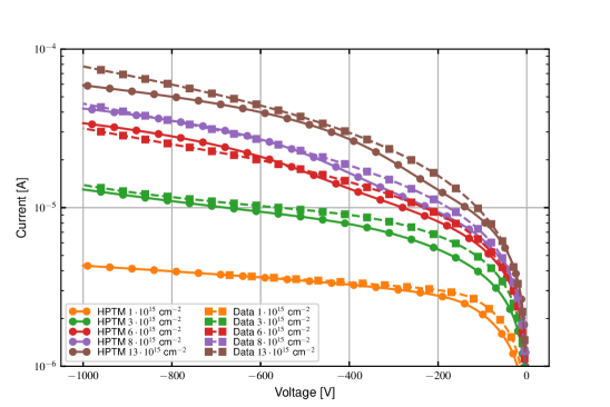
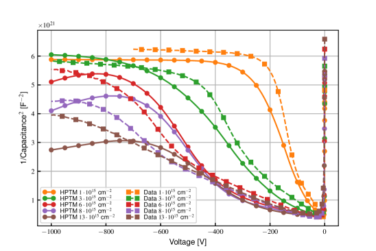
In Fig. 1(a) a comparison of the I-V simulated with the Hamburg Penta Trap Model (HPTM) parameters and the measurements at C for fluences from 1 to neq/cm2 is shown. As can be seen, the simulations reproduce the I-V curves approximately over this fluence range. Similar, in Fig. 1(b) the C-V curves at 455 Hz are shown. For lower voltages the simulation matches the measurements quite well over the full fluence range whereas for the higher voltages and fluences a small deviation is observed. One possible explanation is the onset of impact ionisation at the high voltages.
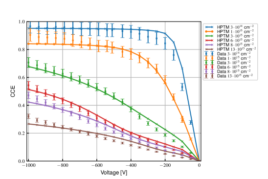
A correct model must describe the voltage dependence of the CCE and reproduce the well know double peak structure of the electrical field [10]. In Fig. 2 the simulations of the CCE for measured signals produced by light from an IR laser at C for the fluences from 0.3 to neq/cm2 are compared to the data. The error bars indicate a 5% systematic uncertainty. A possible dependence of the absorption length on fluence has not been taken into account [11]. As can be seen the simulations reproduce the voltage dependence qualitatively well with the tendency of a slightly too low CCE at high voltages.
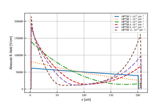
In Fig. 3 the absolute value of the electrical field at -1000 V is shown for the fluences from 0.3 to neq/cm2. The development of the double peak structure with increasing fluence is clearly visible and the peak field of the order of 200 kV/cm requires the usage of impact ionisation in the simulation.
To further validate the HPTM model a comparison of simulated and literature values of measured collected charges [12] of n+-p strip sensors after proton irradiation up to a fluence of neq/cm2 have been performed. The charge collection measurements used 300 m thick AC-coupled strip sensors with a pitch of 80 m and electrons from a 90Sr source. Measurements were done at a temperature of 248 K with an applied reverse bias of 900 V. The strip sensors shown in Fig. 4 with a bulk doping of cm-3 and 5 strips with a pitch of 80 m and an n+-implant width of 18 m were simulated. The AC-coupling was realised with a 250 nm thick SiO2 in combination with a 50 nm thick Si3N4. To evaluate the CCE a Minium Ionizing Particle (MIP) hitting the center of the third strip was simulated using the heavy ion model of Synopsys TCAD and adjusting the generated charge to a value of 80 eh-pairs/m.
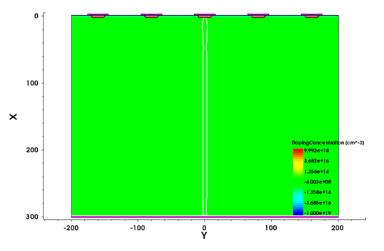
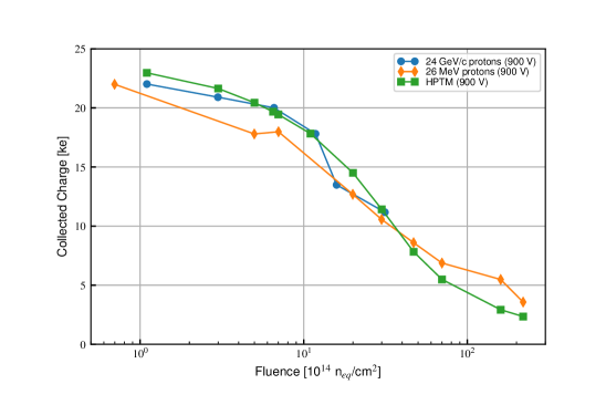
Figure 5 shows the measured collected charge and the collected charge simulated with the HPTM model at a bias voltage of 900 V as function of fluence for n+- p strip sensors irradiated with protons of energies of 26 MeV and 23 GeV. As can be seen a good agreement over the full fluence range is achieved using the HPTM model.
IV Conclusion
In this contribution a radiation damage model with five radiation induced defect states is introduced which gives a significantly better and consistent description of a large set of measurements of pad diodes irradiated with protons in the fluence range from 31014 neq/cm2 to 1.31016 neq/cm2 than previous models [1, 2, 3, 4, 5]. In addition, the application of the HPTM model in the simulation of AC-coupled n+-p strip sensors to model the fluence dependence of proton irradiation gives a good agreement between measurements and simulations.
References
- [1] V. Chiochia, M. Y. Allkofer, D. Bortoletto, L. Cremaldi, S. Cucciarelli, A.Dorokhov, C. Hörmann, D. Kim, M. Konecki, D. Kotlinski, K. Prokofiev, C. Regenfus, T. Rohe, D. A. Sanders, S. Son, and T. Speer, “A double junction model of irradiated silicon pixel sensors for LHC,” Nucl. Instrum. Methods Phys. Res. A, vol. 568, pp. 51–55, 2006.
- [2] M. Petasecca, F. Moscatelli, D. Passeri, and G. U. Pignatel, “Numerical simulation of radiation damage effects in p-type and n-type FZ silicon detectors,” IEEE Trans. Nucl. Sci., vol. 53, no. 5, pp. 2971–2976, Oct. 2006.
- [3] D. Pennicard, G. Pellegrini, C. Fleta, R. Bates, V. O’Shea, C. Parkes, and N. Tartoni, “Simulations of radiation-damaged 3D detectors for the Super-LHC,” Nucl. Instrum. Methods Phys. Res. A, vol. 592, pp. 16–25, 2008.
- [4] T. Peltola, “Simulation of radiation-induced defects,” presented at the 24th International Workshop on Vertex Detectors, Santa Fe, NM, June 1–5, 2015, Paper PoS 031.
- [5] D. Passeri, F. Moscatelli, A. Morozzi, and G.M. Bilei, “Modeling of radiation damage effects in silicon detectors at high fluences HL-LHC with Sentaurus TCAD,” Nucl. Instrum. Methods Phys. Res. A, vol. 824, pp. 443–445, 2016.
- [6] E. Donegani, E. Fretwurst, E. Garutti, R. Klanner, G. Lindstroem, I. Pintilie, R. Radu, and J. Schwandt, “Study of point- and cluster-defects in radiation-damaged silicon,” Nucl. Instrum. Methods Phys. Res. A, vol. 898, pp. 15–23, 2018.
- [7] Synopsys TCAD [Online], Available: http://www.synopsys.com.
- [8] R. van Overstraeten and H. De Man, “Measurement of the Ionization Rates in Diffused Silicon p-n Junctions,” Solid-State Electron., vol. 13, pp. 583–608, 1970.
- [9] G. A. M. Hurkx, D. B. M. Klaassen, and M. P. G. Knuvers, “A New Recombination Model for Device Simulation Including Tunneling,” IEEE Trans. Electron Devices, vol. 39, no. 2, pp. 331–339, Feb. 1992.
- [10] V. Eremin, E. Verbitskaya, and Z. Li, “The origin of double peak electric field distribution in heavily irradiated silicon detectors,” Nucl. Instrum. Methods Phys. Res. A, vol. 476, pp. 556–564, 2002.
- [11] Ch. Scharf, “Radiation damage of highly irradiated silicon sensors,” Ph.D dissertation, Univ. of Hamburg, Hamburg, Germany, 2018.
- [12] A. Affolder, P. Allport, and G. Casse, “Collected charge of planar silicon detectors after pion and proton irradiations up to neq/cm2,” Nucl. Instrum. Methods Phys. Res. A, vol. 623, pp. 177–179, 2010.