1 Introduction
Heat transfer between bodies separated by nanoscale vacuum gap distances has been extensively studied for potential applications in thermal management [Fiorino2018a, Zhu2019], energy conversion [Fiorino2018, Inoue2019, Bhatt2020, Lucchesi2021] and data storage [Albisetti2016]. For vacuum gap distances down to 10 nm, state-of-the-art experiments demonstrated that heat transport is mediated by near-field radiative heat transfer (NFRHT), which can greatly exceed Planck’s blackbody limit [Rousseau2009a, Shen2009, Song2015, St-gelais2016, Bernardi2016, Song2016, Watjen2016, Ghashami2018, Lim2018, Kim2015a, DeSutter2019, Tang2020]. By comparing measurements with theory based on fluctuational electrodynamics [Polder1971, Rytov1989], the tunneling of evanescent electromagnetic waves has been unambiguously identified as the enhancement mechanism. In contrast, phonons become the dominant heat carrier when two objects are brought into contact [Gotsmann2013]. This suggests that there should be a transition between electromagnetic wave-mediated NFRHT and phonon-mediated heat conduction in the near-contact regime.
Various theoretical studies have explored acoustic phonon transport across single-digit nanometer vacuum gaps as a plausible radiation-to-conduction transition mechanism [Sellan2012, Xiong2014, Chiloyan2015b, Alkurdi2020, Prunnila2010, Ezzahri2014, Pendry2016, Wang2017, Sasihithlu2017, Zhang2018, Venkataram2020, Volokitin2020, Chen2021, Tokunaga2021, Tokunaga2022]. These efforts have highlighted the roles of interatomic [Sellan2012, Xiong2014, Chiloyan2015b, Alkurdi2020, Prunnila2010, Ezzahri2014, Pendry2016, Wang2017, Sasihithlu2017, Zhang2018, Venkataram2020, Chen2021, Tokunaga2021, Tokunaga2022] and electrically-driven force interactions [Pendry2016, Volokitin2020, Tokunaga2021] in mediating the so-called acoustic phonon tunneling phenomenon. Only one study experimentally explored acoustic phonon tunneling in the near-contact regime by implementing a scanning tunneling microscope with inelastic electron tunneling spectroscopy for thermal measurement [Altfeder2010]. However, this work employed a simple photon emission model to support the presence of acoustic phonon tunneling and lacks rigorous comparison with measurements. Other studies have probed heat transfer for sub-10-nm vacuum gap distances [Kim2015a, Kittel2005a, Kloppstech2017, Cui2017a], but have not linked heat transfer measurements across both the gap and contact regimes with a unified theoretical model to elucidate the existence of gap-mediated acoustic phonon transport.
This article presents experimental and theoretical results demonstrating that acoustic phonon transport can dominate heat transfer in the near- to asperity contact regimes. To this end, we measure thermal transport from a feedback-controlled platinum (Pt) nanoheater to a flattened silicon (Si) tip in a high-vacuum shear force microscopy (HV-SFM) platform, which can precisely control the tip-nanoheater vacuum gap from single-digit nanometers to bulk contact. By selecting dissimilar materials (Pt and Si), NFRHT is effectively suppressed to make acoustic phonon transport the dominant heat transfer mechanism over the gap range considered[Song2015]. Each of the experimental results are quantitatively compared with calculations based on the atomistic Green’s function (AGF) method for acoustic phonon transport and fluctuational electrodynamics for NFRHT. The theoretical predictions indicate that acoustic phonon transport is driven by the Coulomb force interaction for near-contact vacuum gaps, which gives way to strong interatomic forces at the onset of contact. By analyzing the simultaneously measured tip-nanoheater thermal conductance and lateral force interaction, direct proportionality consistent with the AGF method is revealed and further emphasizes the role of acoustic phonon transport in the experiment. The results indicate acoustic phonon transport as a potential radiation-to-conduction transition mechanism, which can be used to develop active nanoscale thermal management systems.
2 HV-SFM/Nanoheater Experiments
2.1 Experimental setup
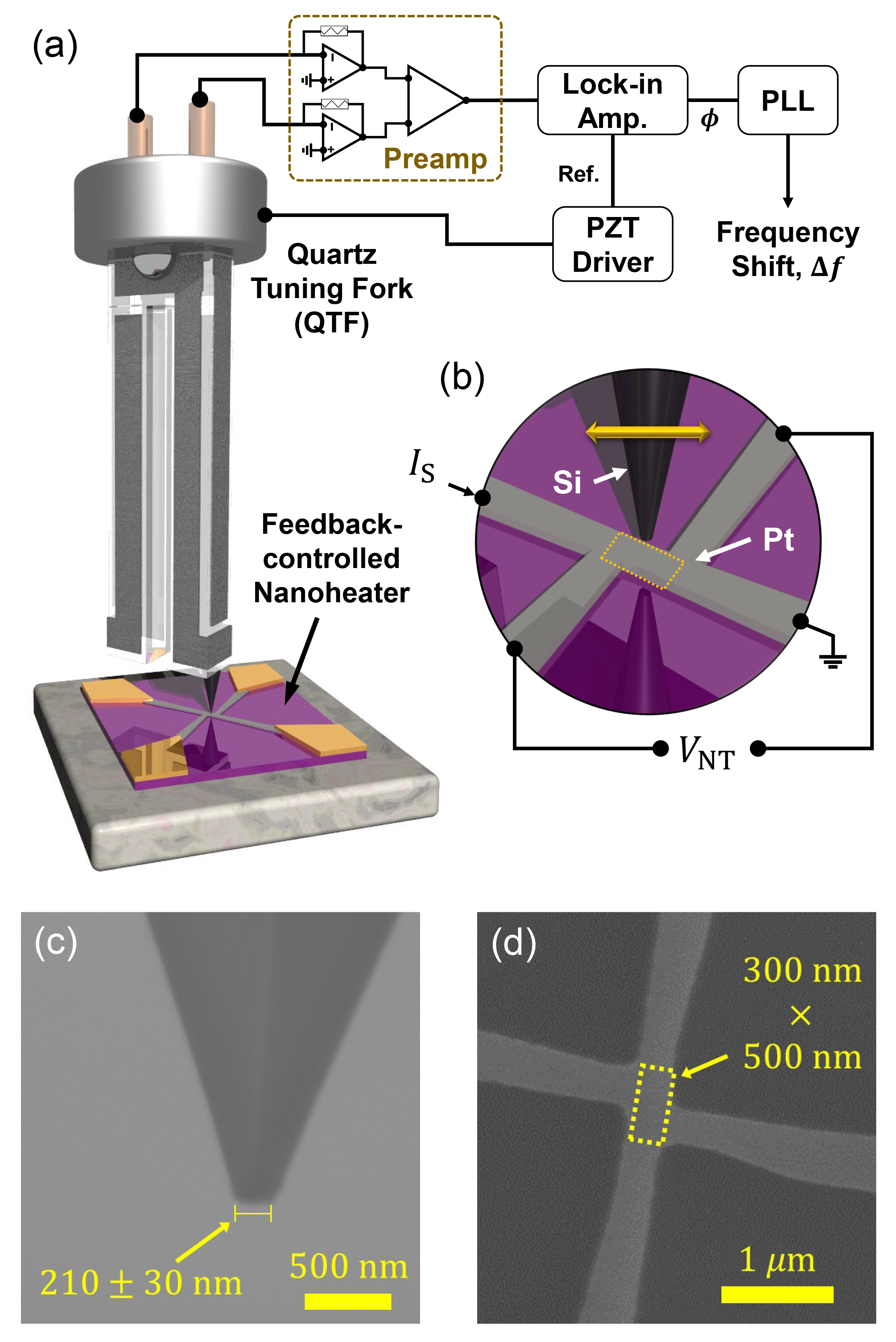
The HV-SFM, shown in Fig. 1(a), is a custom-built, high vacuum system (510-6 Torr in routine operations) that adopts a vertically aligned quartz tuning fork (QTF) probe having an Si tip at the free end of one prong for sensitive tip-sample lateral force measurement. \textcolorredThe HV-SFM is equipped with a piezoelectric sample stage having an x,y,z-scanning range of 30 m 30 m 10 m, respectively, and 16-pin electrical feedthroughs for electric connections during vacuum experiments. The vertical displacement of the sample stage is carefully calibrated to reveal a piezo sensitivity of 28.02.8 nm/V with the position uncertainty of 1.8 Å [SI_Jarzembski], which is precise enough to control the vertical position of the tip with a sub-nanometer resolution.
When mechanically driven at the in-plane, anti-symmetric resonant frequency ( = 32.768 kHz), the QTF probe exhibits a quality factor of 4000 in a high-vacuum environment. This high quality factor allows single-angstrom resolution for tip-sample gap control through monitoring the QTF’s resonance frequency shift (i.e., ) [Karrai2000]. According to the first-order QTF oscillator model, its resonance frequency shift enables quantification of the tip-sample conservative lateral force graidient () using [Castellanos-Gomez2011]. Here, the effective spring constant, , can be approximated as , where is the Young’s modulus of quartz [Grober2000]. Using the dimensions of the QTF prong ( mm; mm; mm), is estimated to be 22.0 kN/m. In addition, the vertically mounted QTF probe enables tip position stability above the sample surface with sub-nanometer gap control, which is not possible in the conventional cantilever-based method due to snap-in contact [Kim2015a]. HV-SFM is also advantageous over the electron tunneling methodologies [Altfeder2010, Kittel2005a, Kloppstech2017, Cui2017a] as the QTF-mounted tip is not necessarily limited to electrically conductive materials. For the present study, an Si tip modified to a flat-top, 210 30 nm in width as shown in Fig. 1(c), is used to secure a sufficiently large heat transfer area as well as to implement a plane-plane configuration for theoretical modeling.
redIn order to minimize any effect of lateral tip motion onto the tip-nanoheater thermal transport measurement, the QTF oscillation amplitude is maintained within the sub-nanometer range. The lateral oscillation amplitude of a QTF probe was measured by optical fiber interferometry (OFI). As illustrated in Fig. S2(a) of the Supplemental Material [SI_Jarzembski], the optical fiber aperture is aligned to the side wall of the tip-attached QTF prong to measure its lateral oscillation amplitude. The lateral oscillation amplitude of the tip () is then estimated from the OFI measurement by using the QTF geometry. Both the electrical outputs from the QTF and OFI are simultaneously demodulated at the QTF resonant frequency to correlate with the QTF electrical signal (). Figure S2(b) of the Supplemental Material [SI_Jarzembski] shows a linear correlation between and , from which the QTF amplitude signal sensitivity is determined to be nm/V. The QTF electrical signal is set to 70 mV-rms at its resonance frequency during experiments, which corresponds to a lateral tip motion of 0.5 nm-rms. This lateral tip motion is on the order of the average lattice constant of the Si-Pt system [Feibelman2001, Esfarjani2011] and is approximately three orders of magnitude smaller than the effective surface area subjected to thermal transport. Such a small lateral tip oscillation does not affect the thermal transport measurement.
The nanoheaters are batch fabricated using e-beam lithography for the nanopatterned Pt strip and photolithography for the micro-patterned gold electrodes [Hamian2016b]. The Pt nanoheater has a sensing region of approximately 300 nm 500 nm between the two inner electrodes, as marked by a yellow dashed box in Figs. 1(b) and (d), allowing a four-point probe electrical resistance measurement. When an electrical current () is supplied to the nanoheater for Joule-heating, the voltage drop () across the inner electrodes is measured to monitor the electrical resistance of the nanoheater’s sensing region (). \textcolorredFor calibration, a nanoheater chip is placed on a heater stage equipped with a temperature controller (Cryo-Con, Model 22C) in the HV-SFM vacuum chamber. The sensing current is set to 100 A to minimize self-heating, while the entire nanoheater chip is bulk-heated in a high vacuum condition [Jarzembski2018]. Figure S3 in the Supplemental Material shows the calibration results of two nanoheaters (nanoheater #1 for the near-contact measurements and nanoheater #2 for the bulk-contact measurements)[SI_Jarzembski], demonstrating that is linearly proportional to the substrate temperature (or the sensing area temperature ). The resultant temperature coefficient of resistance (TCR) is 1.210-3 K-1 for nanoheater #1 and 9.6 10-4 K-1 for nanoheater #2, respectively. Moreover, the sensing region of the nanoheater can be Joule-heated up to 500 K by increasing power dissipation (i.e., ). From the obtained linear correlation between and , the effective thermal resistance of the sensing region () is determined to be 0.533 0.008 K/W for nanoheater #1 and 0.485 0.004 K/W for nanoheater #2. Although the nanoheater TCRs are obtained in the temperature range less than 350 K due to the limit of the heating stage, the linearity measured between and signifies that the obtained TCRs are valid for higher temperatures.
Since the tip side has no sensing component, the nanoheater should measure both the heat transfer rate to the tip () and the sensing region temperature () as the tip approaches the nanoheater. To this end, the electrical current is feedback-controlled to compensate tip-induced thermal transport while is maintained at a set-point value [Jarzembski2018]. \textcolorredFor the optimal response time and noise suppression of the nanoheater, an 8th-order low pass filter with 10 Hz cutoff frequency is implemented while the feedback integration gain is set to 20 V/-s. Figure S4 in the Supplemental Material demonstrates the feedback control result of nanoheater #1 [SI_Jarzembski]. When the temperature set-point is dropped from 481.93 K (or ) to 479.17 K ( ) and returned back to 481.93 K, responds to the stepwise set-point changes within a settling time of 0.5 s and an overshoot temperature of 0.5 K by changing by 3 W. The noise-equivalent-temperature (NET) and noise-equivalent-power (NEP) of the feedback-controlled nanoheater sensing region can be determined by conducting a time-based statistical analysis of the and traces [bentley1988principles]. When nanoheater #1 is feedback-contolled at the set-point of 481.93 K and the sampling rate of 500 Hz, its NET and NEP are measured to be 32 mK and 36 nW, respectively. We note that the low pass filter sufficiently eliminates the power noise at 60 Hz, yielding a three times improvement in the NEP when compared with the previous result [Jarzembski2018]. The measured NEP value is in good agreement with the NEP estimated from (i.e., NEP = NET/ 60 nW) [Sadat2012a]. The evaluated NEP confirms that the feedback-controlled nanoheater can measure the tip-induced heat transfer rate in the near-contact regime, which can be as small as 100 nW for the present study.
2.2 Experimental procedures
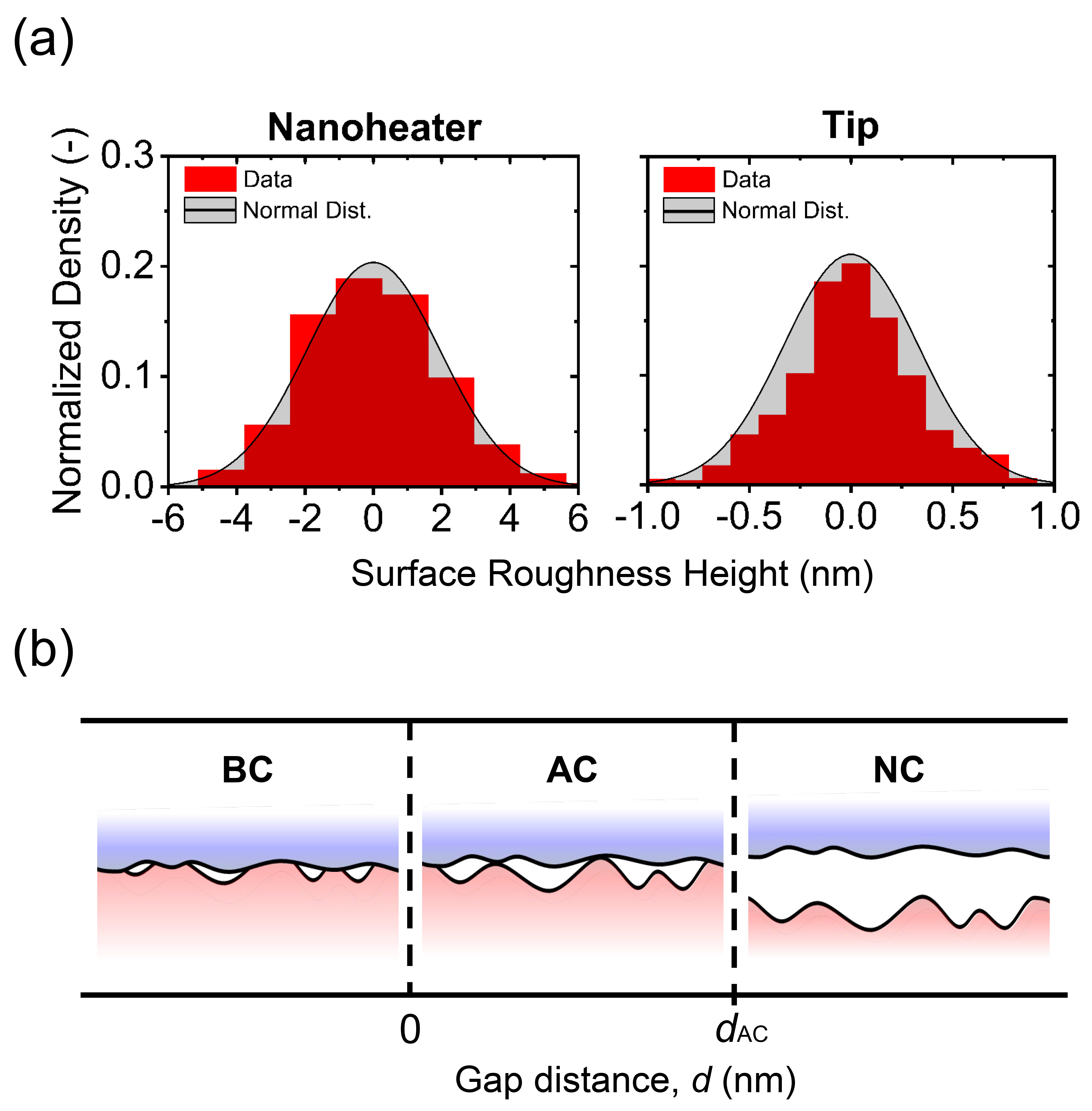
To consistently describe the thermal and force interactions around contact, we define the tip-nanoheater gap () as the distance between the mean lines of the tip and nanoheater surface profiles. \textcolorredTo avoid any undesired inaccuracy due to surface contamination, both the tip and nanoheater surfaces undergo cleaning procedures outlined in Appendix A. The surface profiles of both the Pt nanoheater sensing region and flattened Si tip are then measured by atomic force microscopy as described in Appendix B. As shown in Fig. 2(a), the measured surface profiles for both surfaces follow Gaussian distributions, from which the surface roughness is determined to be nm for the nanoheater sensing area and nm for the Si tip within a 98% confidence interval. As illustrated in Fig. 2(b), the bulk-contact (BC) regime is thus defined as , where the majority of surface asperities are in solid contact. The near-contact (NC) regime is where is larger than the surface peak heights (i.e., , where ) to ensure no contact between surface asperities. The asperity-contact (AC) regime resides between the BC and NC regimes.
The benefit of combining the feedback-controlled nanoheater and HV-SFM platform is the simultaneous measurement of tip-induced thermal transport and conservative tip-nanoheater lateral force interaction. Figure 3 shows the and traces, respectively, as the Si tip is approached to the sensing region of the feedback-controlled nanoheater. The approaching speed of the sample stage is 0.75 nm/s to provide sufficient time to stabilize at the set point of 467.13 K within 50 mK accuracy. While monotonically increases as the nanoheater approaches the tip, its z-derivative shown in the inset clearly shows a drastic drop when the tip makes bulk contact with the nanoheter surface. The onset of bulk contact can also be confirmed by the trace, which drops at the mechanically determined BC point. \textcolorredThe nanoheater feedback controller, which is optimized to provide the best signal-to-noise ratio in and measurements, is not fast enough to fully respond to the abrupt increase of conduction heat transfer through the bulk-contacted Si-Pt interfaces. The slow feedback control is also responsible for the slight drift of by 0.1 K from the set point when the tip is in the AC regime near the BC point. Nevertheless, this result suggests that the onset of BC can be concurrently determined from mechanical and thermal signals and be used as a reference point for the tip-nanoheater gap distance (i.e., ).
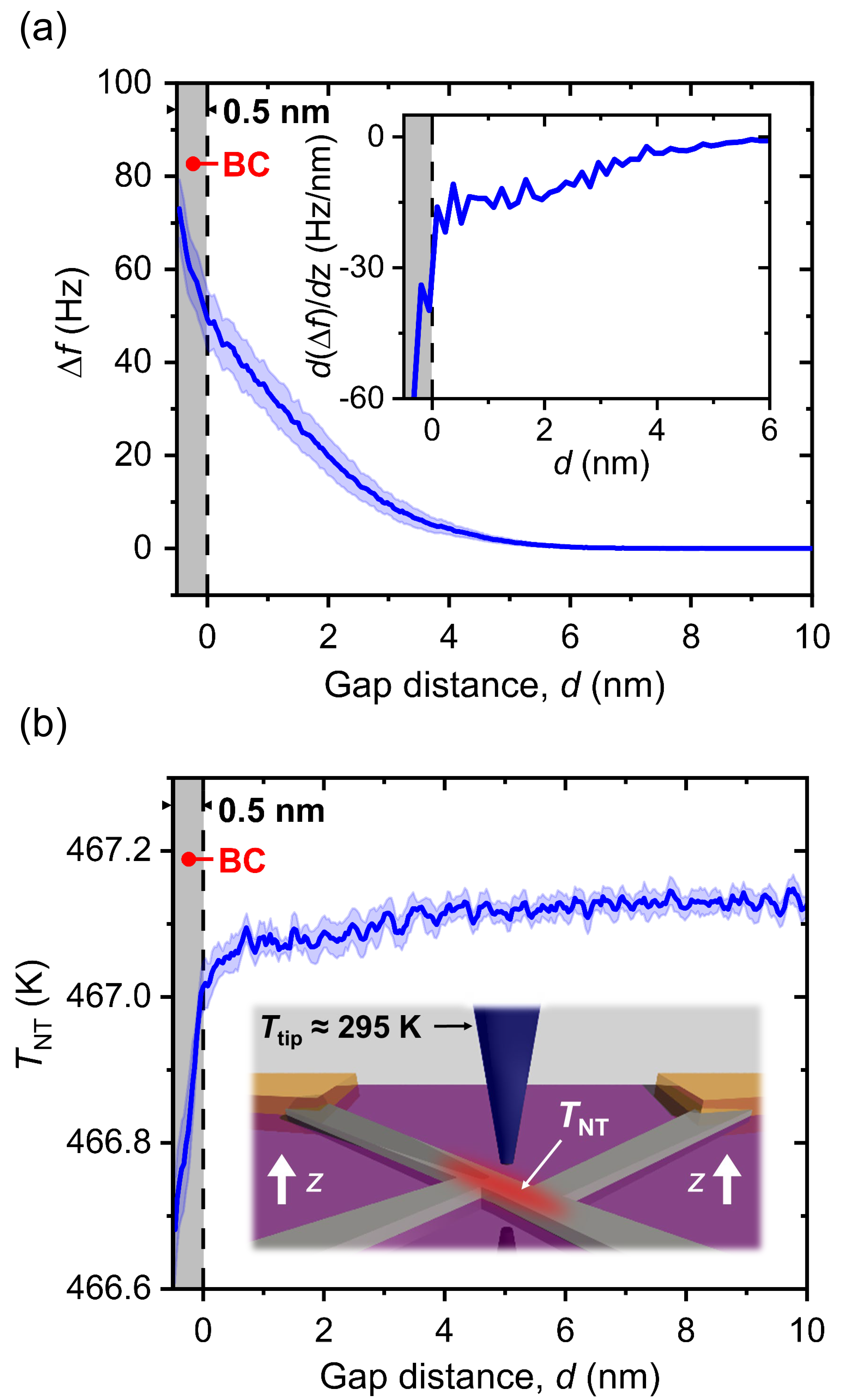
redThe heat transfer rate from the nanoheater sensing region to the tip () can be measured by monitoring that changes to maintain at a set-point while the tip approaches the nanoheater sensing region. However, it should be noted that is the averaged temperature of the nanoheater sensing region. Although is maintained constant under feedback control, tip-induced local cooling perturbs a temperature distribution of the nanoheater to cause heat conduction from the Joule-heated electrical leads to the sensing region (). The tip-based heat transfer rate is thus determined by . Based on the effective thermal network analysis, can be modelled as , where is the Lorentz number, is the length of the sensing region, is the effective length of the lead from the inner electrode to the lead hotspot, and is the difference of power dissipation in the lead with () and without () tip-induced cooling. The derivation of and details of notation are provided in Section I.D of the Supplemental Material [SI_Jarzembski]. When is set to 467.13 K, is estimated to be 4.2% of the measured . The experimental thermal conductance is then defined as , where is the temperature difference between the nanoheater sensing region and the tip apex. Since is not directly measurable, it is assumed to be the same as the tip base temperature at . Section I.E of the Supplemental Material supports this assumption by numerically calculating the thermal conductance of the tip, which is two orders of magnitude greater than the BC thermal conductance [SI_Jarzembski].
2.3 Measurement of
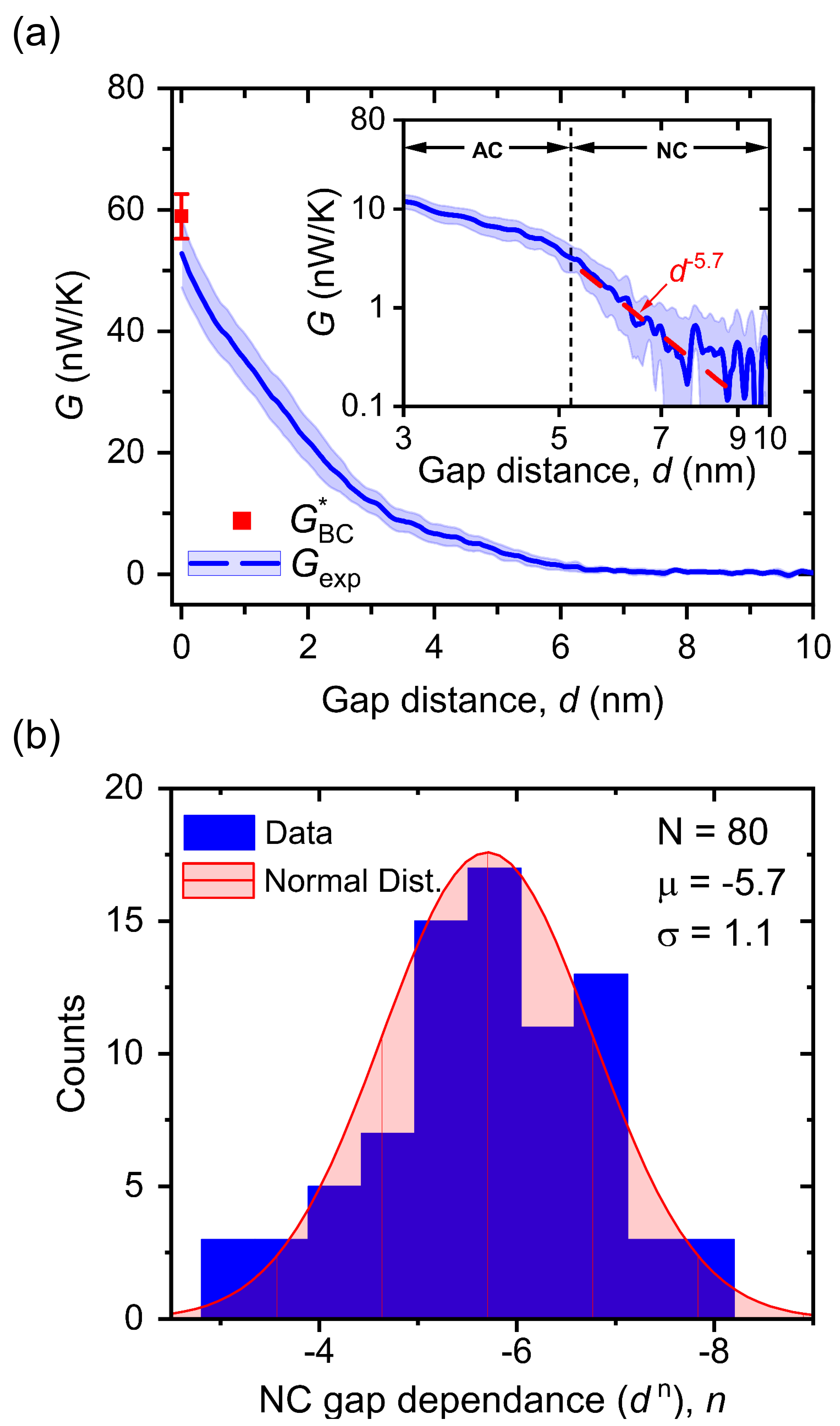
In Fig. 4(a), the experimental thermal conductance shows a monotonically increasing trend as the gap distance decreases, approaching the adjusted BC thermal conductance () of 58.9 3.7 nW/K. It should be noted that was separately measured using a cantilever probe and adjusted by considering the difference in tip apex geometry: see Appendix C for more details. When is re-plotted on a log-log scale as shown in the inset of Fig. 4(a), the curve displays different gap dependencies between the NC regime and the AC regime. In the NC regime, increases by an order of magnitude from the nanoheater noise threshold (i.e., 0.4 nW/K) following a power law. In order to confirm the reproducibility of the observed NC gap dependence (), we repeated the measurement 80 times using three different tip-nanoheater sets and extracted values. Each data fits well with the function in the NC regime as quantified by an average R2-value of 0.87. Figure 4(b) shows the histogram of values, which is well represented by a Gaussian distribution to yield . On the other hand, the AC regime exhibits a smaller gap dependence than due to the increasing contribution of conduction heat transfer through asperity contacts. In the AC regime, increases by another order of magnitude approaching at .
3 Theoretical Modeling
The experimental thermal conductance conveys a combination of non-contact and contact heat transfer mechanisms that are complicated to model. The gap dependence of in the NC regime (i.e., ) is much steeper than what has been predicted with the existing NFRHT models for the tip-plane configuration [Rousseau2009a, Kim2015a, Edalatpour2016, Jarzembski2017], suggesting that NFRHT may not be the dominant heat transfer mechanism in the NC regime. To elucidate the physics underlying the measured thermal conductance, \textcolorredthe theoretical thermal conductance, , is calculated by considering acoustic phonon transport and NFRHT between tip and nanoheater surfaces that are regenerated based on the measured surface roughness distribution. Since commercial Si microcantilevers are typically n-doped, we consider that the Si tip is n-doped with phosphorus at cm-3 based on the electrical resistance range provided by the manufacturer. The heat transfer coefficient due to electron tunneling has also been calculated using the framework described in Ref. [Tokunaga2021], and its contribution has been found to be orders of magnitude smaller than the other heat transfer mechanisms. Throughout the following discussion, the subscripts and refer to the left and right regions that are respectively made of Pt and Si. The temperatures of the left and right regions are fixed at = 470 K and = 300 K.
red
3.1 Heat transfer coefficient contributions
Heat transfer due to acoustic phonon transport is calculated via the AGF method [Sadasivam2014] applied to a one-dimensional (1D) Si-Pt atomic chain that has an interatomic vacuum gap distance : See the inset of Fig. 5(a) for the schematic of the 1D atomic chain. \textcolorredThe heat flux due to acoustic phonon transport across the interatomic vacuum distance for the 1D atomic chain is given by [Sadasivam2014]
| (1) |
Here, is the Bose-Einstein distribution function, where is the reduced Planck constant and is the Boltzmann constant. The effective heat transfer area, , is the projected atomic area calculated using an average atomic radius, i.e., , where and are the atomic radius of Pt and Si, respectively [Clementi1967]. The phonon transmission function, , is derived from the AGF method by modeling Pt and Si as semi-infinite leads separated by a device region. The device region contains atoms of Pt and Si separated by the vacuum gap. \textcolorredThe phonon transmission function is written as
| (2) |
where the superscript denotes conjugate transpose. The escape rate of phonons from the device region to the semi-infinite leads, , is defined as
| (3) |
where is the self-energy matrix that can be written as . Here, is the coupling matrix connecting the left () or right () semi-infinite lead with the device region. The coupling matrix is computed via the force constant between the atoms bounding the semi-infinite leads and the device region, and the atomic masses. The atomic masses of Pt and Si are and , respectively [Meija2016]. The term is the uncoupled Green’s function (also called surface Green’s function) derived from the harmonic matrix of the left () or right () semi-infinite lead. The uncoupled Green’s function is computed using the decimation technique described in Ref. [Sadasivam2014]. In Eq. (2), the device Green’s function () is given by
| (4) |
where is the identity matrix, and is the harmonic matrix of the device region.
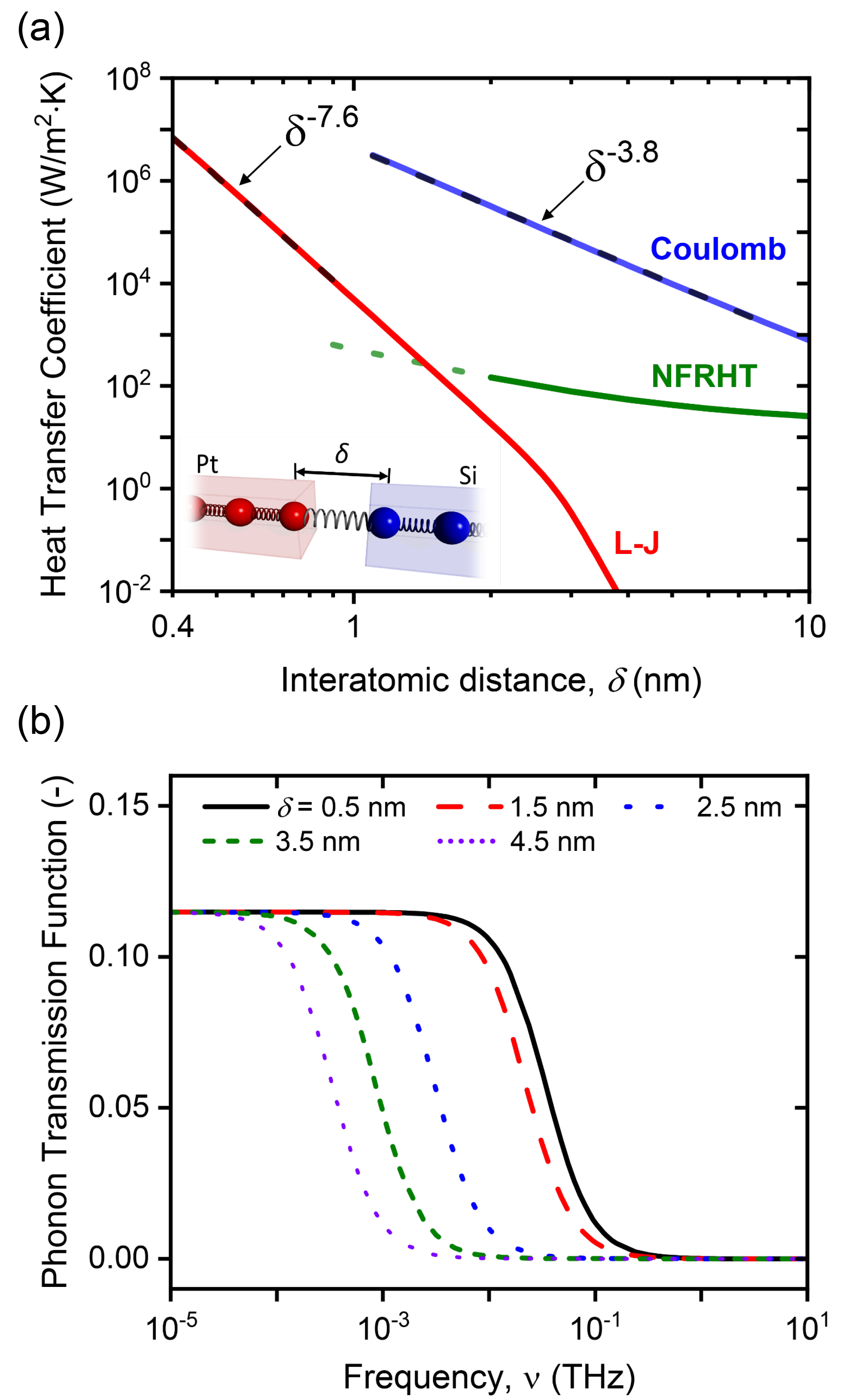
redHeat transfer due to acoustic phonon transport is mediated by short-range and long-range forces in the vacuum region. The overlapping electron cloud repulsive force and van der Waals (vdW) force interactions, modeled by the Lennard-Jones (L–J) potential with empirical parameters for Pt and Si [Webb1996], and the Coulomb force due to surface charges on the nanoheater sensing region, are considered as interatomic forces that virtually connect the Pt and Si atomic chains. \textcolorredDetails regarding calculation of force constants acting in the vacuum space are provided in Appendix D. \textcolorredThe force constants are then included in the harmonic matrix following the procedure described in Appendix E. \textcolorredThe heat transfer coefficient is finally obtained by dividing the heat flux by the temperature difference, i.e., . Five atoms of Pt and five atoms of Si in the device region are sufficient to obtain stable and converged results. Note that \textcolorredalthough the 1D AGF calculation does not capture the angle dependence of phonon propagation and force interactions with neighboring atoms, a previous work [Chiloyan2015b] demonstrated that phonon transport becomes quasi 1D in the NC regime. This has also been verified by comparing 1D AGF results against three-dimensional lattice dynamics results [Alkurdi2020]: More discussion on the verification of the 1D AGF method for calculating interfacial and near-contact acoustic phonon transport is provided in Section II of the Supplemental Material [SI_Jarzembski].
redThe heat transfer coefficient due to NFRHT is calculated using fluctuational electrodynamics [Rytov1989], where Pt and Si are modeled as two semi-infinite planes [Polder1971, Tokunaga2021]. The dielectric functions are taken from Ref. [Djurisic1997] for Pt and Refs. [Fu2006, Basu2010a] for n-doped Si. The radiative heat transfer coefficient is calculated down to an interatomic vacuum distance of 1 nm. However, since fluctuational electrodynamics is a theory based on the macroscopic Maxwell equations that is unlikely to be valid for such a small distance, the NFRHT results below nm are plotted with a dotted curve.
redFigure 5(a) shows the individual contribution of the L–J and Coulomb forces to the AGF-calculated acoustic phonon heat transfer coefficient for the 1D Si-Pt atomic chain. While the L–J force model drives heat transfer for 1.1 nm, the Coulomb force becomes a dominant contributor for larger values (i.e., 1.1 nm 10 nm). This significant contribution of the Coulomb force arises from surface charges induced by the local voltage bias at the center of the nanoheater sensing region (0.8 V from the ground) when it is Joule-heated at 467.13 K. Here, we assume that the Coulomb force vanishes for 1.1 nm due to surface charge neutralization between the nanoheater and tip: See also Appendix D. As a result, acoustic phonon heat transfer between Pt and Si surfaces can exceed NFRHT for interatomic distances up to 10 nm. The potential inaccuracy of the NFRHT calculations has no impact on the theoretical thermal conductance since heat transfer is largely dominated by acoustic phonon transport for 2 nm. The calculated heat transfer coefficients follow power laws of for the L-J force and for the Coloumb force, respectively, illustrating that the experimental value of could be indicative of acoustic phonon transport. Figure 5(b) shows the phonon transmission function calculated by the AGF method, where the dominant frequency range of phonon transmission is below 1.0 THz at 0.5 nm. The phonon dispersion curves and density of states for bulk Pt and Si [Sun2008, Esfarjani2011] confirm that acoustic phonons are the dominant heat carriers across the vacuum distance in the NC regime.
red
3.2 Comparison between and
red For fair comparison with , the theoretical thermal conductance () is calculated by implementing surface features of the flattened Si tip and the Pt nanoheater sensing region in the AGF calculation. To this end, both surfaces are randomly regenerated from the measured surface roughness distributions shown in Fig. 2(a) and discretized into flat pixels having different gap distances. Once the local heat transfer coefficient is calculated by applying the 1D AGF for each pixel, the thermal conductance is approximated as , where is the pixel area and is the local interatomic distance for each pixel. The minimum value of (i.e., contact) is set to 4.68 Å, which is the average value of the lattice constants for Pt (3.92 Å) [Feibelman2001] and Si (5.43 Å) [Esfarjani2011]. The effective heat transfer area, limited by the Si tip surface, is determined based on the SEM image shown in Fig. 1(c). We approximate the Si tip surface as a square whose diagonal length is 240 nm, yielding . is discretized into sub-surfaces of equal size (i.e., . A convergence analysis revealed that is sufficient to obtain stable results. In order to develop statistically relevant predictions, is calculated from 30 regenerated surfaces, which results in 30 sets of .
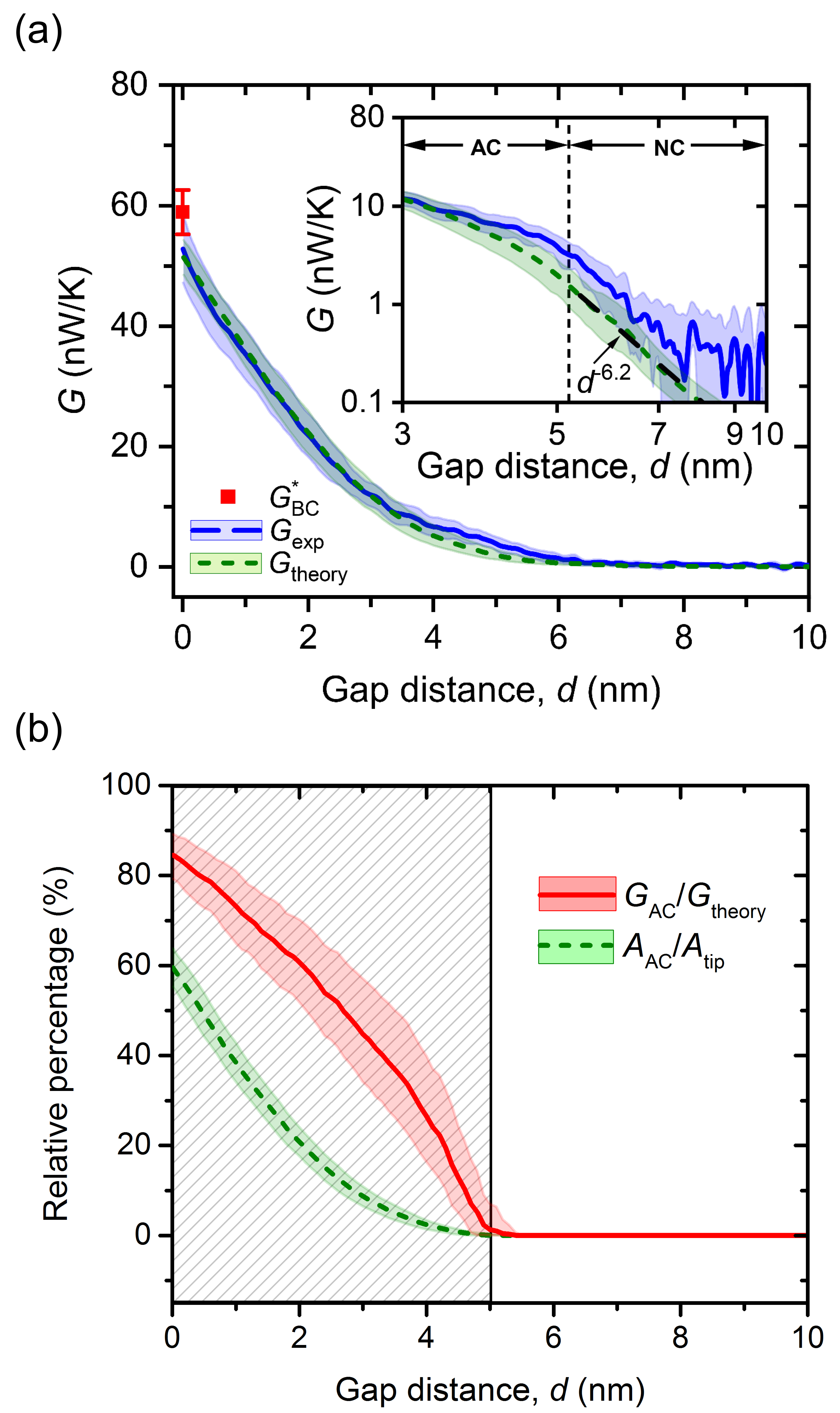
Figure 6(a) compares and on linear-linear and log-log scales (inset), demonstrating strong agreement between them for both NC and AC regimes. \textcolorredThe bold dashed lines (green color) correspond to the theoretical thermal conductance averaged over 30 regenerated surfaces, while the shaded regions (green color) are produced by calculating , where is the standard deviation for the upper and lower bounds of the surface charge density: See Appendix D. The gap dependence of in the NC regime is , which is consistent with the measured gap dependence of within the uncertainty. In addition, the theoretical thermal conductance at (54.2 nW/K) is in good agreement with the bulk thermal conductance values measured with the QTF probe (52.8 nW/K) and the cantilever probe (58.9 nW/K). These well-agreed experimental and theoretical results strongly suggest that acoustic phonon transport play a significant role in heat transfer between Si and Pt for both the NC and AC regimes, possibly being the mechanism bridging radiation and conduction heat transfer. Moreover, the AGF method can separate the contributions of phonon transport through the vacuum gap () and asperity contacts () towards the total thermal conductance (i.e., ). Figure 6(b) shows the asperity-contact thermal conductance ratio () and the asperity-contact area ratio (, where is the asperity-contact area and is the total tip area). While both and are % in the NC regime signifying non-contact heat transfer, they start to increase at nm due to the onset of asperity contacts. It should be noted that the vertical dashed line drawn in the inset of Fig. 6(a) denotes , which is in agreement with the aforementioned definition of the NC and AC regimes (i.e., ) based on the surface roughness. At , reaches 80% of while becomes 60% of , theoretically supporting the smooth transition from near-contact to bulk-contact heat transfer by means of acoustic phonon transport.
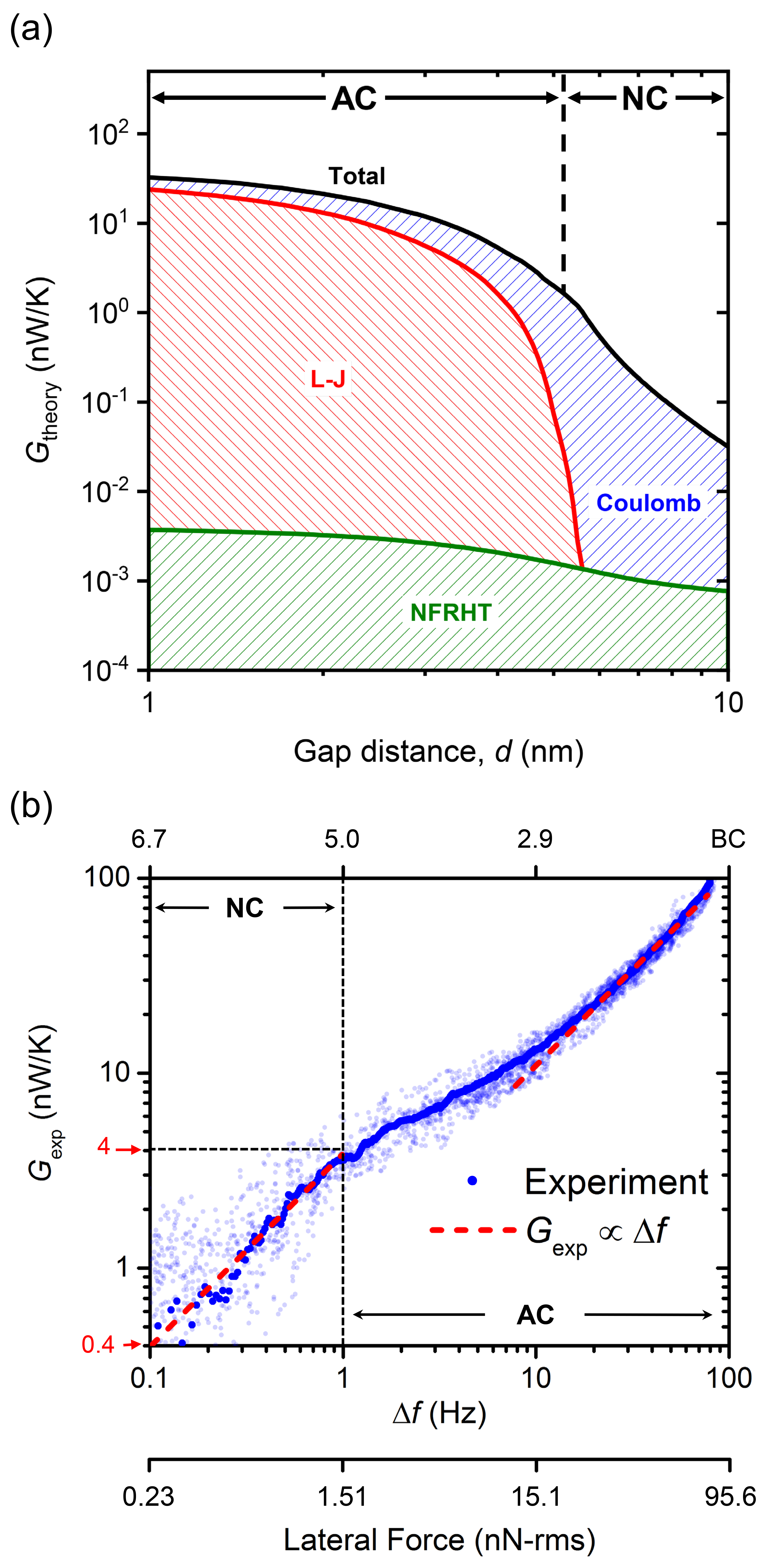
Since acoustic phonon transport across a vacuum gap is mediated by interatomic force interactions between Pt and Si atoms, the impact of each force contributing to is calculated with the AGF method and shown in Fig. 7(a). Here, NFRHT is also included for comparison. In the AC regime, the short-range force interactions, such as the repulsive force due to overlapping electron clouds and the vdW force, dominate thermal transport. However, the Coulomb force becomes a dominant contributor in the NC regime, allowing acoustic phonon transport to exceed NFRHT by up to three orders of magnitude. When considering the origin of the Coulomb force, our calculation suggests the possibility of manipulating heat transfer in the NC regime with external force stimuli [Pendry2016]. Figure 7(b) further demonstrates the strong correlation between tip-surface heat transfer and force interactions by comparing to the simultaneously acquired of the QTF. As the contact regime transitions from AC to BC, becomes linearly proportional to as indicated by the red dashed line in the top right corner of Fig. 7(b). \textcolorredSince the lateral force gradient exerted on the tip can be first-order approximated as [Castellanos-Gomez2011], the lateral force at different gaps can be calculated by integrating the equation over the interval . The calculated lateral force is denoted in Fig. 7(b) along with . Since the lateral force can be related with the normal force by the nanoscale friction law [Mo2009], the observed linear proportionality in the AC-to-BC transition indicates a strong correlation between the normal contact force and the interfacial thermal conductance. Interestingly, a similar linear proportionality between and is observed in the NC regime as indicated by the red dashed line in the bottom left corner, implying that Pt and Si atoms are still connected by interatomic forces to allow non-contact acoustic phonon transport. We also experimentally demonstrate that the tip-sample lateral force increases with the increasing electrical current supplied to the nanoheater in the NC regime (Section III of the Supplemental Material [SI_Jarzembski]), which we believe should increase the thermal conductance. However, the manipulation of the near-contact thermal conductance by external force stimuli was not measured due to limitations in the current nanoheater design, which remains a future research.
4 Conclusions
We have conducted experiments of thermal transport between a flattened Si tip and feedback-controlled Pt nanoheater in a high-vacuum shear force microscope (HV-SFM) as the tip is positioned in the near-contact (NC), asperity-contact (AC), and bulk-contact (BC) regimes with the nanoheater surface. The obtained experimental results clearly show that heat transfer in the NC regime is much greater than NFRHT with a stronger gap dependence. Comparison of the experimental data with heat transfer calculations based on the atomistic Green’s function method and fluctuational electrodynamics frameworks provides evidence that acoustic phonons can be transported not only through asperity contacts but also across nanoscale vacuum spaces due to force interactions between terminating atoms separated by vacuum. This finding sheds light on the possibility of engineering interfacial thermal transport using external force stimuli, which can impact the development of next-generation thermal management technologies.
Acknowledgements
This work was supported by the National Science Foundation (CBET-1605584) and the Nano Material Technology Development Program (2015M3A7B7045518) through the National Research Foundation of Korea (NRF). A.J. acknowledges financial supports from the University of Utah’s Sid Green Fellowship and the National Science Foundation Graduate Research Fellowship (No. 2016213209). T.T. acknowledges support from the Yamada Science Foundation and the Fujikura Foundation. C.S. acknowledges support from the National Science Foundation Graduate Research Fellowship (No. 2017249785). The support and resources from the Center for High Performance Computing at the University of Utah are gratefully acknowledged. 3D schematics were generated using the open-source software POV-ray (www.povray.org). We also thank Prof. Takuma Shiga at the University of Tokyo for fruitful discussions.
red
Appendix
red
4.1 Surface cleaning procedures
redTo ensure that the interacting surfaces are free from contamination prior to experiments, a routine surface inspection and cleaning protocol was established for the QTF probes and nanoheaters. First, several QTF probes and nanoheaters are inspected using scanning electron microscopy (SEM) to select the ones with no major debris around the sensing areas: see Figs. 1(c) and (d). After initial sonication cleaning with acetone, they are placed in a deep ultraviolet (UV) ozone cleaner (Novascan, PSD-UV4) to remove organic contamination using UV light at 185 and 254 nm in wavelength [Tsao2007]. The UV-ozone cleaner is set to generate ozone for 2 hours. After UV treatment, the QTF probe and the nanoheater are promptly mounted to the HV-SFM, which is evacuated to high vacuum to minimize undesired exposure to the ambient before experiments [Cui2017a]. Moreover, all experiments were carried out at high temperature (i.e., 467 K), which inherently removes weakly bonded contaminants from the surface.
red
4.2 Surface roughness characterization
redIn order to secure a sufficient heat transfer area, the Si tip was flattened by long-line scanning on the nanoheater substrate (i.e., a 500-nm thick silicon nitride film on top of a silicon substrate) at a contact force of 10 nN. Once the flattened tip was attached to the QTF, the tip was long-line scanned on the nanoheater substrate again in asperity contact mode for the fine adjustment of surface parallelism. Since the surface profiles play a pivotal role in determining different contact regimes, we measured the surface roughness distributions of both the nanoheater sensing region and flattened Si tip. The nanoheater surface profile was obtained by soft-contact AFM imaging, as marked by a yellow rectangle in Fig. 1(d). A small contact force ( 3 nN) during the AFM imaging results in a contact diameter of 8 nm as estimated by the Hertzian model [Derjaguin1975]. A surface roughness histogram of the nanoheater sensing region from the obtained AFM image shows a Gaussian distribution centered at 0 nm with a standard deviation of 1.96 nm: see Fig. 2(a). The equivalent surface peak height is nm within a 98% confidence interval. The surface profile of a flattened Si tip was determined by tapping-mode topographic imaging of a calibration sample consisting of sharp pyramids (K-TEK Nanotechnology, TGT1), whose apex radii are nominally 17 nm. Since the sample pyramids are much sharper than the flattened Si tip, the resulting convoluted tip-sample AFM image provides the surface roughness profile of the flattened tip. A surface roughness histogram of the flattened tip area from the convoluted AFM image displays a Gaussian distribution centered at 0 nm with a standard deviation of 0.33 nm, as shown in Fig. 2(a). The equivalent surface peak height is nm within a 98% confidence interval.
red
4.3 Measurement of bulk-contact thermal conductance
redTo fully understand the transition from NC to BC thermal transport, the tip should approach the nanoheater sensing region to form BC while avoiding damage to the tip and nanoheater. However, the high vertical rigidity of the QTF can easily damage both the tip and nanoheater when the tip is further pushed once BC is made. To address this challenge, we conducted BC measurements separately by using a cantilever in high vacuum (see Fig. S7(a) in the Supplemental Material [SI_Jarzembski]). It should be noted that our HV-SFM also has a regular AFM head for cantilever-based operations. The cantilever used in the BC experiment is the same model (Bruker, FMV-A) as mounted to the QTFs for the NC and AC measurements. The cantilever deflection is detected by an optical fiber interferometer aligned with the cantilever’s backside [Rugar1989]. Nanoheater #2 was used for the BC measurement (topography shown in Fig. S7(b)), whose sensing area is 330 nm 375 nm. After AFM topographic imaging with soft-contact mode ( 3 nN), the force spectroscopy measurement was conducted by approaching the tip to the nanoheater sensing region until they make hard contact ( 15 nN). An SEM image of the Si tip after the force spectroscopy is shown in Fig. S7(c). We believe that bulk contact is made at the flattest portion of the tip apex to form the contact diameter of 21525 nm.
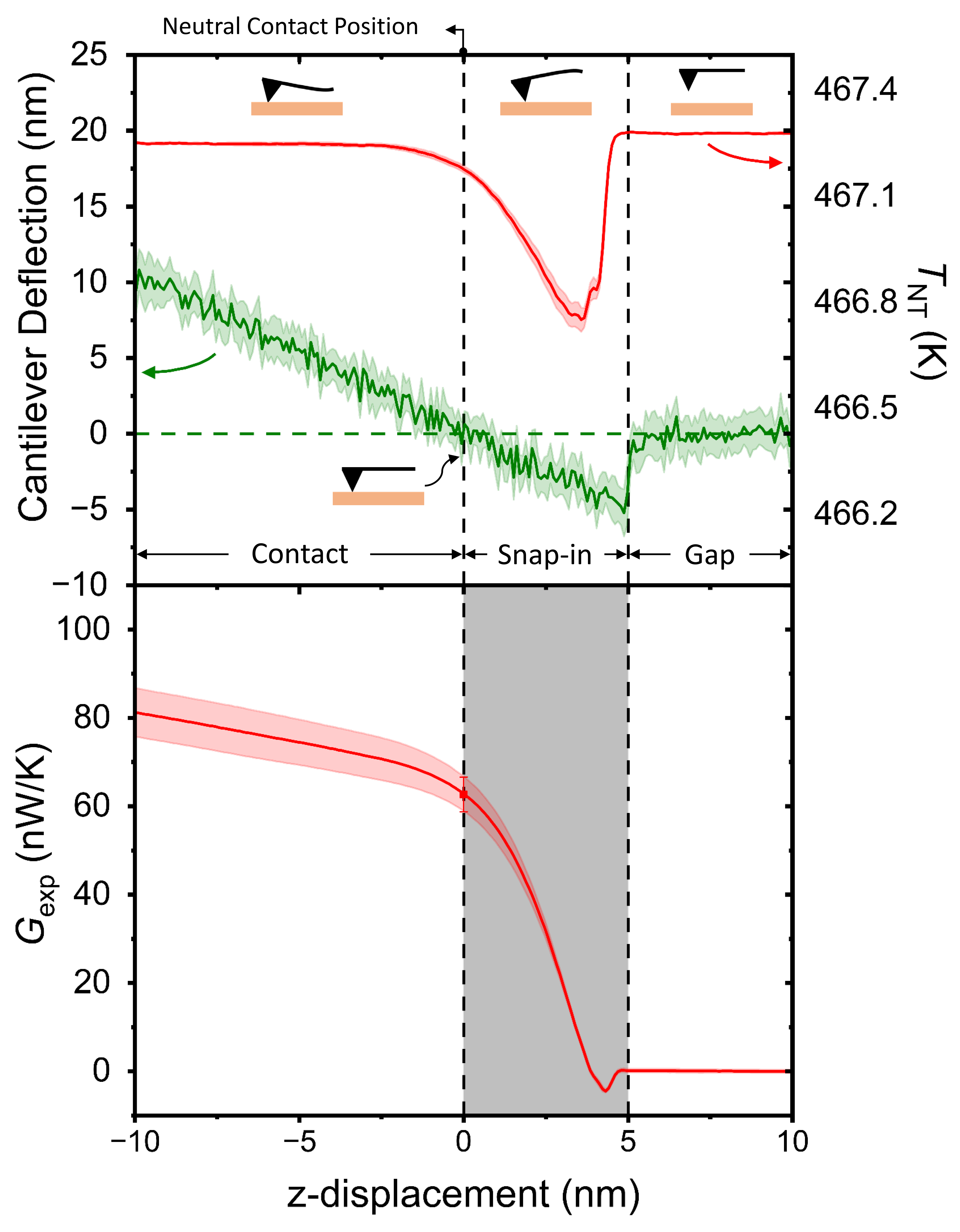
redFor both the cantilever- and QTF-based experiments, the nanoheater current () is feedback-controlled while the voltage drop across the sensing region () is measured for real-time monitoring of . The only difference in the cantilever-based measurements is that after snap-in-contact is made, the cantilever is further pushed to achieve BC between the tip and nanoheater. Figure 8 presents the cantilever deflection and signals as a function of the tip position. At a distance of 5 nm, the cantilever snaps into contact as denoted by the sudden drop of the cantilever deflection and . As the tip is continuously pushed toward the nanoheater, the cantilever returns to its neutral position, which is referred to as the zero z-displacement position [Kim2015a]. In the negative displacement regime, the sample pushes the cantilever to bend backwards such that bulk contact is made with a sufficient contact force. Meanwhile, the feedback controller settles to the set-point by increasing the heating power. Figure 8 also shows the corresponding value of , which remains zero in the gap region, rapidly increases at snap-in, and gradually increases as the cantilever is further pushed. The gradual increase of the thermal conductance is indicative of the onset of bulk contact and is attributed to the pressure dependence of the interfacial thermal resistance [Gotsmann2013]. From this measurement, the BC thermal conductance () between the Si tip and Pt nanoheater is determined to be 62.7 3.9 nW/K at nm. For proper comparison with the QTF-based experiments, the obtained is adjusted by considering the different effective contact area. The adjusted thermal conductance, , is estimated to be 58.9 3.7 nW/K and is shown in Figs. 4(a) and 6(a).
red
4.4 Calculation of force constants for the AGF method
redThe short-range electron cloud interaction and van der Waals force are modeled via the L–J potential, while the long-range electrostatic surface charge interaction is modeled with the Coloumb force [Shockley1948]. The L–J force constant is given by: \textcolorred
| (5) |
redwhere and for the interaction between Pt and Si atoms (Pt-Si)[Webb1996]. \textcolorredThe interatomic force constant of Pt, , is obtained from Eq. (5) using and for Pt-Pt interaction [Webb1996], whereas is taken from Ref. [Ezzahri2014] for Si-Si interaction. Although the tip used in the experiments is made of n-doped Si (phosphorus-doped at ), it is treated as intrinsic Si in the AGF calculations because the elastic constant of n-doped Si is nearly the same as that of intrinsic Si for doping levels up to .[Ono2000]
redThe Coulomb force is mediated by surface charges. The Pt nanoheater sensing region has negative surface charges due to the applied bias voltage of 0.8 V as measured from the ground. By conceptualizing the Si tip as a floating ground, positive image charges are induced at the tip apex. Surface charges of opposite signs are the source of the Coulomb force. The Coulomb force constant due to surface charges is given by [Terris1989]:
| (6) |
where is the permittivity of free space, and is the surface charge (= , where is the surface charge density). \textcolorredPrediction of is challenging as it depends on the material properties, bias voltage, temperature, and gap distance. To constrain these parameters for our experimental condition, we extract from the the gap-dependent signal of the QTF at = 6 nm, where is independently measured from the nanoheater signals and contains the effects of those parameters onto the tip-sample force. It should be noted that the Coulomb force is expected to be dominant at = 6 nm, which is in the NC regime.
redAt = 6 nm, the lateral force is calculated to be 0.42 nN-rms. In addition, we assume = 0.0005 as the near-contact friction coefficient that correlates the lateral force with the normal force. This value is within the acceptable range for the Si-Pt system with a nanoscale gap because experimental measurements of the contact value ranges from 0.1 to 0.01 depending on the contacting area [Bhushan2007]. Furthermore, molecular dynamics simulations for lubricated atomically flat surfaces in contact predicted [Gao2004]. Using , is estimated to be using the Coulomb force equation [Tokunaga2021]. We establish a confidence interval for the near-contact ranging from 0.001 to 0.0004, which corresponds to a surface charge density range of to . These surface charge density values are in the reasonable range when compared with previous works [Yang2007b, Johann2009, ElKhoury2016, Klausen2016] and used to determine the theoretical uncertainties in conjunction with the surface roughness distributions as shown in Figs. 6(a) and (b). \textcolorredIt should be noted that at a small vacuum distance before contact, the Coulomb force vanishes due to charge neutralization [Behrens2001]. The present work treats as a constant value that vanishes at a specific cutoff gap distance [Butt1991] due to the difficulty of describing its gap-dependence. The cutoff distance is determined at the onset of electron tunneling across the vacuum gap, which is defined at an interatomic distance [Anselmetti1994, McCarty2008].
red
4.5 Incorporation of force constants into the harmonix matrix
redThe force constants of the vacuum region due to the Lennard-Jones potential () and Coulomb interactions () are incorporated into the harmonic matrix in Eq. (4) as follows [Sadasivam2014]:
\textcolorred{gather}
\boldsymbolH_d = {bmatrix}
⋱& ⋮ ⋮ ⋮ ⋮ \iddots
⋯ H^4,4_d -k_Pt/m_Pt 0 0 ⋯
⋯ -k_Pt/m_Pt H^5,5_d -(k_L-J + k_Coulomb)/m_Si 0 ⋯
⋯ 0 -(k_L-J + k_Coulomb)/m_Pt H^6,6_d -k_Si/m_Si ⋯
⋯ 0 0 -k_Si/m_Si H^7,7_d ⋯
\iddots ⋮ ⋮ ⋮ ⋮ ⋱
\textcolorredThe components of the harmonic matrix are described as . The force constants of the Pt and Si atoms are given by and , and their atomic weight are denoted as and , respectively. The device region includes a total of 10 atoms (5 Si atoms for the left side and 5 Pt atoms for the right side), thus resulting in a 10 10 harmonic matrix. The diagonal components of are calculated by
\textcolorred
| (7) |