Direct Measurement of Quantum Efficiency of Single Photon Emitters in Hexagonal Boron Nitride
Abstract
Single photon emitters in two-dimensional materials are promising candidates for future generation of quantum photonic technologies. In this work, we experimentally determine the quantum efficiency (QE) of single photon emitters (SPE) in few-layer hexagonal boron nitride (hBN). We employ a metal hemisphere that is attached to the tip of an atomic force microscope to directly measure the lifetime variation of the SPEs as the tip approaches the hBN. This technique enables non-destructive, yet direct and absolute measurement of the QE of SPEs. We find that the emitters exhibit very high QEs approaching at wavelengths of , which is amongst the highest QEs recorded for a solid state single photon emitter.
I Introduction
Two-dimensional (2D) materials exhibit unique optoelectronic, nanophotonic and quantum effects, that are not possible with their bulk counterparts Novoselov et al. (2016); Mak and Shan (2016); Urbaszek and Srivastava (2019); Toth and Aharonovich (2019). Hexagonal Boron Nitride (hBN) is one such material, that has attracted considerable attention due to its ability to host ultra bright single photon emitters (SPEs) that operate at room temperature Tran et al. (2016); Kianinia et al. (2017); Proscia et al. (2018); Kim et al. (2018); Jungwirth et al. (2016); Grosso et al. (2017). The emitters are point defects (impurity, missing atoms or vacancy complexes), embedded in the lattice of hBN. Recent efforts have focused on understanding the photophysical properties of these defects, with the goal to increase their brightness, stability, and yield Tawfik et al. (2017); Wigger et al. (2019); Feldman et al. (2019); Ngoc My Duong et al. (2018); Vogl et al. (2018); Xu et al. (2018).
An important parameter that up to now has been unknown for the family of SPEs in hBN is their quantum efficiency (QE). The QE is an important parameter of any light source to be considered for implementation in practical devices. However, measuring the quantum efficiency of solid state sources is challenging due to the significantly varying surrounding electromagnetic environment.
In this work, we utilise a recently engineered family of SPEs in a few nm thick hBN films, grown by chemical vapor deposition (CVD). These exhibit less wavelength variability than commercial hBN sources and also provide a flat topography over large area Mendelson et al. (2019); Comtet et al. (2019); Lin et al. (2017), which is advantageous for our experiments. To measure the QE, we utilise a method that was pioneered by Drexhage in the 1970s, Drexhage (1970) who investigated changes in the intrinsic radiative decay rate of europium ions as a function of distance to a silver mirror. The underlying modification of spontaneous emission of the emitters in close proximity to a metal surface is a quantum electrodynamic effect and related to local density of states (LDOS)Barnes (1998); Novotny and Hecht (2006); Schell et al. (2014); Beams et al. (2013); Anger et al. (2006). Since the intrinsic non-radiative decay rate is not modified by the LDOS, changes in the total decay rate can be attributed to an alteration of the radiative decay rate alone. In this way, radiative and non-radiative decay rate components can be separated by recording the emitter’s excited state lifetime as a function of its distance to a mirror. Hence, this fundamental technique to directly measure the QE from decay rate components has been used for organic dyes, rare earth ions, quantum dots, and color centers in diamond. Buchler et al. (2005); Lunnemann et al. (2013); Karaveli et al. (2013); Kwadrin and Koenderink (2012)
II Experimental setup
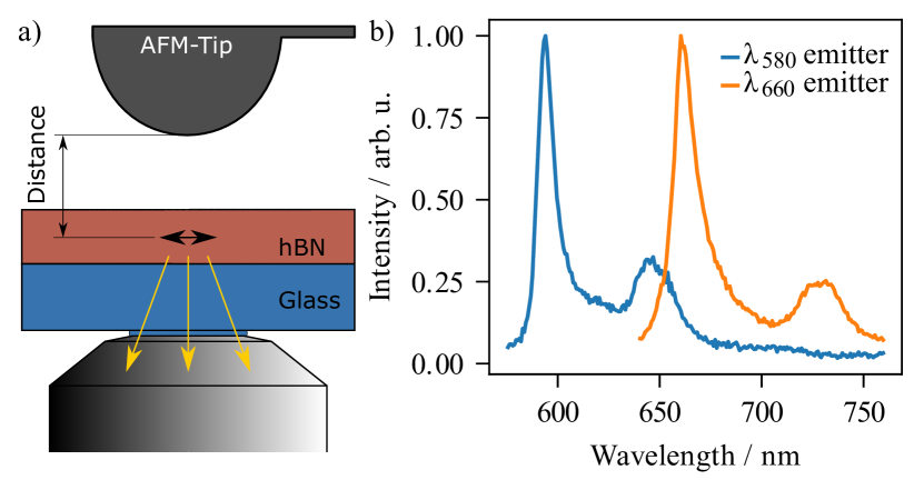
The schematics of the measurement setup is shown in Fig. 1 a). A wavelength tunable pulsed laser (Solea, Picoquant) is focused through the cover slide onto the hBN flake with an oil immersion objective lens (NA 1.4, 100x). The SPE fluorescence is collected via the same objective lens and guided through a confocal setup into a Hanbury-Brown and Twiss setup, consisting of a polarizing beam splitter (PBS) and two avalanche photon diodes (APD) (Excelitas). With a -plate before the PBS we analyzed the fluorescence polarization, finding it to be parallel to the glass substrate, an example of which is shown in the suplemental material ????. The SPEs in hBN were grown using a CVD method as described elsewhere Mendelson et al. (2019). The hBN flakes were then transferred onto transparent glass substrate, to enable simultaneous atomic force microscope (AFM) and photo luminescence (PL) measurements. Two examples of single emitters in the hBN flakes are shown in Fig. 1 b. To measure the QE of the SPEs, modification of their LDOS was achieved by employing a hemispherical tip with a radius of covered by gold. Modifications of the emitter’s lifetime were obtained by changing the distance of the AFM tip to the emitter. The lateral position of the tip and focus of the excitation laser were matched by scanning the tip over a large area while recording laser light reflected by the tip. Once matched, the mirrors’ vertical position could be changed precisely via the build-in AFM piezo, allowing distance-dependent measurements of the SPE properties.
The QE can be considered as a scaling factor between a change in LDOS and a change in emission rate, as non-radiative processes are unaffected by a changed LDOS. A detailed discussion can be found in Ref. Drexhage (1970). The equation used to relate QE and LDOS is given by:
| (1) |
With the distance-dependent lifetimes , LDOS and QE , analogue to Ref. van Dam et al. (2018); Amos and Barnes (1997). Accordingly, a change in LDOS is mediated by changing the mirror distance, which finally reveals the QE.
III Simulation of expected lifetime changes
In order to relate the change in distance of emitter and mirror to a change in LDOS, we performed a simulation of an emitter exhibiting a horizontally polarized dipole hosted in the center of a thick hBN layer (refractive index of ) situated on top of a glass substrate. A hemisphere made from gold with a tip radius is centered at a distance from the dipole acting as a mirror that changes the local density of states (LDOS) . The LDOS can be expressed Novotny and Hecht (2006) by
| (2) |
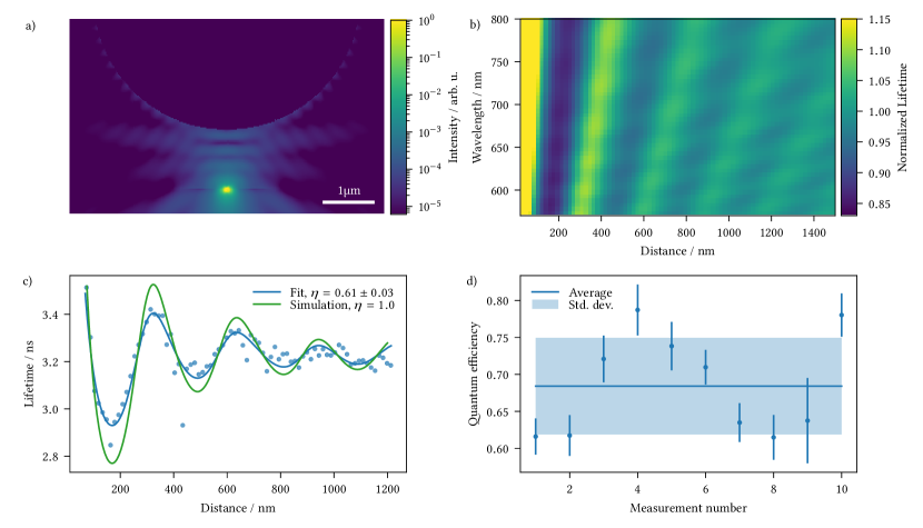
with the distance dependent emitted power , which can be extracted from the simulation. Only SPEs with in-plane polarization were found (e.g. shown in the supplemental material ????), therefore the simulations were performed with an in-plane polarized dipole. An intensity distribution with and an emission wavelength of is shown in Fig. 2 a). In this situation, a standing wave pattern between dipole and mirror with three nodes can be seen. Similar simulations at different wavelength and distances were performed and relative lifetime changes extracted, results are shown in Fig. 2 b).
IV Quantum efficiency measurement
Once an SPE was identified, we performed distant-dependent lifetime measurements for various tip to the emitter distances. First, we fixed the AFM tip to emitter distance at approximately . At this point, we performed a lifetime measurement for . Next we reduced the distance by and performed the next lifetime measurement, repeating this process until reaching the surface. The built-in AFM laser points at the end of the cantilever and gets reflected to a build-in four quadrant photo diode. A bending of the cantilever results in a change in position of the laser on the photo diode, which was used to indicate a completed approach to the surface and thus stopped the QE measurement. Since this method has an error margin of at least one step () and we don’t know the emitter’s depth, we keep a distance offset as a fit parameter. The emission wavelength is also kept as a fit parameter within reasonable limits deducted from the measured spectrum. The maximum distance for lifetime measurements was which was sufficient to produce robust values for the lifetime at infinity when left as a fit parameter.
To determine the QE, we fitted the following function to the distance-dependent lifetime measurements:
| (3) |
Fig. 2 c) shows one representative QE measurement (dots) of a SPE with a QE of , with a corresponding fit of Eq. 3 (blue solid line). For comparison, a case for an emitter with (green solid line) is also plotted.
To determine the error margins of the QE values, we performed 10 measurements on the same emitter shown by dots in Fig. 2 d). From this data set we calculated the average and the standard deviation of , represented by the solid line and the shaded area, respectively. In the following discussion and figures, we used this standard deviation. In a reference measurement, changed within minutes by about one standard deviation, uncorrelated to AFM tip approaches (see supplementary material ????). Thus we speculate that photoinduced changes of the environment may cause lifetime and QE variations.
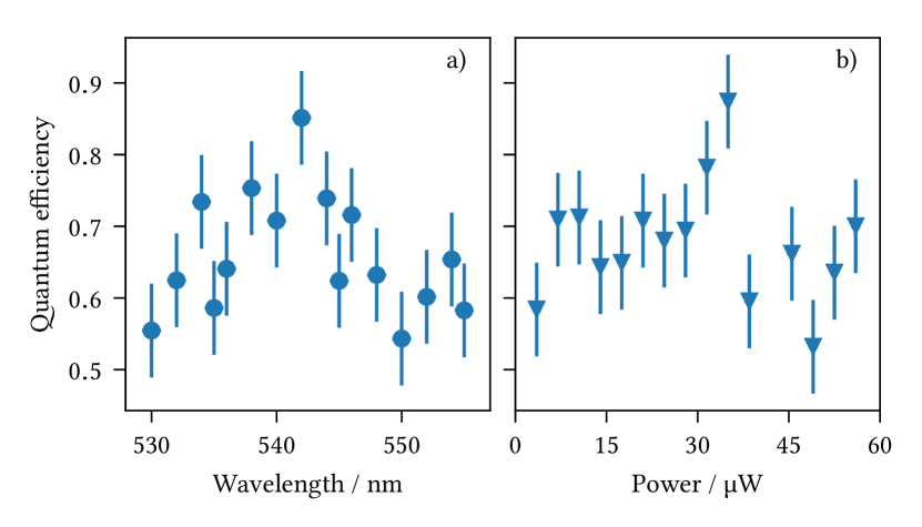
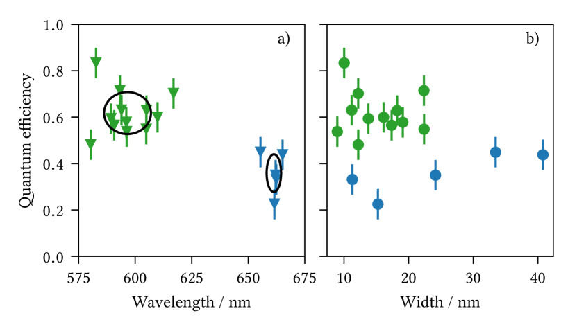
Fig. 3 a) shows the QE dependence on the excitation wavelength, conducted at an emitter with a ZPL wavelength of emitter. In addition, a power dependent QE measurement was performed on the same emitter, using an excitation wavelength of . However, no systematic trend can be seen, as shown in Fig. 3 b). We therefore conclude that the QE of the hBN emitters are independent of the excitation wavelength or power, which indicates an isolated electronic structure without shelving or additional non radiative states. Most SPEs in the CVD grown hBN sample show ZPL central positions at Mendelson et al. (2019) when excited with wavelength of . We denote this family as . Consequently, we selected 12 emitters from this family at random and performed QE measurements on each of them. Interestingly, however, when we switched the excitation laser to , a second family of emitters shows up with ZPL central positions at , which we term emitters Comtet et al. (2019). These emitters were less common throughout the samples, and we were only able to identify five SPEs with clear ZPL (see Fig. 1 b for example of the SPE). The family may be associated with a different charge state or an altered absorption cross-section pathway. Exciting the same area of hBN with a laser wavelength in between and , didn’t show any emitters with ZPL positions in between the original ZPL wavelengths. Consequently, we compared the QE of these two families, with the results plotted in Fig. 4 a). We find clear evidence that the emitters with the higher energy ZPL possess a higher QE. The QE of the obtained from averaging over 12 SPEs, while the QE of the family with the longer ZPLs is , averaged over 5 emitters, respectively. We also compared the full width at half maximum (FWHM) of the emitters in both families, as shown in Fig. 4 b). According to our results, there was no clear trend between the FWHM and the QE, for both families. This might be counter-intuitive, since it indicates that the coupling to low energy phonons does not result in non radiative transitions. Nevertheless, the clear difference in the QE values indicate that the two families have isolated electronic structures (rather than being same emitter that is shifted by strain or electric fields).
V Summary
To summarize, we presented a method to measure the absolute QE of SPEs in hBN. Accompanied by a simulation of the change in LDOS, we found record high QEs of single SPEs in hBN approaching . By measuring the QE of 17 SPEs and relating them to the respective ZPL wavelength, we could identify two SPE families, well separated in ZPL position, with different QEs. One family showing ZPLs clustered around showed an average QE of , while the other family operating at showed an average QE of . While the crystallographic origin of the defects is yet unknown, our results suggest that these emitters possess two distinct electronic structures. Having ultra thin (few nm) solid state SPEs with high QEs opens up fascinating opportunities for advanced quantum photonic experiments. For instance, combining these emitters with dielectric antennas that have near unity collection efficiency, may result in a room temperature ”single photon gun” Chu et al. (2017). Such sources can also find use in quantum cryptography, that has traditionally been utilizing faint laser sources due to lack of ultra bright and ultra-pure SPEs. The SPEs in hBN that possess the higher QE can potentially meet this demand. Finally, the presented method can be extended to measure QE of localized and interlayer excitons in other 2D materials Rivera et al. (2015).
VI Funding
Financial support from the German Ministry of Education and Research (BMBF) project ”NANO-FILM”, the Australian Research council (via DP180100077, DP190101058), the Asian Office of Aerospace Research and Development grant FA2386-17-1-4064, the Office of Naval Research Global under grant number N62909-18-1-2025 are gratefully acknowledged. I.A. is grateful for the Humboldt Foundation for their generous support. O.B. acknowledges the UTS Distinguished Visiting Scholars scheme.
VII Acknowledgments
N. N. thanks Bastian Leykauf and Carlo Bradac for fruitful discussions
References
- Novoselov et al. (2016) K. S. Novoselov, A. Mishchenko, A. Carvalho, and A. H. C. Neto, Science 353, aac9439 (2016).
- Mak and Shan (2016) K. F. Mak and J. Shan, Nature Photonics 10, 216 (2016).
- Urbaszek and Srivastava (2019) B. Urbaszek and A. Srivastava, Nature 567, 39 (2019).
- Toth and Aharonovich (2019) M. Toth and I. Aharonovich, Annual Review of Physical Chemistry 70, 042018 (2019).
- Tran et al. (2016) T. T. Tran, K. Bray, M. J. Ford, M. Toth, and I. Aharonovich, Nature Nanotechnology 11, 37 (2016).
- Kianinia et al. (2017) M. Kianinia, B. Regan, S. A. Tawfik, T. T. Tran, M. J. Ford, I. Aharonovich, and M. Toth, ACS Photonics 4, 768 (2017).
- Proscia et al. (2018) N. V. Proscia, Z. Shotan, H. Jayakumar, P. Reddy, C. Cohen, M. Dollar, A. Alkauskas, M. Doherty, C. A. Meriles, and V. M. Menon, Optica 5, 1128 (2018).
- Kim et al. (2018) S. Kim, J. E. Fröch, J. Christian, M. Straw, J. Bishop, D. Totonjian, K. Watanabe, T. Taniguchi, M. Toth, and I. Aharonovich, Nature Communications 9, 2623 (2018).
- Jungwirth et al. (2016) N. R. Jungwirth, B. Calderon, Y. Ji, M. G. Spencer, M. E. Flatté, and G. D. Fuchs, Nano Letters 16, 6052 (2016).
- Grosso et al. (2017) G. Grosso, H. Moon, B. Lienhard, S. Ali, D. K. Efetov, M. M. Furchi, P. Jarillo-Herrero, M. J. Ford, I. Aharonovich, and D. Englund, Nature Communications 8, 705 (2017).
- Tawfik et al. (2017) S. A. Tawfik, S. Ali, M. Fronzi, M. Kianinia, T. T. Tran, C. Stampfl, I. Aharonovich, M. Toth, and M. J. Ford, Nanoscale 9, 13575 (2017).
- Wigger et al. (2019) D. Wigger, R. Schmidt, O. Del Pozo-Zamudio, J. A. Preuß, P. Tonndorf, R. Schneider, P. Steeger, J. Kern, Y. Khodaei, J. Sperling, S. M. de Vasconcellos, R. Bratschitsch, and T. Kuhn, 2D Materials 6, 035006 (2019).
- Feldman et al. (2019) M. A. Feldman, A. Puretzky, L. Lindsay, E. Tucker, D. P. Briggs, P. G. Evans, R. F. Haglund, and B. J. Lawrie, Physical Review B 99, 020101 (2019).
- Ngoc My Duong et al. (2018) H. Ngoc My Duong, M. A. P. Nguyen, M. Kianinia, T. Ohshima, H. Abe, K. Watanabe, T. Taniguchi, J. H. Edgar, I. Aharonovich, and M. Toth, ACS Applied Materials & Interfaces 10, 24886 (2018).
- Vogl et al. (2018) T. Vogl, G. Campbell, B. C. Buchler, Y. Lu, and P. K. Lam, ACS Photonics 5, 2305 (2018).
- Xu et al. (2018) Z.-Q. Xu, C. Elbadawi, T. T. Tran, M. Kianinia, X. Li, D. Liu, T. B. Hoffman, M. Nguyen, S. Kim, J. H. Edgar, X. Wu, L. Song, S. Ali, M. Ford, M. Toth, and I. Aharonovich, Nanoscale 10, 7957 (2018).
- Mendelson et al. (2019) N. Mendelson, Z.-Q. Xu, T. T. Tran, M. Kianinia, J. Scott, C. Bradac, I. Aharonovich, and M. Toth, ACS Nano , acsnano.8b08511 (2019).
- Comtet et al. (2019) J. Comtet, E. Glushkov, V. Navikas, J. Feng, V. Babenko, S. Hofmann, K. Watanabe, T. Taniguchi, and A. Radenovic, Nano Letters , acs.nanolett.9b00178 (2019).
- Lin et al. (2017) W.-H. Lin, V. W. Brar, D. Jariwala, M. C. Sherrott, W.-S. Tseng, C.-I. Wu, N.-C. Yeh, and H. A. Atwater, Chemistry of Materials 29, 4700 (2017).
- Drexhage (1970) K. H. Drexhage, J. Lumin. 1-2, 693 (1970).
- Barnes (1998) W. L. Barnes, J. Mod. Opt. 45, 661 (1998).
- Novotny and Hecht (2006) L. Novotny and B. Hecht, Principles of Nano-Optics (Cambridge University Press, Cambridge, 2006).
- Schell et al. (2014) A. W. Schell, P. Engel, J. F. M. Werra, C. Wolff, K. Busch, and O. Benson, Nano Letters 14, 2623 (2014).
- Beams et al. (2013) R. Beams, D. Smith, T. W. Johnson, S.-H. Oh, L. Novotny, and A. N. Vamivakas, Nano Letters 13, 3807 (2013).
- Anger et al. (2006) P. Anger, P. Bharadwaj, and L. Novotny, Phys. Rev. Lett. 96, 113002 (2006).
- Buchler et al. (2005) B. C. Buchler, T. Kalkbrenner, C. Hettich, and V. Sandoghdar, Phys. Rev. Lett. 95, 63003 (2005).
- Lunnemann et al. (2013) P. Lunnemann, F. T. Rabouw, R. J. A. Van Dijk-Moes, F. Pietra, D. Vanmaekelbergh, and A. F. Koenderink, ACS Nano 7, 5984 (2013).
- Karaveli et al. (2013) S. Karaveli, A. J. Weinstein, and R. Zia, Nano Lett. 13, 2264 (2013).
- Kwadrin and Koenderink (2012) A. Kwadrin and A. F. Koenderink, J. Phys. Chem. C 116, 16666 (2012).
- van Dam et al. (2018) B. van Dam, C. I. Osorio, M. A. Hink, R. Muller, A. F. Koenderink, and K. Dohnalova, ACS Photonics 5, 2129 (2018).
- Amos and Barnes (1997) R. M. Amos and W. L. Barnes, Physical Review B 55, 7249 (1997).
- Chu et al. (2017) X.-L. Chu, S. Götzinger, and V. Sandoghdar, Nature Photonics 11, 58 (2017).
- Rivera et al. (2015) P. Rivera, J. R. Schaibley, A. M. Jones, J. S. Ross, S. Wu, G. Aivazian, P. Klement, K. Seyler, G. Clark, N. J. Ghimire, J. Yan, D. G. Mandrus, W. Yao, and X. Xu, Nature Communications 6, 6242 (2015).