Large tunneling magnetoresistance in VSe2/MoS2 magnetic tunnel junction
Abstract
Two-dimensional (2D) van der Waals (vdW) materials provide the possibility of realizing heterostructures with coveted properties. Here, we report a theoretical investigation of the vdW magnetic tunnel junction (MTJ) based on VSe2/MoS2 heterojunction, where the VSe2 monolayer acts as the ferromagnet with the room-temperature ferromagnetism. We propose the concept of spin-orbit torque (SOT) vdW MTJ with reliable reading and efficient writing operations. The non-equilibrium study reveals a large tunneling magnetoresistance (TMR) of 846 % at 300 Kelvin, identifying significantly its parallel and anti-parallel states. Thanks to the strong spin Hall conductivity of MoS2, SOT is promising for the magnetization switching of VSe2 free layer. Quantum-well states come into being and resonances appear in MTJ, suggesting that the voltage control can adjust transport properties effectively. The SOT vdW MTJ based on VSe2/MoS2 provides desirable performance and experimental feasibility, offering new opportunities for 2D spintronics.
Centre de Nanosciences et de Nanotechnologies, CNRS, Université Paris-Sud, Université Paris-Saclay, Palaiseau 91120, France
![[Uncaptioned image]](/html/1904.07499/assets/x1.png)
Keywords: vdW heterojunction, magnetic tunnel junction, tunnel magnetoresistance, spin Hall effect, ab initio calculation
1 Introduction
Two-dimensional (2D) van der Waals (vdW) materials, with the strong covalent intralayer bonding and the weak vdW interlayer interaction, exhibit novel properties and various advantages1, 2, 3, 4. Recently, the investigations on ferromagnetic vdW materials make great progress5, 6, 7, 8 and experimental advances have demonstrated that ferromagnetic order can persist in the ultrathin atomic limit9, 10. Monolayer CrI3 has been reported to be an Ising ferromagnet with perpendicular magnetic anisotropy (PMA) and 45 Kelvin Curie temperature. 11 After that, Fe3GeTe2 was demonstrated to possess robust 2D ferromagnetism in monolayer with PMA and 130 Kelvin Curie temperature,12 and the ionic gate raises the Curie temperature of Fe3GeTe2 to 300 Kelvin13. Moreover, the intrinsic room-temperature ferromagnetism was found in VSe2 monolayers14, 15. 1T phase VSe2 monolayers were grown by molecular beam epitaxy (MBE) on MoS2 and graphene substrates, respectively, and MoS2 has been proved to be a good substrate for the uniform growth of ferromagnetic VSe2 monolayer.
Ferromagnetic materials are pivotal in the spintronics device, e.g., magnetic tunnel junction (MTJ), which employs the relative magnetization orientation to store binary data.16 MTJ presents high conductance for two ferromagnetic layers in the parallel configuration (PC), while low conductance for two ferromagnetic layers in the anti-parallel configuration (APC), and the difference between the two kinds of conductance is the tunneling magnetoresistance (TMR) effect. MTJs based on vdW materials have been studied a lot.17, 18, 19. Thanks to the perfect spin filtering effect, high magnetoresistances were predicted in the graphene/Ni (Co) systems through ab initio calculations. 20 The spin valve device using MoS2 as the nonmagnetic spacer was prepared, and its magnetoresistance effect was investigated experimentally and theoretically.21 Magnetic vdW materials were also employed as the ferromagnetic layer in several works. The tunneling spin valve has been prepared with two exfoliated Fe3GeTe2 crystals and h-BN tunnel layer, and the TMR signal reached up to 160 % at 4.2 Kelvin.22 More intriguingly, the switching of Fe3GeTe2 has been achieved via spin-orbit torque (SOT) induced by spin Hall effect (SHE). 23, 24 The vdW heterojunctions consisting of CrI3 exhibit more superior TMR performances. Layer-dependent magnetic phases have been observed in CrI3-based MTJ,25 and TMR was drastically enhanced with increasing CrI3 layer thickness, reaching up to 19000 % at the ultra-low temperature of 2 Kelvin. Works above reveal the possibility to shrink the MTJ scale to the atomically scale with versatile vdW materials, as well as the TMR enhancement and SOT switching in vdW MTJs. However, to the best of our knowledge, the room-temperature TMR remains absent in experimental works of vdW MTJs. Besides, the conventional magnetic field switching hinders the scaling down of vdW MTJ.
In this work, we design the SOT vdW MTJ based on VSe2/MoS2 heterojunction. By the ab initio calculation, we investigated the intrinsic spin Hall conductivity (SHC) of MoS2, which is the MTJ bottom layer for writing current injection. The SHC of MoS2 is tunable and considerable, which suggests that SOT is a promising switching method. We studied the spin-resolved transport properties of the SOT vdW MTJ, revealed the quantum-well resonances in vdW layers, and discovered a non-equilibrium TMR up to 846 % at 300 Kelvin. With the merit of experimental feasibility, the SOT vdW MTJ provides efficient writing and reliable reading operations at the room temperature, as well as practical prospects for spintronics device.
2 Methods
The calculations of structure optimization were performed using the density functional theory (DFT) approach implemented in the VASP code,26 considering the optB88-vdW function and the Hubbard U term. The calculation of SHC was performed by Quantum ESPRESSO and WANNIER90 packages.27, 28, 29 The electrical transport properties were calculated using OpenMX package through the DFT combined with non-equilibrium Green function (NEGF) formalism considering the Hubbard term.30 The generalized gradient approximation (GGA) of Perdew-Burke-Ernzerhof (PBE)31 was used to describe the exchange-correlation functional of the electrons. More details can be found in the Supporting Information. At equilibrium state, the spin-resolved conductance is obtained by the Landauer-Büttiker formula
| (1) |
where is the transmission coefficient with spin at the transverse Bloch wave vector and Fermi energy , is the electron charge and is the Planck constant. At non-equilibrium state, the current is calculated as the integral
| (2) |
where is the Fermi distribution function, and are the chemical potentials of the left and right leads, respectively.
3 Results and discussions
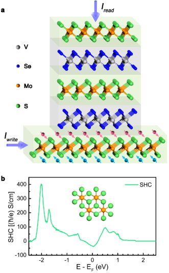
The atomic schematic diagram of the SOT vdW MTJ is shown in Figure 1a. The VSe2 in 1T phase is employed as the ferromagnetic layer. As the magnetization of VSe2 decays with the increasing layer number,32 we only studied the monolayer VSe2 in this work. 1H phase MoS2 is used as the tunnel barrier layer with the band gap of 1.9 eV.33 MoS2 is a good substrate for uniform growth of VSe2,14 thus the VSe2/MoS2 heterojunction has high feasibility in experiments. Apart from the basic MTJ structure, the metallic vdW material, 1T phase MoS2 is adopted as the electrode in the top and bottom of MTJ. Thanks to the advances of synthesis technology,34, 35 metallic 1T phase MoS2 nanosheets can be stabilized and employed as the electrode. 36 The SOT vdW MTJ is symmetrical to keep the most stable interfacial configurations, which have been confirmed by VASP calculations. Details about the optimized structure can be found in Figure S1 in Supporting Information.
The basic manipulations of MTJ include reading and writing operations. Several mechanisms can be employed in the writing process, such as the external magnetic field,22 the spin transfer torque (STT),37 as well as SOT. 23 The magnetic field switching impedes the device miniaturization, while the STT is not feasible due to the low spin polarization of 1T VSe2. 38 With the merits of simple device structure, high reliability, and remarkable efficiency, we choose SOT switching in the vdW MTJ. One of SOT mechanisms is spin Hall effect (SHE), which is a phenomenon that spin-orbit coupling effect generates an asymmetric deviation of the charge carriers due to the different spin direction39. SHE realizes the conversion from charge current to spin current. In the bilayer system, the ferromagnetic layer would absorb the angular momentum of the spin current in nonmagnetic layer, and achieve SOT switching of magnetization in ferromagnetic layer. 40, 41, 42 SOT switching of Fe3GeTe2 magnetization has been observed in the Fe3GeTe2/Pt bilayer23, 24. SHE in Pt produces a pure spin current, which enters the Fe3GeTe2 layer and induces both field-like and damping-like torques.24 Compared to the conventional SOT devices, high SOT efficiency has been found in the Fe3GeTe2/Pt bilayer. The efficiency enhancement could be attributed to the atomically flat surface, which may conduce to the proximity effect in vdW heterostructures.43 Discussions above illustrate that vdW MTJs have the potential to achieve SOT switching via SHE. As Figure 1a shows, when the writing current is injected into the bottom MoS2 electrode, the spin current arises in the vertical direction with the in-plane spin torque, which can be used to switch the magnetization of the VSe2 layer adjoining to the bottom MoS2 layer. To explore the strength of SHE, we studied the intrinsic spin Hall conductivity (SHC) of 1T MoS2. Results are shown in Figure 1b. Although the SHC at EF is limited to 34 (/e)S/cm, SHC at E = 2.0 eV reaches up to 400 (/e)S/cm. It indicates that gate voltage control is an efficient manipulation to improve SHC. As the SHC in 1T MoS2 is comparable to that in Weyl semimetals with strong SOC44, the MTJ based on VSe2/MoS2 heterojunction is promising to be switched by the SOT effect.
Apart from the writing operation, another critical manipulation in MTJ is the reading process, which relies on the TMR effect. High TMR is a desirable performance for the reliability of MTJ device, and TMR at room temperature is essential to the practical prospect. We studied the TMR in the above-mentioned MTJ, abbreviated as MT MTJ due to the 1H MoS2 tunnel barrier layer. For MT MTJ, we define the PC (APC) as the bottom VSe2 monolayer having the parallel (anti-parallel) magnetic orientation relative to the top VSe2 monolayer, as the bottom VSe2 monolayer is the free layer. Besides, we design a new vdW MTJs with 1H VSe2 as the tunnel barrier layer, abbreviated as VT MTJ. For VT MTJ, we define the PC (APC) as the 1H VSe2 tunnel layer holding the parallel (anti-parallel) magnetic orientation to two 1T VSe2 monolayers, namely, 1H VSe2 is the free layer. 1H VSe2 is the magnetic semiconductor,45 so it is predictable that both tunnel transport and spin filtering would happen in the VT MTJ, as well as high TMR. The interlayer exchange coupling (IEC) in VT MTJ was investigated. It turns out that IEC in VT MTJ is comparable with Fe/MgO/Fe system, indicating the data storage stabilization of VT MTJ. The possibility of VT MTJ switching by anomalous Hall effect was also considered. Details about IEC analysis and VT MTJ switching can be found in Supporting Information.
| MTJs | TMR(%) | ||||
|---|---|---|---|---|---|
| MT MTJ | 225 | 45 | 111 | 111 | 22 |
| VT MTJ | 69 | 182 | 34 | 9 | 484 |
We calculated the spin-resolved conductance and TMR of both MT and VT MTJs at the equilibrium state at 300 Kelvin, and present the results in Table 1. The TMR is defined as at equilibrium state, where and is the total conductance for the PC and APC of MTJ, respectively. , where and is the majority-spin and minority-spin conductance in PC, respectively. , where and is the majority-spin and minority-spin conductance in APC, respectively. The TMR in MT MTJ is only 22 %, however, the VT MTJ presents a much remarkable TMR up to 484 %. In both MTJs, the conductances have the comparable scale in PC while those in APC vary a lot. The in MT MTJ is three times as large as that in VT MTJ, and more distinctly, the in MT MTJ is over one magnitude larger than that in VT MTJ. As the TMR is inversely proportional to , the low results in high TMR in VT MTJ. We attribute the high TMR to the efficient spin filtering effect in APC of VT MTJ, where VSe2 trilayer is stacked in anti-ferromagnetic ordering, blocking spin transport especially for the minority spin in APC. In contrast, the high conductance in APC of MT MTJ damages TMR.
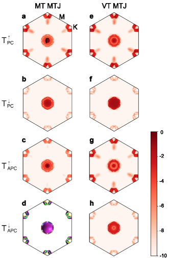
Although the VT MTJ can realize high TMR at equilibrium state, it is not feasible for the SOT vdW MTJ, as the free layer of VT MTJ is in the middle of the device, not adjoin the bottom layer. We may make the bottom 1T VSe2 ferromagnetic layer as the free layer, but the double spin filtering effect would vanish, further impair TMR. Consequently, it is imperative to analyze the factor leading to low TMR and improve it in MT MTJ. According to the Landauer-Büttiker formula, the conductance is the integration of transmission over all points in the 2D Brillouin zone (BZ). We plot the -resolved transmission spectra to present more details in the BZ. Figure 2a-h show the transmission spectra in different spin channels in both MT and VT MTJs except for Figure 2d, which is the Fermi surface of 1T MoS2 electrode, determining the outlines of the transmission spectra. In of MT MTJ, a sharp peak with the at point results in the high conductance in . Due to the symmetrical structure of MT MTJ, the transmission spectra of and is the same at equilibrium state, so we only show the in Figure 2c. A sharp peak arises around point as shown by the deep red color in Figure 2c, inducing in the high conductance in MT MTJ. We find that at point, an extraordinary transmission coefficient for the tunneling transport. On the other hand, for VT MTJ, a remarkable broad peak around point is observed in , and the transmission coefficient is considerable at point, resulting in the high conductance in VT MTJ. Due to the double spin filtering effect in VT MTJ, the transmission in minority-spin channel in Figure 2h is much weaker, as low as at point.
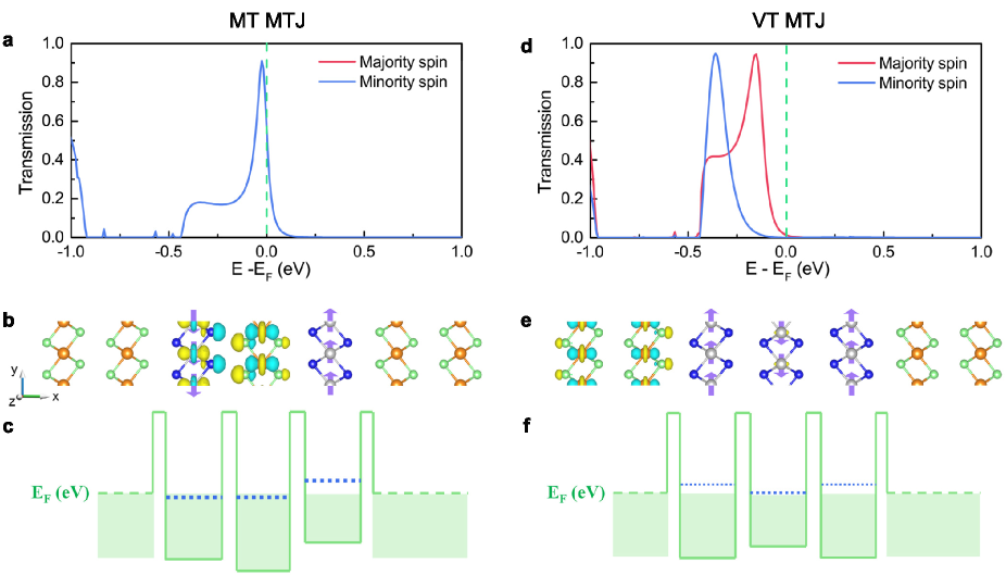
To understand the unusual transmission coefficient and clarify the APC transmission, we present the minority-spin transmission analysis at point for APC of both MT and VT MTJs, where and , respectively. The analysis of components of wavefunctions indicates that the s and px orbitals in S and Se atoms, as well as the s, px, dx2-y2 and dz2 orbitals in Mo and V atoms, make the dominant contribution to the transmission, especially d orbitals. The shapes of px orbitals in S and Se atoms can be observed by the wavefunctions in Figure 3b and d, as well as the dz2 orbitals in Mo and V atoms. Figure 3a shows the transmission versus energy curve in MT MTJ. The transmission peaks of both spins locate approximately at EF, at E = 0.02 eV to be exact. The transmission coefficient at EF is , which is extraordinarily high for tunneling transport. In Figure 3b, it is distinctive that eigenchannel wavefunctions localize at the left VSe2 and the middle MoS2 tunnel layers. Because of the weak interaction among vdW layers and the strong intralayer covalent bond, quantum-well resonances are very likely to arise in vdW heterojunction46, 25. Considering the high transmission and wavefunction localization, we can infer that the quantum-well resonances arise in MT MTJ. Quantum-well states exhibit the localization of the transmission eigenchannel wavefunctions. The electrons are reflected back and forth in the barrier region, forming a standing wave pattern, and results in the almost perfect transmission. Figure 3c gives a more intelligible picture on resonances by the schematic plot of the potential profile. We use blue dot lines in vdW layers to indicate the quantum-well states of the minority spin. The quantum-well states in the left VSe2 and the middle MoS2 tunnel layers are very close to the EF. The match of two quantum-well states results in the resonances of wavefunctions in this area, as well as the intense localization and remarkable transmission. As the quantum well states are sensitive to the location of EF, we studied the transmission with EF shift and present the results in Figure S2. Stronger resonances can be observed at the energy point E = 0.02 eV where transmission , an extremely high coefficient close to 1.
Figure 3d shows the transmission for VT MTJ. Two peaks deviate from the EF. at E = 0.15 eV, and at E = 0.36 eV. Due to the sharp attenuation of transmission, the transmissions at EF for both spins are inconspicuous, resulting in at EF. Figure 3e shows the minority-spin eigenchannel wavefunctions for VT MTJ, the wavefunctions decay along the transport x direction from the incoming MoS2 electrode. Note that for minority spin, both the left 1T VSe2 and the right 1T VSe2 has the prohibitive magnetization, this spin filtering effect results in the fast decay in VT MTJ. We plot the schematic of the potential profile for the model of magnetic quantum wells in VT MTJ, as shown in Figure 3f. Due to the energy mismatch among quantum-well states, no resonance happens and the wavefunctions attenuate very fast along the transport direction. However, the transmission peak at E = 0.15 eV for majority spin and the peak at E = 0.36 eV for minority spin can be explained by the resonance transmission, as shown in Figure S3. Investigations above demonstrate that the vdW heterojunction transport properties are sensitive to the quantum-well resonances, and the Fermi energy shifting can be a practical approach to modulate the transmission of vdW heterojunctions. Note the quantum-well states play a critical role in the high TMR, it is experimentally suggested to keep clean interfaces in the vdW heterojunctions, in order to maintain high TMR and avoid the short-circuiting current. In addition, we present the analysis of transmission at , where high transmission coefficients are observed. The spin-resolved wavefunctions are shown in Fig. S4. Different from the quantum-well states at point, wavefunctions at decay along the transport direction.
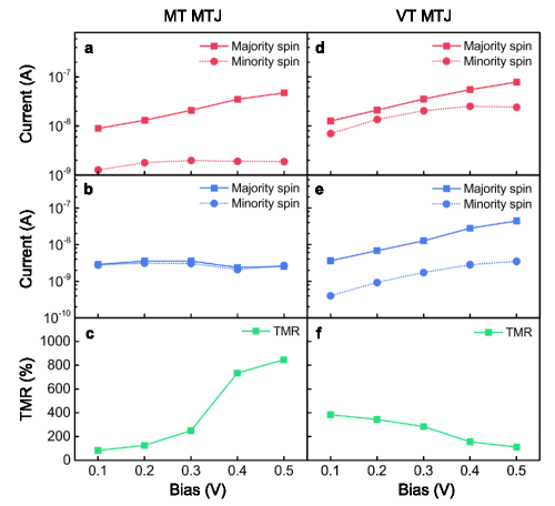
Discussions above illuminate that the quantum-well resonances play an important role in the vdW MTJ at equilibrium state. However, non-equilibrium state tells another story. According to Equation 2, at non-equilibrium state, the current is the integral of transmission with respect to energies in the bias window, rather than the direct result of transmission at EF. In this condition, the quantum-well resonances have limited influence on the non-equilibrium transmission. By observing the APC transmission spectrum of MT MTJ shown in Figure 3a, we found that the states at energies above EF contribute little to the transmission. To reduce the current in APC and get a high TMR, we applied positive bias to the MT MTJ and calculated the non-equilibrium transport properties. As the reference, non-equilibrium transport in VT MTJ was also studied. Figure 4 shows the spin-resolved current and TMR under varying bias. Here the TMR is defined as . We observe that in both MTJs PC currents rise with increasing bias, and majority-spin current is larger than minority-spin current, as shown in Figure 4a and d. More details on current in BZ can be found in Figure S5 and S6. However, APC currents behave distinctly in MT and VT MTJs. Figure 4b shows that in MT MTJ, both majority-spin and minority-spin currents in APC remain almost unchanged with increasing bias, while APC currents in VT MTJ rise with increasing bias, as shown in Figure 4e. Figure S5 and S6 present more details on this difference from the aspect of BZ. In MT MTJ, even if the transmission broadens in the center of BZ, the transmission peak at point weakens a lot with increasing bias. As a result of trade-off, the current in APC almost remains unchanged with bias in APC. In VT MTJ, the current of majority spin around K point strengthens with increasing bias, and the current of minority spin broadens around point, resulting in the APC current enhancement. TMR is inversely proportional to the APC current. Consequently, in MT MTJ, TMR augments with the increasing bias because of the changeless APC current, while TMR in VT MTJ declines due to the enhancement of APC current with increasing bias. TMR of 846 % can be observed at 0.5 V bias in MT MTJ at 300 Kelvin, a considerable result for the room-temperature application. Apart from the calculation at 300 Kelvin, we present the calculation at 100 Kelvin in Fig. S7. It worth stressing that a TMR up to 1277 % is observed in MT MTJ, which is attributed to the decline of APC current at 100 Kelvin. This result provides the potential for TMR improvement by the reduction of temperature.

As the current is obtained by integrating transmission with respect to energies in the bias window, we now turn to the analysis of the transmission versus energy at finite bias. The above analysis illustrates that the APC transmission leads to the difference of TMR in MT and VT MTJs, so we present the result of transmission versus energy for APC, and the transmission is the integration over all points in the BZ, as shown in Figure 5. It can be observed that the transmission spectra for MT MTJ are almost changeless in the bias window for any bias, and the transmission coefficients are approximately zero. The point resonances of quantum-well states at E = 0.02 eV make the electron intensely localized. Under the influence of bias, the resonances shift to the negative energy, at E = 0.08 eV for the 0.5 V bias, out of the bias windows in the non-equilibrium transmission, and result in a suppressed current in APC. On the other hand, in VT MTJ transmission, majority spin contributes more than minority one. With the rising bias, more majority-spin transmission peaks enter into the bias window and contribute to the current. Due to the double spin filtering layer for minority spin, the transmission is suppressed close to zero over all the bias windows. Combining the majority-spin and minority-spin current, the total current in APC increases with bias in VT MTJ. Figure S8 presents the transmission versus energy at 100 Kelvin. It has a similar outline with the transmission spectra at 300 Kelvin. Note that the decreasing temperature declines the conductance in APC of MT MTJ, and results in the TMR enhancement. The analysis above explains the differences between APC currents in MT and VT MTJs, and clarifies the reason for distinct TMR behaviors.
4 Conclusion
In conclusion, we propose an MTJ based on vdW heterojunction consisting of 2D ferromagnet VSe2 and MoS2 monolayer, and validate its performances by ab initio calculation. A large TMR at room temperature over 800 % can be obtained through the voltage control, enhancing the sensitivity of MTJ. Thanks to the considerable and tunable SHC of MoS2, the MTJ is promising to be switched efficiently by SOT. It is important to mention that we fully consider the further practical implementation, as the VSe2 monolayer with room-temperature ferromagnetism has been demonstrated experimentally on the MoS2 substrate. This SOT vdW MTJ offers new prospects for low-dimensional spintronics applications.
The authors thank the National Natural Science Foundation of China (Grant No. 61627813, 61571023), the International Collaboration Project B16001, and the National Key Technology Program of China 2017ZX01032101 for their financial support of this work. This work is supported by the Academic Excellence Foundation of BUAA for PhD Students. The calculations were performed on TianHe-1A supercomputer at National Supercomputer Center in Tianjin.
-
•
Supp_info.pdf: Statement on ab initio calculation methods, VT MTJ properties, optimized structures, eigenchannel wavefunctions, wavefunctions at K’ point, current in BZ, and NEGF transport properties at 100 Kelvin.
References
- Mounet et al. 2018 Mounet, N.; Gibertini, M.; Schwaller, P.; Campi, D.; Merkys, A.; Marrazzo, A.; Sohier, T.; Castelli, I. E.; Cepellotti, A.; Pizzi, G.; Marzari, N. Two-Dimensional Materials From High-Throughput Computational Exfoliation of Experimentally Known Compounds. Nat. Nanotechnol. 2018, 13, 246
- Patel et al. 2019 Patel, A. B.; Machhi, H. K.; Chauhan, P.; Narayan, S.; Dixit, V.; Soni, S. S.; Jha, P. K.; Solanki, G. K.; Patel, K. D.; Pathak, V. M. Electrophoretically Deposited MoSe2/WSe2 Heterojunction from Ultrasonically Exfoliated Nanocrystals for Enhanced Electrochemical Photoresponse. ACS Appl. Mater. Interfaces 2019, 11, 4093–4102
- Zhong et al. 2017 Zhong, D.; Seyler, K. L.; Linpeng, X.; Cheng, R.; Sivadas, N.; Huang, B.; Schmidgall, E.; Taniguchi, T.; Watanabe, K.; McGuire, M. A.; Yao, W.; Xiao, D.; Fu, K.-M. C.; Xu, X. Van der Waals Engineering of Ferromagnetic Semiconductor Heterostructures for Spin and Valleytronics. Sci. Adv. 2017, 3, e1603113
- Tao et al. 2018 Tao, X.; Zhang, L.; Zheng, X.; Hao, H.; Wang, X.; Song, L.; Zeng, Z.; Guo, H. h-BN/graphene van der Waals Vertical Heterostructure: A Fully Spin-Polarized Photocurrent Generator. Nanoscale 2018, 10, 174–183
- Zhao et al. 2016 Zhao, T.; Zhou, J.; Wang, Q.; Kawazoe, Y.; Jena, P. Ferromagnetic and Half-Metallic FeC2 Monolayer Containing C2 Dimers. ACS Appl. Mater. Interfaces 2016, 8, 26207–26212
- Si et al. 2015 Si, C.; Zhou, J.; Sun, Z. Half-Metallic Ferromagnetism and Surface Functionalization-Induced Metal-Insulator Transition in Graphene-Like Two-Dimensional C Crystals. ACS Appl. Mater. Interfaces 2015, 7, 17510–17515
- Duong et al. 2017 Duong, D. L.; Yun, S. J.; Lee, Y. H. Van der Waals Layered Materials: Opportunities and Challenges. ACS Nano 2017, 11, 11803–11830
- Jiang et al. 2018 Jiang, Z.; Wang, P.; Xing, J.; Jiang, X.; Zhao, J. Screening and Design of Novel 2D Ferromagnetic Materials with High Curie Temperature above Room Temperature. ACS Appl. Mater. Interfaces 2018, 10, 39032–39039
- Gong et al. 2017 Gong, C.; Li, L.; Li, Z.; Ji, H.; Stern, A.; Xia, Y.; Cao, T.; Bao, W.; Wang, C.; Wang, Y.; Qiu, Z. Q.; Cava, R. J.; Louie, S. G.; Xia, J.; Zhang, X. Discovery of Intrinsic Ferromagnetism in Two-Dimensional van der Waals Crystals. Nature 2017, 546, 265
- Chen et al. 2018 Chen, Y.; Xing, W.; Wang, X.; Shen, B.; Yuan, W.; Su, T.; Ma, Y.; Yao, Y.; Zhong, J.; Yun, Y.; Xie, X. C.; Jia, S.; Han, W. Role of Oxygen in Ionic Liquid Gating on Two-Dimensional Cr2Ge2Te6: A Non-oxide Material. ACS Appl. Mater. Interfaces 2018, 10, 1383–1388
- Huang et al. 2017 Huang, B.; Clark, G.; Navarro-Moratalla, E.; Klein, D. R.; Cheng, R.; Seyler, K. L.; Zhong, D.; Schmidgall, E.; McGuire, M. A.; Cobden, D. H.; Yao, W.; Xiao, D.; Jarillo-Herrero, P.; Xu, X. Layer-Dependent Ferromagnetism in a van der Waals Crystal Down to the Monolayer Limit. Nature 2017, 546, 270
- Fei et al. 2018 Fei, Z.; Huang, B.; Malinowski, P.; Wang, W.; Song, T.; Sanchez, J.; Yao, W.; Xiao, D.; Zhu, X.; May, A. F.; Wu, W.; Cobden, D. H.; Chu, J.-H.; Xu, X. Two-Dimensional Itinerant Ferromagnetism in Atomically Thin Ge. Nat. Mater. 2018, 17, 778
- Deng et al. 2018 Deng, Y.; Yu, Y.; Song, Y.; Zhang, J.; Wang, N. Z.; Sun, Z.; Yi, Y.; Wu, Y. Z.; Wu, S.; Zhu, J.; Wang, J.; Chen, X. H.; Zhang, Y. Gate-Tunable Room-Temperature Ferromagnetism in Two-Dimensional Ge. Nature 2018, 563, 94
- Bonilla et al. 2018 Bonilla, M.; Kolekar, S.; Ma, Y.; Diaz, H. C.; Kalappattil, V.; Das, R.; Eggers, T.; Gutierrez, H. R.; Phan, M.-H.; Batzill, M. Strong Room-Temperature Ferromagnetism in Monolayers on van der Waals Substrates. Nat. Nanotechnol. 2018, 13, 289
- Lee et al. 2019 Lee, S.; Kim, J.; Park, Y. C.; Chun, S.-H. Atomistic Real-Space Observation of the van der Waals Layered Structure and Tailored Morphology in . Nanoscale 2019, 11, 431–436
- Wolf et al. 2001 Wolf, S. A.; Awschalom, D. D.; Buhrman, R. A.; Daughton, J. M.; von Molnár, S.; Roukes, M. L.; Chtchelkanova, A. Y.; Treger, D. M. Spintronics: a Spin-Based Electronics Vision for the Future. Science 2001, 294, 1488–1495
- Cardoso et al. 2018 Cardoso, C.; Soriano, D.; García-Martínez, N. A.; Fernández-Rossier, J. Van der Waals Spin Valves. Phys. Rev. Lett. 2018, 121, 067701
- Kim et al. 2018 Kim, H. H.; Yang, B.; Patel, T.; Sfigakis, F.; Li, C.; Tian, S.; Lei, H.; Tsen, A. W. One Million Percent Tunnel Magnetoresistance in a Magnetic van der Waals Heterostructure. Nano Lett. 2018, 18, 4885–4890
- Galbiati et al. 2018 Galbiati, M.; Vecchiola, A.; Mañas-Valero, S.; Canet-Ferrer, J.; Galceran, R.; Piquemal-Banci, M.; Godel, F.; Forment-Aliaga, A.; Dlubak, B.; Seneor, P.; Coronado, E. A Local Study of the Transport Mechanisms in MoS2 Layers for Magnetic Tunnel Junctions. ACS Appl. Mater. Interfaces 2018, 10, 30017–30021
- Karpan et al. 2007 Karpan, V. M.; Giovannetti, G.; Khomyakov, P. A.; Talanana, M.; Starikov, A. A.; Zwierzycki, M.; van den Brink, J.; Brocks, G.; Kelly, P. J. Graphite and Graphene as Perfect Spin Filters. Phys. Rev. Lett. 2007, 99, 176602
- Wang et al. 2015 Wang, W.; Narayan, A.; Tang, L.; Dolui, K.; Liu, Y.; Yuan, X.; Jin, Y.; Wu, Y.; Rungger, I.; Sanvito, S.; Xiu, F. Spin-Valve Effect in NiFe//NiFe Junctions. Nano Lett. 2015, 15, 5261–5267
- Wang et al. 2018 Wang, Z.; Sapkota, D.; Taniguchi, T.; Watanabe, K.; Mandrus, D.; Morpurgo, A. F. Tunneling Spin Valves Based on Ge/hBN/Ge van der Waals Heterostructures. Nano Lett. 2018, 18, 4303–4308
- Wang et al. 2019 Wang, X.; Tang, J.; Xia, X.; He, C.; Zhang, J.; Liu, Y.; Wan, C.; Fang, C.; Guo, C.; Yang, W.; Guang, Y.; Zhang, X.; Xu, H.; Wei, J.; Liao, M.; Lu, X.; Feng, J.; Li, X.; Peng, Y.; Wei, H.; Yang, R.; Shi, D.; Zhang, X.; Han, Z.; Zhang, Z.; Zhang, G.; Yu, G.; Han, X. Current-Driven Magnetization Switching in a van der Waals Ferromagnet Fe3GeTe2. arXiv 2019,
- Alghamdi et al. 2019 Alghamdi, M.; Lohmann, M.; Li, J.; Jothi, P. R.; Shao, Q.; Aldosary, M.; Su, T.; Fokwa, B.; Shi, J. Highly Efficient Spin-Orbit Torque and Switching of Layered Ferromagnet Fe3GeTe2. arXiv 2019,
- Song et al. 2018 Song, T.; Cai, X.; Tu, M. W.-Y.; Zhang, X.; Huang, B.; Wilson, N. P.; Seyler, K. L.; Zhu, L.; Taniguchi, T.; Watanabe, K.; McGuire, M. A.; Cobden, D. H.; Xiao, D.; Yao, W.; Xu, X. Giant Tunneling Magnetoresistance in Spin-Filter van der Waals Heterostructures. Science 2018, 360, 1214–1218
- Kresse and Hafner 1993 Kresse, G.; Hafner, J. Ab initio Molecular Dynamics for Open-Shell Transition Metals. Phys. Rev. B 1993, 48, 13115–13118
- Giannozzi et al. 2009 Giannozzi, P.; Baroni, S.; Bonini, N.; Calandra, M.; Car, R.; Cavazzoni, C.; Ceresoli, D.; Chiarotti, G. L.; Cococcioni, M.; Dabo, I.; Dal Corso, A.; de Gironcoli, S.; Fabris, S.; Fratesi, G.; Gebauer, R.; Gerstmann, U.; Gougoussis, C.; Kokalj, A.; Lazzeri, M.; Martin-Samos, L.; Marzari, N.; Mauri, F.; Mazzarello, R.; Paolini, S.; Pasquarello, A.; Paulatto, L.; Sbraccia, C.; Scandolo, S.; Sclauzero, G.; Seitsonen, A. P.; Smogunov, A.; Umari, P.; Wentzcovitch, R. M. QUANTUM ESPRESSO: a Modular and Open-source Software Project for Quantum Simulations of Materials. J. Phys.: Condens. Matter 2009, 21, 395502
- Marzari et al. 2012 Marzari, N.; Mostofi, A. A.; Yates, J. R.; Souza, I.; Vanderbilt, D. Maximally Localized Wannier Functions: Theory and Applications. Rev. Mod. Phys. 2012, 84, 1419–1475
- Qiao et al. 2018 Qiao, J.; Zhou, J.; Yuan, Z.; Zhao, W. Calculation of Intrinsic Spin Hall Conductivity by Wannier Interpolation. Phys. Rev. B 2018, 98, 214402
- Ozaki 2003 Ozaki, T. Variationally Optimized Atomic Orbitals for Large-Scale Electronic Structures. Phys. Rev. B 2003, 67, 155108
- Perdew et al. 2008 Perdew, J. P.; Ruzsinszky, A.; Csonka, G. I.; Vydrov, O. A.; Scuseria, G. E.; Constantin, L. A.; Zhou, X.; Burke, K. Restoring the Density-Gradient Expansion for Exchange in Solids and Surfaces. Phys. Rev. Lett. 2008, 100, 136406
- Shabbir et al. 2018 Shabbir, B.; Nadeem, M.; Dai, Z.; Fuhrer, M. S.; Xue, Q.-K.; Wang, X.; Bao, Q. Long Range Intrinsic Ferromagnetism in Two Dimensional Materials and Dissipationless Future Technologies. Appl. Phys. Rev. 2018, 5, 041105
- Zeng et al. 2012 Zeng, H.; Dai, J.; Yao, W.; Xiao, D.; Cui, X. Valley Polarization in Monolayers by Optical Pumping. Nat. Nanotechnol. 2012, 7, 490
- Liu et al. 2015 Liu, Q.; Li, X.; He, Q.; Khalil, A.; Liu, D.; Xiang, T.; Wu, X.; Song, L. Gram-Scale Aqueous Synthesis of Stable Few-Layered 1T-MoS2: Applications for Visible-Light-Driven Photocatalytic Hydrogen Evolution. Small 2015, 11, 5556–5564
- Sharma et al. 2018 Sharma, C. H.; Surendran, A. P.; Varghese, A.; Thalakulam, M. Stable and Scalable 1T MoS2 With Low Temperature-Coefficient of Resistance. Sci. Rep. 2018, 8, 12463
- Acerce et al. 2015 Acerce, M.; Voiry, D.; Chhowalla, M. Metallic 1T Phase MoS2 Nanosheets as Supercapacitor Electrode Materials. Nat. Nanotechnol. 2015, 10, 313
- Wang et al. 2018 Wang, M.; Cai, W.; Cao, K.; Zhou, J.; Wrona, J.; Peng, S.; Yang, H.; Wei, J.; Kang, W.; Zhang, Y.; Langer, J.; Ocker, B.; Fert, A.; Zhao, W. Current-Induced Magnetization Switching in Atom-Thick Tungsten Engineered Perpendicular Magnetic Tunnel Junctions with Large Tunnel Magnetoresistance. Nat. Commun. 2018, 9, 671
- Ma et al. 2012 Ma, Y.; Dai, Y.; Guo, M.; Niu, C.; Zhu, Y.; Huang, B. Evidence of the Existence of Magnetism in Pristine VX2 Monolayers (X = S, Se) and Their Strain-Induced Tunable Magnetic Properties. ACS Nano 2012, 6, 1695–1701
- Sinova et al. 2015 Sinova, J.; Valenzuela, S. O.; Wunderlich, J.; Back, C. H.; Jungwirth, T. Spin Hall Effects. Rev. Mod. Phys. 2015, 87, 1213–1260
- Manchon et al. 2018 Manchon, A.; Miron, I. M.; Jungwirth, T.; Sinova, J.; Zelezný, J.; Thiaville, A.; Garello, K.; Gambardella, P. Current-Induced Spin-Orbit Torques in Ferromagnetic and Antiferromagnetic Systems. arXiv 2018,
- van den Brink et al. 2016 van den Brink, A.; Vermijs, G.; Solignac, A.; Koo, J.; Kohlhepp, J. T.; Swagten, H. J. M.; Koopmans, B. Field-Free Magnetization Reversal by Spin-Hall Effect and Exchange Bias. Nat. Commun. 2016, 7, 10854
- Khang et al. 2018 Khang, N. H. D.; Ueda, Y.; Hai, P. N. A Conductive Topological Insulator With Large Spin Hall Effect for Ultralow Power Spin-Orbit Torque Switching. Nat. Mater. 2018, 17, 808
- Safeer et al. 2019 Safeer, C. K.; Ingla-Aynés, J.; Herling, F.; Garcia, J. H.; Vila, M.; Ontoso, N.; Calvo, M. R.; Roche, S.; Hueso, L. E.; Casanova, F. Room-Temperature Spin Hall Effect in Graphene/MoS2 van der Waals Heterostructures. Nano Lett. 2019, 19, 1074–1082
- Zhou et al. 2019 Zhou, J.; Qiao, J.; Bournel, A.; Zhao, W. Intrinsic Spin Hall Conductivity of the Semimetals and . Phys. Rev. B 2019, 99, 060408
- Tong et al. 2016 Tong, W.-Y.; Gong, S.-J.; Wan, X.; Duan, C.-G. Concepts of Ferrovalley Material and Anomalous Valley Hall Effect. Nat. Commun. 2016, 7, 13612
- Koleini et al. 2007 Koleini, M.; Paulsson, M.; Brandbyge, M. Efficient Organometallic Spin Filter between Single-Wall Carbon Nanotube or Graphene Electrodes. Phys. Rev. Lett. 2007, 98, 197202