Atomic Localization of Quantum Emitters in Multilayer Hexagonal Boron Nitride
Abstract
The recent discovery of single-photon emitting defects hosted by the two-dimensional wide band gap semiconductor hexagonal boron nitride (hBN) has inspired a great number of experiments. Key characteristics of these quantum emitters are their capability to operate at room temperature with a high luminosity. In spite of large theoretical and experimental research efforts, the exact nature of the emission remains unresolved. In this work we utilize layer-by-layer etching of multilayer hBN to localize the quantum emitters with atomic precision. Our results suggest the position of the emitters correlates with the fabrication method: emitters formed under plasma treatment are always in close proximity to the crystal surface, while emitters created under electron irradiation are distributed randomly throughout the entire crystal. This disparity could be traced back to the lower kinetic energy of the ions in the plasma compared to the kinetic energy of the electrons in the particle accelerator. The emitter distance to the surface also correlates with the excited state lifetime: near-surface emitters have a shorter compared to emitters deep within the crystal. Finite-difference time-domain and density functional theory simulations show that optical and electronic effects are not responsible for this difference, indicating effects such as coupling to surface defects or phonons might cause the reduced lifetime. Our results pave a way toward identification of the defect, as well as engineering the emitter properties.
keywords:
2D materials; fluorescent defect; single-photons; plasma etching; electron irradiation; defect localization; density functional theoryThe recent discovery of quantum emitters in two-dimensional (2D) materials attracted considerable attention, due to their applications in photonic quantum technologies1. These include unconditionally secure communication2, quantum simulators3 and quantum computing4, which fueled the development of single-photon sources (SPSs). In contrast to their counterparts in 3D, quantum emitters hosted by 2D lattices are not surrounded by any high refractive index medium. This eliminates total internal and Fresnel reflection of emitted single-photons, making it possible to have intrinsically near-ideal extraction efficiency. Quantum emission has been reported from a diversity of materials, in semiconducting transition metal dichalcogenides (TMDs)5, 6, 7, 8, 9, 10, 11, 12 and insulating hexagonal boron nitride (hBN)13. The large band gap of the latter even allows to resolve the zero phonon line (ZPL) at room temperature and thwarts non-radiative recombination of the localized exciton. Thus, single-photon emitters in hBN have an intrinsically high quantum efficiency which leads to significantly brighter emission13, 14. In addition, single-photon sources based on hBN are suitable for many practical field applications due to their resistance to ionizing radiation15, temperature stability over a huge range spanning 800 K16, 17, long-term operation18 and capabilities for integration with photonic networks19, 20, as well as easy handling. While these emitters can occur naturally13, it is common to enhance the defect formation synthetically through chemical21 or plasma etching18, 22, -ray15, ion23 and electron irradiation23, 24 or near-deterministic stress-induced activation25.
The generally accepted model for the single-photon emission is based on a localized exciton. These fluorescent point-like defects introduce trap states into the electronic band gap, acting thus as an effective two-level system. In defiance of several attempts to identify the origin of the fluorescence using group theory and ab inito density functional theory (DFT) calculations26, 27, 28, the exact nature of the defects remains controversial. Possible defect candidates include the CV, VC, VN and V defects. It was recently noted, however, that widely used generalized gradient functionals can perform poorly and lead to misassignment of the defect states, hence, hybrid or long-range corrected functionals should be applied29. Moreover, DFT calculations often assume monolayered supercells due to the exponential scaling with the number of atoms and limited computational resources, while most experimental works involve multilayer hBN. For yet not fully understood reasons, the optical emission signatures of quantum emitters hosted by mono- and multilayer hBN differ substantially13.
On the experimental side, research efforts toward the identification30, 31 are hampered by the strongly varying optical emission properties. These vary not only from defect to defect on different hBN crystals, but also for defects on the same host crystal. ZPLs have been reported in the UV32 and in the the visible spectrum from 550 to 800 nm16, 18, 33, 34 and the excited state lifetimes vary from 20 ns down to 0.3 ns19, 18. A conclusive explanation for this requires additional experimental analysis. What is definitely known is the power saturation behavior is that of an idealized two- or multi-level system and the emitters exhibit an in-plane dipole. This indicates a low symmetry in-plane defect that is potentially comprised of vacancies and impurities.
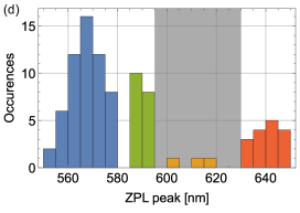
The variations in ZPL position cannot be explained alone by local strain in the crystal environment. The shifts caused by strain are too small to account for the variety of ZPLs35. Of particular note is that the ZPLs seem to bunch in groups around 560 nm18, 580 nm36, 640 nm13, 33 and 714 nm33. We define these as groups 1 through 4, respectively. It is believed that a different point-like defect is responsible for each group with the crystal lattice locally strained or changed otherwise, thus explaining the spread around these wavelengths. Shifts of the transition line caused by different isotopes would be much smaller than the emission linewidth. The vibronic bandshape of most defects is very similar, indicating that they have the same symmetry group. We note that there are occasional ZPLs falling into neither of these categories. It is likely that these originate from surface contaminants. Moreover, the bandshape of these differ from the bandshape typical for other emitters in the three groups, which supports this conjecture.
Using super-resolution techniques, these defects have been localized in 2D with sub-diffraction resolution37. The direct imaging on the atomic scale using high-resolution scanning transmission electron microscopy (STEM) is limited to a few layers, as the images contain information from all layers (essentially being a projection of all layers onto 2D). One way around this is to use a more advanced method like high-angle annular dark-field imaging (HAADF), with which it is possible to detect the presence of a vacancy within a few layers (maybe up to 3-5 layers). A vacancy would change the detected intensity by changing the scattering probability locally, and thus this would reveal such a defect with the exact location in the XY plane. However, this still does not contain any information about the Z direction. Recently, a method to correlate optical and electron characterizations of quantum emitters in very thin hBN was demonstrated31. This method, however, also yields no information about the Z direction. In addition, detecting the presence of a vacancy using HAADF cannot be used on thicker crystals, because the intensity contrast would be too low.
In this work, we localize the quantum emitters hosted by multilayer hBN in the third dimension with atomic precision. We develop deterministic layer-by-layer plasma etching of hBN. This way we can remove a single hBN monolayer at a time and check ex-situ when the defect disappears. We thereby measure the precise distance of the emitter from the surface of the host crystal. While this is a destructive technique, it allows us to extract the exact number of layers in which the defect was located. Repeating our experiment for many defects allows us to generate sufficient statistics. We also model photophysical properties theoretically with finite-difference time-domain simulations and density functional theory.
Results and Discussion
Layer-by-layer etching of hBN
Our approach to extract the location of the defects in the Z direction is to selectively remove one hBN monolayer at a time and check after each step, if the defect is still present. We first developed the layer-by-layer etching of hBN using an oxygen plasma. We note that similar etching of hBN on the atomic scale was reported recently using an argon plasma38. While this is an important milestone, however, Park et al. etched layers at a time and scaled this down to monolayer etching38. Nevertheless, with this technique as well as our method (see below), it is possible to fabricate large hBN monolayers. These are very difficult to obtain using mechanical exfoliation alone, due to the poor optical contrast of hBN, which has a zero-crossing in the visible spectrum39.
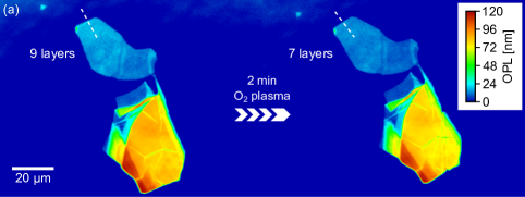
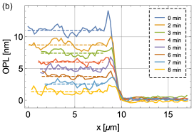
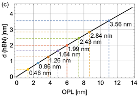
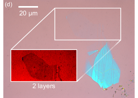
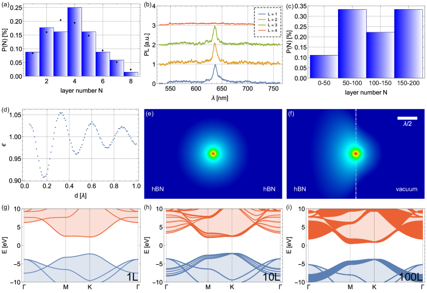
We mechanically exfoliated hexagonal boron nitride from bulk crystal onto a viscoelastic polymer. Thin, but still several nm thick hBN flakes were selected by optical contrast for dry transfer to a Si substrate terminated with a layer of thermally grown SiO2 (262 nm). For the etching we used an oxygen plasma generated from a microwave field and empirically optimized the plasma parameters (see Methods). The crystal thickness after each successive etching step is measured with a phase-shift interferometer (PSI), which is a much faster method than using an atomic force microscope (AFM) at the cost of a lower lateral resolution. Figure 1(a) shows the PSI image prior to any plasma treatment and after 2 min of etching time, where the crystal thickness decreased. The top flake consists of 9 and 7 atomic layers, respectively. The optical path length (OPL) difference between the substrate and the crystal (measured along the white dashed lines in Figure 1(a)) at a PSI wavelength of nm after each cumulative etching step is shown in Figure 1(b). It can be seen that the etched thickness is linear with time. The OPL can be converted to physical thickness using rigorous coupled-wave analysis (RCWA) simulations40, as shown in Figure 1(c). The simulations assume the refractive index of hBN to be 1.849, which was extracted by fitting an RCWA model to data pairs consisting of AFM and PSI measurements. It is worth noting that the relation between OPL and physical thickness is nonlinear for large OPLs. The data points in Figure 1(c) correspond to the PSI measurements (colored accordingly). Since the physical thickness of hBN is nm per layer41, we can extract that the crystal presented here was etched layer-by-layer from 9 layers to monolayer, with an etching rate of 1 layer per 63 s. A microscope image with an artificially-enhanced optical contrast of the bilayer is shown in Figure 1(d). At the optimized plasma conditions, this atomic layer-by-layer etching is highly reliable, with no fails (i.e. 0 or 2 layers etched) out of 31 runs. Moreover, we used the same technique on TMDs without failures and the method was also used for precise layer-by-layer thinning of black phosphorus42 or MoS243. Assuming the failure probability to be would reproduce our etching success of hBN with a high probability of 96.9. Deviating from the ideal plasma conditions (63 s etching time, for all details see Methods) results in process failures. This is evident by the fact that reducing the etching time by 10 s resulted into 2 out of 6 crystals not being etched and increasing the etching time by 10 s resulted in two layers being etched in 1 out of 3 cases (see Supporting Information, Figure S1). The reason why multiple layers can be etched without doubling the etching time is because it takes some time to start cracking the bonds, once that process starts, a faster etching rate can be achieved.
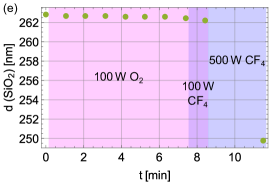
It is important to note that the plasma may damage the substrate. The OPL is dependent on the SiO2 thickness and the RCWA simulations assume this to be fixed. We checked the thickness of a SiO2 layer ex-situ after each etching step using variable angle spectroscopic ellipsometry (VASE). After 7 min at 100 W of cumulative plasma treatment, the thickness of a SiO2 layer decreased from 262.68(1) to 262.46(1) nm (see Figure 1(e)), so on average the SiO2 thinning is nm per step. According to the RCWA simulations such substrate thickness difference results in a change of the OPL much smaller than the resolution of the PSI (0.1 nm). Therefore, we can neglect this effect. This is, however, in general dependent on the type of plasma. For a comparison: using a CF4 plasma at 100 W for 1 min results in a thickness change of 0.22 nm of the SiO2 and using a CF4 plasma at 500 W for 3 min in the plasma field maximum (see Methods) etches 12.49 nm.
Creation of quantum emitters
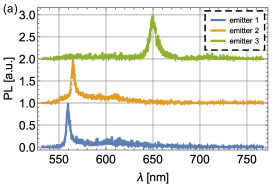
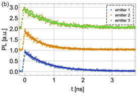
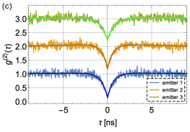
The fabrication of multilayer hBN flakes for hosting single-photon emitter is similar to the procedure above. After transfer to the substrate, the flakes are treated with an oxygen plasma at different conditions and successively annealed in a rapid thermal annealer18. To locate the defects each flake is scanned in a custom-built confocal micro-photoluminescence (PL) system with a resolution ranging from 0.2 or m. The pump laser, with its wavelength at 522 nm, is blocked by a long-pass filter and the emission is collected in-reflection. The defects almost exclusively occur at the edges of the host crystal flakes, due to a lower defect formation energy at these locations. Defects can, however, also form along crystal cracks within the flake. The defect formation energy there is lower as well. The spectra of three sample emitters are shown in Figure 2(a), which have their ZPLs at 559.78(7), 565.15(6) and 650.16(7) nm and Lorentzian linewidths of 2.24(10), 2.51(9) and 4.39(9) nm, respectively. All sample emitters presented here emit more than 80 of their photoluminescence (PL) into the ZPL, which allows for a high quantum efficiency. Time-resolved photoluminescence reveals a single-exponential decay of the excited state population for each defect with lifetimes 770(7), 549(7) and 794(13) ps, respectively (see Figure 2(b)). The excitation laser is pulsed at a repetition rate of 20.8 MHz and a pulse length of 300 fs. While this allows for high peak intensities, two-photon absorption of the band gap of hBN is still impossible, because . To prove that the localized exciton emits indeed non-classical light we utilize a Hanbury Brown and Twiss (HBT)-type interferometer, which allows for measuring the second order correlation function (see Figure 2(c)). We fit a three-level model with excited and meta-stable shelving state to our data. The correlation function is then given by
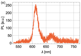
with the anti- and bunching-amplitudes , , and the characteristic lifetimes , . For the three sample emitters we find and , respectively. There was no background correction44 necessary due to the low detector noise compared to the single-photon brightness. This also means that the observed finite multi-photon probability is not caused by detector dark counts, but rather noise sources excited by the laser. Note that the experimental data was normalized such that for infinite time delay . As already mentioned, the literature reports ZPLs typically bunch around certain wavelengths. In fact, in our experiments we have seen this to happen around 560 nm, 590 nm and 640 nm, as the histogram in Figure 2(d) shows. With our fabrication method, however, we were not able to create emitters with ZPLs nm with statistical significance. In addition, sometimes we created an emitter not falling into any of the groups defined above. We believe that these are contaminating fluorescent molecules adsorbed onto the surface of hBN. Their emission is typically much weaker and their spectrum broader compared to the other emitters (see Figure 2(e)).
Atomic localization of quantum emitters
With 93 quantum emitters fabricated and characterized, we could utilize the atomic etching of hBN, removing one layer at a time. After each cumulative plasma etching step, the flakes were scanned again and we checked if the defect survived (see Supporting Information, Figure S2 for the process flow). It is possible that this etching creates new emitters, but at the layer-by-layer etching parameters, we expect the linear defect formation density to be m-1 (i.e. one defect forms on average per 50m crystal edge length)18. Thus, it is unlikely that an emitter is removed and at the same time a new one forms at the same location. In addition, as the photophysics of the defects vary substantially, it would be even more unlikely that a newly created emitter that formed at the location of a previous emitter has similar photophysical properties (in terms of e.g. ZPL, lifetime, and dipole orientation). In fact, we did see occasionally new defects appear at new locations, but they are not counted toward the statistics in this study. The histogram of the number layer after which the defect disappeared is shown in Figure 3(a). The best fit to any univariate distribution reveals a Poisson distribution with a mean of 3.8. This means that the emitters are very close to the surface.
When looking at how the photophysics evolve as the top layers are successively etched, it becomes clear that the emission is stable until the emitter is removed (see Figure 3(b)). The photoluminescence does not decrease gradually nor change its lineshape. Rather the PL from the defects disappears suddenly entirely, and for all upon removal. This means the quantum emitters are well isolated within one layer with no appreciable inter-layer interaction. In principle, it is possible the wave function of the trapped charge carrier is spread over multiple layers, thus the defect could enter a dark state even if some layers above the layer containing the chemical defect are etched (while the defect itself is not etched yet). There is, however, no further evidence supporting this conjecture. In addition, all the emitters with ZPLs falling not into one of the categories in the histogram in Figure 2(d) disappeared after the first etching step. This is evidence for the fact that these emitters are indeed surface contaminants. As expected, the Raman shift after each etching step remained constant, indicating that there is not much strain in the crystal, which would relax as the layers are etched.
The extracted layer number is believed to be highly accurate. Assuming a failure probability (see above) results in a success probability of 77.2 that all layer numbers are correct (in total there were 258 etching steps). However, as all samples were etched at the same time, there is a chance that if one process failed, many samples would be affected. A process fail could be that it took a longer time for the plasma to ignite or to stabilize the gases (both ignition and stabilization happens at a higher plasma power, which is subsequently regulated down to the set power), so to exclude this possibility the plasma parameters are recorded in-situ.
The results so far prove emitters (formed by oxygen plasma treatment) are always very close to the surface. This raises a few questions: (1) Why are the emitters close to the surface? (2) Are emitters always close to the surface, or does this depend on the defect formation method? (3) Is this an explanation for the shorter excited state lifetime of the plasma treated quantum emitters?
The dominant ion species in the plasma is O2+ (at lower pressure and higher power O+ becomes more dominant). The expected ion energy during the defect formation plasma treatment is eV. Unfortunately, this ion energy is too low for Monte Carlo methods like SRIM45, preventing an accurate calculation of the projected ion range in matter (in this case hBN). However, in our case the plasma treatment is a chemical and not physical process. This means the process is mostly limited to the crystal surface, as the ions have only low kinetic energy and cannot penetrate deep into the crystal. The kinetic energy of the ions is similar to the defect formation energy in hBN, which is on the order of a few eV46. Moreover, the O and O defect have formation energies of 5.19 and 2.20 eV, respectively, so they could easily be produced by the ions47. The oxygen radicals are highly reactive and are thus likely producing defects. It was recently pointed out, however, that it is unclear whether the defects are actually created using the plasma processing or one of the many other methods, or if preexisting, initially dark defects are activated via modification or restructuring of the crystal environment48. Both options are possible and our data so far does not allow to favor one over the other explanation.
While the oxygen plasma only acts onto the crystal surface, defect diffusion is also an important consideration. Without the exact knowledge of the chemical defect structure this is impossible to estimate, but at least a few things are known: First, hBN has strong sp2-hybridized covalent bonds, so the defect diffusion activation energy (that is the energy required to move along the reaction path) is rather large. It is expected that diffusion is predominantly in-plane and not inter-layer due to the direct in-plane bonds, so diffusion deep into the crystal is not likely. For hBN, due to the heteronuclear structure, defect diffusion is partially suppressed, as homonuclear B-B and N-N are energetically unfavorable (these homonuclear bonds are temporarily formed as the defects moves along the reaction path)49. This reduces e.g. vacancy migration compared to graphene. The diffusion activation energy calculated with DFT range from 2.6 to 6.0 eV at 0 K for vacancies and divacancies, with the structures often relaxing to their initial configuration49. This already shows the smaller defect diffusion. Furthermore, at the rapid annealing temperature of 850∘C (in this experiment), only the boron vacancy has a diffusion coefficient larger than 1 Å2s-149. Future calculations have to show how the diffusion of other point-like complexes scales. It is worth noting, that the result of the defect diffusion activation energy from DFT calculations shows a small dependency on the specifically used pseudopotential50.
To address the second question, we repeat the experiment with emitters fabricated with electron irradiation23, 24. The electron accelerating voltage was 10 kV with an electron fluence of cm-2. Given the thickness of the hBN flakes being m, the kinetic energy of the electrons is sufficient to fully transmit through the hBN crystals (see Supporting Information, Figure S3(a)). The energy loss of the electrons is dominated by collisions with the boron and nitrogen nuclei, as the radiative stopping power is much smaller at 10 keV kinetic electron energy (see Supporting Information, Figure S3(b)). Therefore, bremsstrahlung does not play any role. With the projected range of the electrons being 1.4m at keV, it is expected that emitters created or activated by electron irradiation are not exclusively near the crystal surface. Monte Carlo simulations of electron trajectories through the hBN crystal (see Supporting Information, Figure S3(c,d)) also confirm this. Repeating the atomic etching on these new emitters confirms this, as none of the emitters was found within the first ten layers, and the emitters being randomly positioned within the crystal. Etching at much larger steps (s of layers at a time, even though we note this was not calibrated sufficiently) shows that defects created by electron irradiation are formed throughout the crystal (see Figure 3(c)). More precisely, the emitters form not exclusively at the crystal edges or dislocations anymore, in agreement with previous experiments24. Interestingly, the excited state lifetime of these emitters is typically longer compared to the plasma etched ones, with lifetimes ranging from ns (see Supporting Information, Figure S4).
Theoretical modeling
Finally, we address the third question. Within the crystal, the photon density of states is decreased compared to vacuum. This is a Purcell-like effect, where the radiative lifetime is modified as the dielectric environment changes. The Purcell factor as a function of emitter distance to the surface is calculated using finite-difference time-domain (FDTD) simulations (see Methods) and shown is in Figure 3(d). The Purcell factor (and thus the excited state lifetime of an ideal dipole) oscillates and reaches 1 in the limit . In this limit there is no enhancement or suppression. It becomes clear that this effect only makes up a few percent in lifetime changes, so this alone cannot explain the shorter lifetime. It is still noteworthy, that there is enhancement very close to the surface, while deeper (nm) there is suppression. The electric field mode profiles in both limits show the emitter deep within hBN emits like an ideal dipole, while the emitter at the surface emits stronger into the crystal than into vacuum (see Figure 3(e,f)). This means the actual emitter brightness is even larger than experiments so far suggest. For emitters in cavities51, this does not matter, as both directions are captured by the cavity. As the different lifetime is not solely due to a Purcell-like effect, we use density functional theory calculations to investigate if surface states could be the cause for the shorter lifetime. We calculate the electronic band structure of hBN for one (1L), ten (10L), and 100 layers (100L) of hBN (see Figure 3(g-i)). The calculations show, that as more layers are added also more energy bands are added. Due to layer-layer interactions these bands spread, but there are no genuine isolated surface bands introduced into the band gap. This implies that, unless the defect levels are very close to one of the band edges, surface states do not influence the lifetime of the defect. Therefore, we conclude that the shorter defect lifetime in our experiments is likely due to interaction with surface defects introducing additional decay pathways, or with surface phonons making existing decay pathways faster.
Conclusions
In this work, we have developed deterministic atomically layer-by-layer etching of hBN with an oxygen plasma. This was utilized to destructively localize quantum emitters hosted by hBN. We found that emitters fabricated by a different plasma process are always very close to the surface, within a few layers, while emitters fabricated by intense electron irradiation are located throughout the entire crystal thickness. For both creation methods, emitters are more likely to form at flake edges and grain boundaries. It is notable that they also form away from these domains, in what appears to be undistorted crystal. Creation near the surface is a likely explanation for the shorter excited state lifetime hBN quantum emitters exhibit when fabricated by plasma etching. The emitter lifetime is influenced by additional decay pathways introduced by surface defects, or interactions with surface phonons making existing decay pathways faster. In contrast, emitters deep within the crystal have lifetimes times longer, as they are well isolated from the environment and surface effects.
Considering now the implications that our observations have for the identity of the quantum emitters. Our etching study is consistent with the confinement of the emitting defect to a single layer, as per past observation of the emitters in monolayer samples13. The creation of deep defects away from a boundary by electron irradiation is an important observation. It implies that the defect can be a product of radiation damage and so is further evidence that it involves a vacancy or interstitial. Specifically either a nitrogen vacancy V, a boron-vacancy V, an intralayer interstitial or an interlayer interstitial. To identify which, we need to interpret the effects of annealing.
At our annealing temperature of 850∘C, it is known that the V is mobile, whilst V is not. It is reasonable to expect that the interlayer interstitials are also mobile due to the low interlayer bond energies of the material. Upon annealing, we observe improved photostability and linewidth, but no significant change in the number of emitters18. We attribute the improved optical properties to the removal of interstitials and single V, which we expect to lead to an improved charge stability and reduced electrical noise since these defects likely act as donors or acceptors. If the density of the V created by the radiation is low, then our annealing observation would imply that the defect does not involve V. This is because if the defects were single V, then the number of emitters would decrease with annealing, and if it were a complex involving one or more V, then the number of emitters would increase until saturation of the other constituents of the complex (i.e. V or impurities). However, we are not necessarily drawing this conclusion here, since our intense electron irradiation may have rather created a very high density of V, which even without annealing, could have saturated the creation of emitters (i.e. by creating V in close proximity to V or an impurity). In this case, the defect may well involve V. Unfortunately, we cannot determine which V density limit our radiation produced because there is insufficient information about the V creation cross-section for electron radiation. Future work should focus on establishing the V density created before annealing and relating this to the creation / destruction / no change of emitters during annealing to establish whether or not V is involved in the defect.
The creation of the defects by the oxygen plasma may imply that the defect involves oxygen impurities through their incorporation at the surface. Generalizing this hypothesis to the creation of deep emitters by electron irradiation, this would imply that oxygen is also a deep impurity in our samples. This appears reasonable given that O may also form similar sp2 bonds as B and N if it can donate an electron to a nearby acceptor. Future work should seek to combine variation of oxygen impurity and radiation damage to ascertain whether the defect is indeed an O-V complex.
The results might also allow for a direct identification of the defect, as the knowledge of optically active defects very close to the surface might allow for imaging with high-resolution tunneling electron microscopes. A full understanding of the defect nature is required for tuning and engineering specific properties that will ultimately lead to a wider applicability in various scenarios.
Methods
Plasma etching
The oxygen plasma was generated from a microwave field (PVA TePla). Prior to any experiments, the plasma chamber was cleaned for 5 min at 500 W to remove any contaminants. We found the optimal single layer etching conditions empirically at a plasma power of 102 W for 63 s at a pressure of 0.332 mbar and a gas flow rate of 300 cm3/min (deviating from this by 10 decreases the success probability). All experiments were carried our at room temperature. The plasma time includes about s during which the plasma ignites and the gases are stabilized. The plasma field is highly anisotropic and varies across the plasma chamber. Thus, for repeatable results it is crucial to place the substrates always at the same position in the chamber. Unless stated otherwise, this position is at the plasma field minimum. It should be mentioned that the optimal parameters reported here depend on the specific gas pump, plasma generator and geometry of the chamber, which requires to optimize these parameters on every other system individually.
Fabrication and optical characterization
Thin flakes of hBN were mechanically exfoliated from bulk crystal (used as received from HQGraphene) to a viscoelastic stamp (Gel-Pak WF-40-X4) using the tape method. Crystals with thicknesses down to nm can be identified by optical contrast with a standard optical microscope and are subsequently transferred by dry contact to a Si substrate with a 262 nm thermally grown oxide layer. For the quantum emitters, we used crystals with thicknesses ranging from nm. The emitters were created during an oxygen plasma etching step at 200 W in the plasma field maximum and subsequently rapidly thermally annealed at 850C in an Ar atmosphere. The electron irradiated emitters have been fabricated using a scanning electron microscope in an FEI Helios 600 NanoLab, where the electrons were accelerated using a high voltage of 10 kV. The samples were irradiated with a fluence of cm-2, which was calculated with , where is the electron current, is the frame time, is the electron charge, and is the frame area. The irradiation took place at room temperature at a pressure mPa. For emitter localization, a custom-built PL setup was used which utilized an ultrashort-pulsed 522 nm laser with a pulse length of 300 fs at a repetition rate of 20.8 MHz. The laser was focused to the diffraction limit with a Olympus /0.9 dry objective and the samples were scanned using Newport translation stages with a spatial resolution up to 0.2m. The emission was collected in-reflection through the same objective and frequency-filtered using Semrock RazorEdge ultrasteep long-pass edge filters. The light is coupled via a grating to either a CCD or a single-photon avalanche diode (SPAD) from Micro Photon Devices allowing to extract the spectrum or the temporally and spectrally resolved photoluminescence. The correlation between excitation pulse and arrival time of the fluorescence photon is given by a PicoHarp 300. For measuring the second-order correlation function we utilize another diode laser at 512 nm and two SPADs.
Finite-difference time-domain simulations
The finite difference time-domain simulations were performed using Lumerical FDTD Solutions, a commercial grade simulator based on the FDTD method52. To calculate the Purcell enhancement and emitter dynamics, an in-plane dipole emitter at 560 nm was defined in the center within a slab of hBN, with a dielectric constant of 3.42 at 532 nm (this was obtained from experiments). The slab was thinned down from one direction (which is equivalent to moving the emitter to the surface) and the Purcell enhancement as well as the electric field mode profile was recorded for each crystal thickness. A dynamic mesh was chosen to capture all potential emitter dynamics. The simulations assume perfectly matched layer boundary conditions, which are reflectionless or absorbing boundaries, to account for the finite memory size.
Density functional theory calculations
The DFT calculations have been performed with QuantumATK with the Virtual NanoLab front end53, 54. QuantumATK utilizes numerical linear combination of atomic orbitals basis sets and the density matrix for closed or periodic systems is calculated by diagonalization of the Kohn-Sham Hamiltonian. Monolayer hBN crystals have been defined using a supercell containing two atoms and the geometry has been optimized using a Monkhorst-Pack reciprocal space grid. The optimization converged when all forces were below eV Å-1. The electron exchange-correlation was described with the Perdew-Burke-Ernzerhof (PBE) functional in the generalized gradient approximation55. For all atoms a double zeta polarized basis set was chosen and band structure was routed along high symmetry points. The ten- and 100-layer hBN crystals have been constructed in a similar way, with the lattice constant also geometrically optimized and the k-sampling in this direction chosen such that it does not influence the simulation results. {acknowledgement} This work was funded by the Australian Research Council (CE170100012, FL150100019, DE140100805, DP180103238, DE170100169). We thank the ACT Node of the Australian National Fabrication Facility for access to their nano- and microfabrication facilities. We also thank H. Tan for access to the TRPL system and C. Corr and F. Karouta for useful discussions about plasma processing.
References
- O’Brien et al. 2009 O’Brien, J. L.; Furusawa, A.; Vučković, J. Photonic quantum technologies. Nat. Photon. 2009, 3, 687–695
- Gisin et al. 2002 Gisin, N.; Ribordy, G.; Tittel, W.; Zbinden, H. Quantum cryptography. Rev. Mod. Phys. 2002, 74, 145–195
- Aspuru-Guzik and Walther 2012 Aspuru-Guzik, A.; Walther, P. Photonic quantum simulators. Nat. Phys. 2012, 8, 285–291
- Ladd et al. 2010 Ladd, T. D.; Jelezko, F.; Laflamme, R.; Nakamura, Y.; Monroe, C.; O’Brien, J. L. Quantum computers. Nature 2010, 464, 45–53
- Tonndorf et al. 2015 Tonndorf, P.; Schmidt, R.; Schneider, R.; Kern, J.; Buscema, M.; Steele, G. A.; Castellanos-Gomez, A.; van der Zant, H. S. J.; de Vasconcellos, S. M.; Bratschitsch, R. Single-photon emission from localized excitons in an atomically thin semiconductor. Optica 2015, 2, 347–352
- Srivastava et al. 2015 Srivastava, A.; Sidler, M.; Allain, A. V.; Lembke, D. S.; Kis, A.; Imamoǧlu, A. Optically active quantum dots in monolayer WSe2. Nat. Nanotechnol. 2015, 10, 491–496
- Koperski et al. 2015 Koperski, M.; Nogajewski, K.; Arora, A.; Cherkez, V.; Mallet, P.; Veuillen, J.-Y.; Marcus, J.; Kossacki, P.; Potemski, M. Single photon emitters in exfoliated WSe2 structures. Nat. Nanotechnol. 2015, 10, 503–506
- He et al. 2015 He, Y.-M.; Clark, G.; Schaibley, J. R.; He, Y.; Chen, M.-C.; Wei, Y.-J.; Ding, X.; Zhang, Q.; Yao, W.; Xu, X.; Lu, C.-Y.; Pan, J.-W. Single quantum emitters in monolayer semiconductors. Nat. Nanotechnol. 2015, 10, 497–502
- Chakraborty et al. 2015 Chakraborty, C.; Kinnischtzke, L.; Goodfellow, K. M.; Beams, R.; Vamivakas, A. N. Voltage-controlled quantum light from an atomically thin semiconductor. Nat. Nanotechnol. 2015, 10, 507–511
- Palacios-Berraquero et al. 2016 Palacios-Berraquero, C.; Barbone, M.; Kara, D. M.; Chen, X.; Goykhman, I.; Yoon, D.; Ott, A. K.; Beitner, J.; Watanabe, K.; Taniguchi, T.; Ferrari, A. C.; Atatüre, M. Atomically thin quantum light-emitting diodes. Nat. Commun. 2016, 7, 12978
- Branny et al. 2016 Branny, A.; Wang, G.; Kumar, S.; Robert, C.; Lassagne, B.; Marie, X.; Gerardot, B. D.; Urbaszek, B. Discrete quantum dot like emitters in monolayer MoSe2: Spatial mapping, magneto-optics, and charge tuning. Appl. Phys. Lett. 2016, 108, 142101
- Klein et al. 2019 Klein, J.; Lorke, M.; Florian, M.; Sigger, F.; Wierzbowski, J.; Cerne, J.; Müller, K.; Taniguchi, T.; Watanabe, K.; Wurstbauer, U.; Kaniber, M.; Knap, M.; Schmidt, R.; Finley, J. J.; Holleitner, A. W. Atomistic defect states as quantum emitters in monolayer MoS2. 2019, arXiv:1901.01042
- Tran et al. 2016 Tran, T. T.; Bray, K.; Ford, M. J.; Toth, M.; Aharonovich, I. Quantum emission from hexagonal boron nitride monolayers. Nat. Nanotechnol. 2016, 11, 37–41
- Tran et al. 2017 Tran, T. T.; Wang, D.; Xu, Z.-Q.; Yang, A.; Toth, M.; Odom, T. W.; Aharonovich, I. Deterministic Coupling of Quantum Emitters in 2D Materials to Plasmonic Nanocavity Arrays. Nano Lett. 2017, 17, 2634–2639
- Vogl et al. 2019 Vogl, T.; Sripathy, K.; Sharma, A.; Reddy, P.; Sullivan, J.; Machacek, J. R.; Zhang, L.; Karouta, F.; Buchler, B. C.; Doherty, M. W.; Lu, Y.; Lam, P. K. Radiation tolerance of two-dimensional material-based devices for space applications. 2019, 10, 1202
- Dietrich et al. 2018 Dietrich, A.; Bürk, M.; Steiger, E. S.; Antoniuk, L.; Tran, T. T.; Nguyen, M.; Aharonovich, I.; Jelezko, F.; Kubanek, A. Observation of Fourier transform limited lines in hexagonal boron nitride. Phys. Rev. B 2018, 98, 081414
- Kianinia et al. 2017 Kianinia, M.; Regan, B.; Tawfik, S. A.; Tran, T. T.; Ford, M. J.; Aharonovich, I.; Toth, M. Robust Solid-State Quantum System Operating at 800 K. ACS Photonics 2017, 4, 768–773
- Vogl et al. 2018 Vogl, T.; Campbell, G.; Buchler, B. C.; Lu, Y.; Lam, P. K. Fabrication and Deterministic Transfer of High-Quality Quantum Emitters in Hexagonal Boron Nitride. ACS Photonics 2018, 5, 2305–2312
- Schell et al. 2017 Schell, A. W.; Takashima, H.; Tran, T. T.; Aharonovich, I.; Takeuchi, S. Coupling Quantum Emitters in 2D Materials with Tapered Fibers. ACS Photonics 2017, 4, 761–767
- Vogl et al. 2017 Vogl, T.; Lu, Y.; Lam, P. K. Room temperature single photon source using fiber-integrated hexagonal boron nitride. J. Phys. D: Appl. Phys. 2017, 50, 295101
- Chejanovsky et al. 2016 Chejanovsky, N.; Rezai, M.; Paolucci, F.; Kim, Y.; Rendler, T.; Rouabeh, W.; Fávaro de Oliveira, F.; Herlinger, P.; Denisenko, A.; Yang, S.; Gerhardt, I.; Finkler, A.; Smet, J. H.; Wrachtrup, J. Structural Attributes and Photodynamics of Visible Spectrum Quantum Emitters in Hexagonal Boron Nitride. Nano Lett. 2016, 16, 7037–7045
- Xu et al. 2018 Xu, Z.-Q.; Elbadawi, C.; Tran, T. T.; Kianinia, M.; Li, X.; Liu, D.; Hoffman, T. B.; Nguyen, M.; Kim, S.; Edgar, J. H.; Wu, X.; Song, L.; Ali, S.; Ford, M.; Toth, M.; Aharonovich, I. Single photon emission from plasma treated 2D hexagonal boron nitride. Nanoscale 2018, 10, 7957–7965
- Choi et al. 2016 Choi, S.; Tran, T. T.; Elbadawi, C.; Lobo, C.; Wang, X.; Juodkazis, S.; Seniutinas, G.; Toth, M.; Aharonovich, I. Engineering and Localization of Quantum Emitters in Large Hexagonal Boron Nitride Layers. ACS Appl. Mater. Interfaces 2016, 8, 29642–29648
- Ngoc My Duong et al. 2018 Ngoc My Duong, H.; Nguyen, M. A. P.; Kianinia, M.; Ohshima, T.; Abe, H.; Watanabe, K.; Taniguchi, T.; Edgar, J. H.; Aharonovich, I.; Toth, M. Effects of High-Energy Electron Irradiation on Quantum Emitters in Hexagonal Boron Nitride. ACS Appl. Mater. Interfaces 2018, 10, 24886–24891
- Proscia et al. 2018 Proscia, N. V.; Shotan, Z.; Jayakumar, H.; Reddy, P.; Cohen, C.; Dollar, M.; Alkauskas, A.; Doherty, M.; Meriles, C. A.; Menon, V. M. Near-deterministic activation of room-temperature quantum emitters in hexagonal boron nitride. Optica 2018, 5, 1128–1134
- Tawfik et al. 2017 Tawfik, S. A.; Ali, S.; Fronzi, M.; Kianinia, M.; Tran, T. T.; Stampfl, C.; Aharonovich, I.; Toth, M.; Ford, M. J. First-principles investigation of quantum emission from hBN defects. Nanoscale 2017, 9, 13575–13582
- Abdi et al. 2018 Abdi, M.; Chou, J.-P.; Gali, A.; Plenio, M. B. Color Centers in Hexagonal Boron Nitride Monolayers: A Group Theory and Ab Initio Analysis. ACS Photonics 2018, 5, 1967–1976
- Sajid et al. 2018 Sajid, A.; Reimers, J. R.; Ford, M. J. Defect states in hexagonal boron nitride: Assignments of observed properties and prediction of properties relevant to quantum computation. Phys. Rev. B 2018, 97, 064101
- Reimers et al. 2018 Reimers, J. R.; Sajid, A.; Kobayashi, R.; Ford, M. J. Understanding and Calibrating Density-Functional-Theory Calculations Describing the Energy and Spectroscopy of Defect Sites in Hexagonal Boron Nitride. J. Chem. Theory Comput. 2018, 14, 1602–1613
- López-Morales et al. 2018 López-Morales, G. I.; Proscia, N. V.; López, G. E.; Meriles, C. A.; Menon, V. M. Toward the Identification of Atomic Defects in Hexagonal Boron Nitride: X-Ray Photoelectron Spectroscopy and First-Principles Calculations. 2018, arXiv:1811.05924
- Hayee et al. 2019 Hayee, F.; Yu, L.; Zhang, J. L.; Ciccarino, C. J.; Nguyen, M.; Marshall, A. F.; Aharonovich, I.; Vučković, J.; Narang, P.; Heinz, T. F.; Dionne, J. A. Correlated optical and electron microscopy reveal the role of multiple defect species and local strain on quantum emission. 2019, arXiv:1901.05952
- Bourrellier et al. 2016 Bourrellier, R.; Meuret, S.; Tararan, A.; Stéphan, O.; Kociak, M.; Tizei, L. H. G.; Zobelli, A. Bright UV Single Photon Emission at Point Defects in h-BN. Nano Lett. 2016, 16, 4317–4321
- Tran et al. 2016 Tran, T. T.; Elbadawi, C.; Totonjian, D.; Lobo, C. J.; Grosso, G.; Moon, H.; Englund, D. R.; Ford, M. J.; Aharonovich, I.; Toth, M. Robust Multicolor Single Photon Emission from Point Defects in Hexagonal Boron Nitride. ACS Nano 2016, 10, 7331–7338
- Shotan et al. 2016 Shotan, Z.; Jayakumar, H.; Considine, C. R.; Mackoit, M.; Fedder, H.; Wrachtrup, J.; Alkauskas, A.; Doherty, M. W.; Menon, V. M.; Meriles, C. A. Photoinduced Modification of Single-Photon Emitters in Hexagonal Boron Nitride. ACS Photonics 2016, 3, 2490–2496
- Grosso et al. 2017 Grosso, G.; Moon, H.; Lienhard, B.; Ali, S.; Efetov, D. K.; Furchi, M. M.; Jarillo-Herrero, P.; Ford, M. J.; Aharonovich, I.; Englund, D. Tunable and high-purity room temperature single-photon emission from atomic defects in hexagonal boron nitride. Nat. Commun. 2017, 8, 705
- Abidi et al. 2019 Abidi, I. H.; Mendelson, N.; Tran, T. T.; Tyagi, A.; Zhuang, M.; Weng, L.-T.; Ozyilmaz, B.; Aharonovich, I.; Toth, M.; Luo, Z. Selective Defect Formation in Hexagonal Boron Nitride. 2019, arXiv:1902.07932
- Kianinia et al. 2018 Kianinia, M.; Bradac, C.; Sontheimer, B.; Wang, F.; Tran, T. T.; Nguyen, M.; Kim, S.; Xu, Z.-Q.; Jin, D.; Schell, A. W.; Lobo, C. J.; Aharonovich, I.; Toth, M. All-optical control and super-resolution imaging of quantum emitters in layered materials. Nat. Commun. 2018, 9, 874
- Park et al. 2018 Park, H.; Shin, G. H.; Lee, K. J.; Choi, S.-Y. Atomic-scale etching of hexagonal boron nitride for device integration based on two-dimensional materials. Nanoscale 2018, 10, 15205–15212
- Gorbachev et al. 2011 Gorbachev, R. V.; Riaz, I.; Nair, R. R.; Jalil, R.; Britnell, L.; Belle, B. D.; Hill, E. W.; Novoselov, K. S.; Watanabe, K.; Taniguchi, T.; Geim, A. K.; Blake, P. Hunting for Monolayer Boron Nitride: Optical and Raman Signatures. Small 2011, 7, 465–468
- Yang et al. 2002 Yang, J.; Wang, Z.; Wang, F.; Xu, R.; Tao, J.; Zhang, S.; Qin, Q.; Luther-Davies, B.; Jagadisch, C.; Lu, Y. Atomically thin optical lenses and gratings. Light Sci. Appl. 2002, 5, e16046
- Li and Chen 2016 Li, L. H.; Chen, Y. Atomically Thin Boron Nitride: Unique Properties and Applications. Adv. Funct. Mater. 2016, 26, 2594–2608
- Pei et al. 2016 Pei, J.; Gai, X.; Yang, J.; Wang, X.; Yu, Z.; Choi, D.-Y.; Luther-Davies, B.; Lu, Y. Producing air-stable monolayers of phosphorene and their defect engineering. Nat. Commun. 2016, 7, 10450
- Xiao et al. 2016 Xiao, S.; Xiao, P.; Zhang, X.; Yan, D.; Gu, X.; Qin, F.; Ni, Z.; Han, Z. J.; Ostrikov, K. K. Atomic-layer soft plasma etching of MoS2. Sci. Rep. 2016, 6, 19945
- Beveratos et al. 2001 Beveratos, A.; Brouri, R.; Gacoin, T.; Poizat, J.-P.; Grangier, P. Nonclassical radiation from diamond nanocrystals. Phys. Rev. A 2001, 64, 061802
- Ziegler et al. 2010 Ziegler, J. F.; Ziegler, M.; Biersack, J. SRIM - The stopping and range of ions in matter. Nucl. Instr. Meth. Phys. Res. B 2010, 268, 1818–1823
- Huang and Lee 2012 Huang, B.; Lee, H. Defect and impurity properties of hexagonal boron nitride: A first-principles calculation. Phys. Rev. B 2012, 86, 245406
- McDougall et al. 2017 McDougall, N. L.; Partridge, J. G.; Nicholls, R. J.; Russo, S. P.; McCulloch, D. G. Influence of point defects on the near edge structure of hexagonal boron nitride. Phys. Rev. B 2017, 96, 144106
- Toth and Aharonovich 2019 Toth, M.; Aharonovich, I. Single Photon Sources in Atomically Thin Materials. Annu. Rev. Phys. Chem. 2019, 70, 123–142
- Zobelli et al. 2007 Zobelli, A.; Ewels, C. P.; Gloter, A.; Seifert, G. Vacancy migration in hexagonal boron nitride. Phys. Rev. B 2007, 75, 094104
- Estreicher et al. 2011 Estreicher, S. K.; Backlund, D. J.; Carbogno, C.; Scheffler, M. Activation Energies for Diffusion of Defects in Silicon: The Role of the Exchange-Correlation Functional. Angew. Chem. Int. Ed. 2011, 50, 10221–10225
- Vogl et al. 2019 Vogl, T.; Lecamwasam, R.; Buchler, B. C.; Lu, Y.; Lam, P. K. Space-compatible cavity-enhanced single-photon generation with hexagonal boron nitride. 2019, arXiv:1902.03019
- 52 Lumerical Solutions, Inc., https://www.lumerical.com/products/fdtd-solutions/
- Smidstrup et al. 2017 Smidstrup, S.; Stradi, D.; Wellendorff, J.; Khomyakov, P. A.; Vej-Hansen, U. G.; Lee, M.-E.; Ghosh, T.; Jónsson, E.; Jónsson, H.; Stokbro, K. First-principles Green’s-function method for surface calculations: A pseudopotential localized basis set approach. Phys. Rev. B 2017, 96, 195309
- 54 Synopsys QuantumATK, version 2016.3 with the Virtual NanoLab front end, https://www.synopsys.com/silicon/quantumatk.html
- Perdew et al. 1996 Perdew, J. P.; Burke, K.; Ernzerhof, M. Generalized Gradient Approximation Made Simple. Phys. Rev. Lett. 1996, 77, 3865–3868