In-situ strain tuning in hBN-encapsulated graphene electronic devices
Abstract
Using a simple setup to bend a flexible substrate, we demonstrate deterministic and reproducible in-situ strain tuning of graphene electronic devices. Central to this method is the full hBN encapsulation of graphene, which preserves the exceptional quality of pristine graphene for transport experiments. In addition, the on-substrate approach allows one to exploit strain effects in the full range of possible sample geometries and at the same time guarantees that changes in the gate capacitance remain negligible during the deformation process. We use Raman spectroscopy to spatially map the strain magnitude in devices with two different geometries and demonstrate the possibility to engineer a strain gradient, which is relevant for accessing the valley degree of freedom with pseudo-magnetic fields. Comparing the transport characteristics of a suspended device with those of an on-substrate device, we demonstrate that our new approach does not suffer from the ambiguities encountered in suspended devices.
The large mechanical strength of two-dimensional (2D) crystals allows one to modify their optical and electronic properties by externally induced strain fields Roldán et al. (2015). Graphene, one of the key examples of 2D materials, is of particular interest because of its peculiar electronic properties Castro Neto et al. (2009). A series of intriguing effects were predicted for strained graphene, such as the appearance of a scalar potential Guinea et al. (2010), pseudomagnetic fields Guinea et al. (2009, 2010); Zhu et al. (2015), valley filtering Milovanović and Peeters (2016); Yesilyurt et al. (2016) or superconductivity Uchoa and Barlas (2013). Different methods have been introduced to generate strain in graphene. One common approach is based on suspended graphene, where strain is induced by using different microactuators Pérez Garza et al. (2014); Downs et al. (2016); Goldsche et al. (2018); Colangelo et al. (2018) or by simply bending a flexible substrate Guan and Du (2017). In other approaches, graphene is not suspended and strain can be generated by bending a flexible substrate Mohiuddin et al. (2009), by using highly stressed metallic pads Shioya et al. (2015), or by placing graphene on periodic structures Jiang et al. (2017); Liu et al. (2018); Zhang et al. (2018). However, several challenges that need to be overcome simultaneously hampered the progress of these platforms for studying strain effects in transport experiments. First, complex fabrication usually significantly degrades the graphene quality and hinders the observation of the strain effects. In addition, the device is often limited to very basic structures, without the possibility of local gating or multi-terminal devices. Second, mechanical deformations often result in changes in the gate capacitance that cannot be easily distinguished from the actual strain effects. The third challenge is that the strain should be in-situ tunable and non-hysteretic to disentangle strain effects from other effects.


Here we report a straining method that meets all the above requirements. Instead of suspending the graphene, we encapsulate the graphene with hexagonal boron-nitride (hBN) and directly strain the van der Waals (vdW) heterostructure on-substrate. This approach preserves the exceptional quality of pristine graphene, which is a significant advantage for transport experiments. We use Raman spectroscopy to demonstrate that our method is versatile and that it allows one to engineer various strain fields, such as strain gradients, which are important for the generation of pseudo-magnetic fields Guinea et al. (2010). We also show that the edge contacts work reliably and can sustain a strain up to %. In the first low-temperature electron transport measurements, we demonstrate that our method solves the problem of an artificial gating effect due to the bending-induced change in the graphene-to-gate distance, which is present in suspended graphene devices. Therefore, our approach of on-substrate encapsulated graphene offers an ideal platform for studying strain effects in transport experiments.
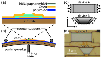
As shown schematically in Figure 1a, we fabricate hBN-encapsulated graphene devices with edge contacts Wang et al. (2013) and an electrical bottom gate on a polyimide coated flexible substrate. Bending this substrate in a three-point bending setup, as illustrated in Figure 1b, generates a strain field in the graphene. The deformation of the substrate is determined by the displacement z of the pushing-wedge relative to the mounting position. The hBN encapsulation ensures the high quality of the graphene, and the metallic contacts and the gate allow us to perform transport experiments while tuning the strain in-situ. The metallic contacts are essential for generating strain in a vdW heterostructure. In the Supporting Information Figure S2, we present a comparison between devices with and without contacts. The result shows that strain cannot be induced by substrate bending in devices without contacts. Based on the assumption that the graphene sheet is pulled uniaxially by the contacts during the bending of the substrate, we designed devices with two different geometries in order to obtain different strain fields. This is illustrated in Fig. 1c, where the rectangle (device A) is expected to result in a homogeneous strain field, while the trapezoid (device B) should exhibit a strain gradient along the y-axis, i.e. perpendicular to the straining axis. An optical micrograph of two fabricated devices is shown in Fig. 1d.

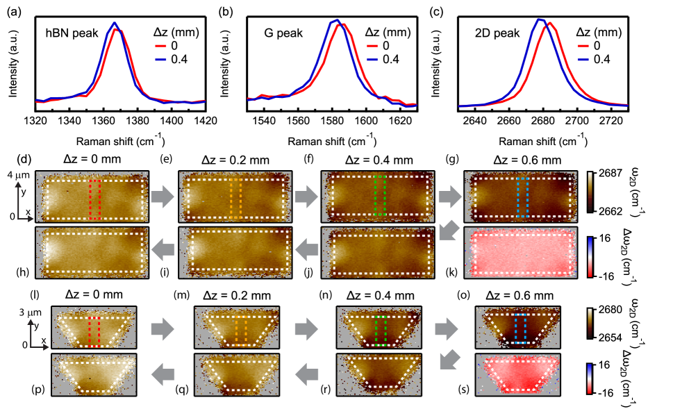
To characterize the strain fields for different displacements z, we perform Raman spectroscopy directly on a 3-point bending setup at room temperature. Previous studies reported characteristic redshifts in the Raman peaks of graphene Mohiuddin et al. (2009); Yoon et al. (2011); Frank et al. (2011), which we now use to quantify the local strain generated in these two devices. Typical Raman spectra of the hBN peak and the graphene G and 2D peaks are shown in Figures 2a-c, respectively, for two different z values. The bending of the substrate results in a redshift of all peaks, with the most prominent effect on the graphene 2D peak. For small strain values the 2D peak can be fitted by a single Lorentzian with center frequency Mohiuddin et al. (2009). In the following, we use spatially resolved Raman spectroscopy to map the strain field based on the redshift of the graphene 2D peak. The same analysis for the hBN Raman peak is presented in the Supporting Information Figure S4, which shows that both hBN and graphene are strained similarly in this method.
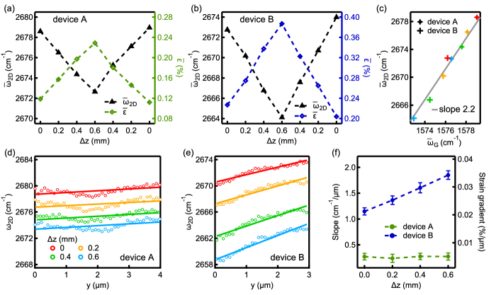
We first focus on the investigation of the rectangular device A. In Figures 2d-j, is plotted as a function of position for device A, for a series of increasing z from to (straining) and then decreasing back to (relaxing), as indicated by the gray arrows. With increasing z, shifts to lower values at all positions on the map, consistent with increasing strain everywhere in the graphene sheet. When z is decreased back to , reverts back to the initial values. The mean value averaged over the whole device is plotted as a function of z in Figure 3a, where z is first increased from to then decreased back to . The very symmetric V-shape reveals a linear dependence and a good reproducibility of the strain tuning in the graphene device and exhibits no significant hysteresis. The corresponding average strain values () are shown on the right axis, which are calculated using Mohr et al. (2009) with for unstrained graphene. We note that the former value is not known very accurately and our choice is among the intermediate reported values Mohiuddin et al. (2009); Mohr et al. (2009); Huang et al. (2010); Yoon et al. (2011); Frank et al. (2011); Polyzos et al. (2015); Colangelo et al. (2018). The latter value is obtained as the average over 10 Raman spectra measured at different positions on three different hBN/graphene/hBN stacks before fabrication. The strain values at z = are not 0, probably due to the intrinsic strain accumulated in the device after fabrication. We obtain an average strain of up to % and a maximum strain near the contacts of % for device A at z = . Figure 3c shows the plot of versus (center frequency of the graphene G peak) of both devices for different z values. The data points fall on a line of slope 2.2, which confirms strain as the origin of the redshift of the Raman peaks Lee et al. (2012); Neumann et al. (2015); Mueller et al. (2017); Goldsche et al. (2018).
We note that there is a small inhomogeneity in the map of for device A in Figure 2d which does not change significantly with external straining. We analyze the data in the scatter plot of versus in the Supporting Information Figure S3, which shows that the inhomogeneity in the maps of originates mostly from the strain variation over the large device area Lee et al. (2012); Neumann et al. (2015); Froehlicher and Berciaud (2015); Mueller et al. (2017). The homogeneity of the externally induced strain field can be seen directly in figure 2k, which shows a map of the change in the Raman shift, , between the map at z = (Figure 2g) and the map without external straining (Figure 2d). For this rectangular geometry, the externally induced strain is fairly homogeneous in the bulk with a vanishing strain gradient, which matches quite well the expected strain fields for device A as shown in Figure 1c. The detailed strain pattern for this geometry from finite element method (FEM) simulations is shown in Supporting Information Figure S5.
We now turn to the investigation of strain and strain gradients in the trapezoidal device B. The spatially resolved maps of for device B are plotted in Figure 2l-r for the same series of z as above for sample A. Also this device shows a tunable average strain controlled by z. The device averaged and the corresponding extracted strain values are plotted in Figure 3b as a function of z. At identical z value, the average strain for device B is larger than that for device A due to the smaller size of device B, but shows similar V-shape, i.e. a linear, non-hysteretic dependence on z. These findings can also be seen directly in the Raman maps. We obtain an average strain of up to % and maximum values at the lower sample edge of % for device B at z = . The existence of a strain gradient is visible in Figure 2m-o. At the shorter (bottom) edge of the device, shows a stronger shift than that at the longer (top) edge, which matches the predicted strain pattern for a trapezoidal geometry, as illustrated in Figure 1c (see also the FEM simulations in Supporting Information Figure S5). Figure 2s shows the difference between the Raman signals at large bending (Figure 2o) and no bending (Figure 2l).
To demonstrate the deterministic generation of a strain gradient in more detail, we plot for both devices in Figure 3d & e as a function of the position along the y-axis in the center of the device area, averaged over in the x-direction, as indicated by the colored dashed boxes in Figures 2d-g & l-o. For both devices we find a clear increase in the average strain (overall shift of the curves) and an essentially unchanged background variation with increasing z. In addition, for the trapezoidal geometry (device B) we find a clear linear increase in the strain when moving from the longer to the shorter sample edge.

We now take the average slope of these curves as an estimate of the large scale (non-microscopic) strain gradient along the y-axis. For this purpose we plot in Figure 3f the slopes of linear fits to the data in Figure 3d (device A) and Figure 3e (device B) as a function of z, with the right axis showing the corresponding extracted strain gradient. The small non-zero slope for device A stems from the small intrinsic strain variation over the large device area discussed above and stays constant for increasing z. In contrast, for device B we find a linear dependence of the average slope on the z, demonstrating that strain gradients can be generated by modifying the device geometry. The pseudo-magnetic field, , depends on the strain gradients, Guinea et al. (2009, 2010), with the Grüneisen parameter Pereira et al. (2009) and the interatomic distance. To estimate , we use and obtain values on the order of in the bulk of device B at z = .. We note that much larger strain gradients occur near the corners of the device which might result in pseudo-magnetic fields over locally. We also point out that larger average strain values can be achieved in this setup (see Supporting Information Figure S6), but with an increased probability of device failure, which happens at a strain on the order of .
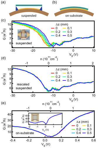
One of the major advantages of our technique is that the edge contacts not only act as clamps for the mechanical deformation, but allow for simultaneous transport experiments. Here we report first low-temperature () transport experiments with in-situ strain tuning of a device fabricated in the described fashion and compare the results to similar measurements on a device where the encapsulated graphene is suspended, using the LOR based suspension technique Tombros et al. (2011); Maurand et al. (2014). The two experiments are shown schematically in Figure 4a & b. For both devices the two-terminal differential conductance, , is measured as a function of the gate voltage, , for different z values, see Figures 4c & e, respectively.
There are significant differences between suspended and on-substrate devices for bending experiments. For the suspended device one can immediately find a systematic change of the curves in gate voltage with increasing z (see Figure 4c), while such an obvious effect is absent for the on-substrate device (see Figure 4e). The effects found in the suspended device can be fully accounted for by the change in the graphene-to-gate distance when bending the substrate, as depicted in Figure 4a. This is illustrated in Figure 4d, where we plot the data of Figure 4c rescaled linearly in gate voltage for each curve with as a fix point. This can be understood in a simple capacitor model in which the charge induced in the graphene are given by , with the effective capacitance between the graphene layer and the gate. If the capacitance is changed by a factor to due to the substrate bending, the same charge is induced at , which is equivalent to a rescaling in the gate voltage. This scaling factor is extracted for each curve by matching the CNP to that of the curve at z = and it is linear in z. After rescaling, all data points fall onto the same curve, see Fig. 4d. This demonstrates that the bending-induced gating effect is dominant for the suspended graphene device, which makes it very difficult to study effects due to actual strain.
This effect is absent in the on-substrate devices optimized for strain tuning. For comparison, we performed the same type of measurements also on an on-substrate device, with the results shown in Figure 4e. Since the gate voltage lever arm in this device is much larger than that for the suspended device due to the shorter graphene-to-gate distance, we apply smaller gate voltages to obtain a similar carrier density range as that in the data of the suspended device (see top axes of Figure 4d & e). The electron mobility of is extracted from a linear fit around the CNP, suggesting a high graphene quality in our device. On this gate voltage scale and also on much larger scale (see inset of Figure 4e), all curves with different z values are virtually identical, which demonstrates that there are no bending-induced changes in the carrier density or in the contact resistance in this experimental configuration. The additional conductance minimum at comes from a double moiré superlattice effect in encapsulated graphene Wang et al. (2019). We point out that on this scale of graphene straining we could not detect significant changes in the conductance.
In conclusion, we have successfully generated tunable and reversible strain fields in encapsulated graphene devices. Since these devices are fabricated on-substrates, i.e. not suspended, it allows us to design a large variety of device geometries. As an example, we use spatially resolved Raman imaging to demonstrate that the edge contact clamping and rectangular geometry result in a fairly homogeneous straining of the graphene. In a second step, we use this design freedom to generate a strain gradient in a trapezoidal geometry. In first transport experiments we then demonstrate another major advantage of on-substrate encapsulated devices, namely that the bending-induced gate capacitance change can be avoided, which is crucial for studying strain effects in transport experiments. This approach is not limited to graphene, but also suitable for studying strain effects in other 2D materials and complex vdW heterostructures, for example in MoS2 Conley et al. (2013); He et al. (2013); Zhu et al. (2013). Because our method is simple and intuitive, nonetheless allowing complex device structures, we expect that it will pave the way towards deterministic strain engineering and new approaches to valleytronics.
.1 Author contributions
L.W. fabricated the devices, performed the measurements and did the data analysis. S.Z. initiated the idea of hBN-encapsulation. A.B. did the FEM simulations. P.M and J.O. helped to develop the straining method. P.M., S.Z. and J.O. supported the device fabrication. A.B., P.M. and S.Z. helped with the data analysis. K.W. and T.T. provided high-quality hBN. C.S. initiated and supervised the project. L.W. and A.B. wrote the paper. All authors discussed the results and worked on the manuscript. All data in this publication are available in numerical form at DOI:10.5281/zenodo.2636531.
Acknowledgement
This work has received funding from the Swiss Nanoscience Institute (SNI), the ERC project TopSupra (787414), the European Union Horizon 2020 research and innovation programme under grant agreement No. 785219 (Graphene Flagship), the Swiss National Science Foundation, the Swiss NCCR QSIT, Topograph, ISpinText FlagERA network and from the OTKA FK-123894 grants. P.M. acknowledges support from the Bolyai Fellowship, the Marie Curie grant and the National Research, Development and Innovation Fund of Hungary within the Quantum Technology National Excellence Program (Project Nr. 2017-1.2.1-NKP-2017-00001). Growth of hexagonal boron nitride crystals was supported by the Elemental Strategy Initiative conducted by the MEXT, Japan and the CREST (JPMJCR15F3), JST. The authors thank Oliver Braun, David Indolese and Peter Rickhaus for fruitful discussions, and Sascha Martin and his team for their technical support.
References
- Roldán et al. (2015) R. Roldán, A. Castellanos-Gomez, E. Cappelluti, and F. Guinea, Journal of Physics: Condensed Matter 27, 313201 (2015).
- Castro Neto et al. (2009) A. H. Castro Neto, F. Guinea, N. M. R. Peres, K. S. Novoselov, and A. K. Geim, Rev. Mod. Phys. 81, 109 (2009).
- Guinea et al. (2010) F. Guinea, A. K. Geim, M. I. Katsnelson, and K. S. Novoselov, Phys. Rev. B 81, 035408 (2010).
- Guinea et al. (2009) F. Guinea, M. I. Katsnelson, and A. K. Geim, Nature Physics 6, 30 (2009).
- Zhu et al. (2015) S. Zhu, J. A. Stroscio, and T. Li, Phys. Rev. Lett. 115, 245501 (2015).
- Milovanović and Peeters (2016) S. P. Milovanović and F. M. Peeters, Applied Physics Letters 109, 203108 (2016).
- Yesilyurt et al. (2016) C. Yesilyurt, S. Ghee Tan, G. Liang, and M. B. A. Jalil, AIP Advances 6, 056303 (2016).
- Uchoa and Barlas (2013) B. Uchoa and Y. Barlas, Phys. Rev. Lett. 111, 046604 (2013).
- Pérez Garza et al. (2014) H. H. Pérez Garza, E. W. Kievit, G. F. Schneider, and U. Staufer, Nano Lett. 14, 4107 (2014).
- Downs et al. (2016) C. S. C. Downs, A. Usher, and J. Martin, Journal of Applied Physics 119, 194305 (2016).
- Goldsche et al. (2018) M. Goldsche, J. Sonntag, T. Khodkov, G. J. Verbiest, S. Reichardt, C. Neumann, T. Ouaj, N. von den Driesch, D. Buca, and C. Stampfer, Nano Lett. 18, 1707 (2018).
- Colangelo et al. (2018) F. Colangelo, A. Pitanti, V. Mišeikis, C. Coletti, P. Pingue, D. Pisignano, F. Beltram, A. Tredicucci, and S. Roddaro, 2D Materials 5, 045032 (2018).
- Guan and Du (2017) F. Guan and X. Du, Nano Lett. 17, 7009 (2017).
- Mohiuddin et al. (2009) T. M. G. Mohiuddin, A. Lombardo, R. R. Nair, A. Bonetti, G. Savini, R. Jalil, N. Bonini, D. M. Basko, C. Galiotis, N. Marzari, K. S. Novoselov, A. K. Geim, and A. C. Ferrari, Phys. Rev. B 79, 205433 (2009).
- Shioya et al. (2015) H. Shioya, S. Russo, M. Yamamoto, M. F. Craciun, and S. Tarucha, Nano Lett. 15, 7943 (2015).
- Jiang et al. (2017) Y. Jiang, J. Mao, J. Duan, X. Lai, K. Watanabe, T. Taniguchi, and E. Y. Andrei, Nano Lett. 17, 2839 (2017).
- Liu et al. (2018) Y. Liu, J. N. B. Rodrigues, Y. Z. Luo, L. Li, A. Carvalho, M. Yang, E. Laksono, J. Lu, Y. Bao, H. Xu, S. J. R. Tan, Z. Qiu, C. H. Sow, Y. P. Feng, A. H. C. Neto, S. Adam, J. Lu, and K. P. Loh, Nature Nanotechnology 13, 828 (2018).
- Zhang et al. (2018) Y. Zhang, M. Heiranian, B. Janicek, Z. Budrikis, S. Zapperi, P. Y. Huang, H. T. Johnson, N. R. Aluru, J. W. Lyding, and N. Mason, Nano Lett. 18, 2098 (2018).
- Wang et al. (2013) L. Wang, I. Meric, P. Y. Huang, Q. Gao, Y. Gao, H. Tran, T. Taniguchi, K. Watanabe, L. M. Campos, D. A. Muller, J. Guo, P. Kim, J. Hone, K. L. Shepard, and C. R. Dean, Science 342, 614 (2013).
- Yoon et al. (2011) D. Yoon, Y.-W. Son, and H. Cheong, Phys. Rev. Lett. 106, 155502 (2011).
- Frank et al. (2011) O. Frank, M. Mohr, J. Maultzsch, C. Thomsen, I. Riaz, R. Jalil, K. S. Novoselov, G. Tsoukleri, J. Parthenios, K. Papagelis, L. Kavan, and C. Galiotis, ACS Nano 5, 2231 (2011).
- Mohr et al. (2009) M. Mohr, K. Papagelis, J. Maultzsch, and C. Thomsen, Phys. Rev. B 80, 205410 (2009).
- Huang et al. (2010) M. Huang, H. Yan, T. F. Heinz, and J. Hone, Nano Lett. 10, 4074 (2010).
- Polyzos et al. (2015) I. Polyzos, M. Bianchi, L. Rizzi, E. N. Koukaras, J. Parthenios, K. Papagelis, R. Sordan, and C. Galiotis, Nanoscale 7, 13033 (2015).
- Lee et al. (2012) J. E. Lee, G. Ahn, J. Shim, Y. S. Lee, and S. Ryu, Nature Communications 3, 1024 (2012).
- Neumann et al. (2015) C. Neumann, S. Reichardt, P. Venezuela, M. Drögeler, L. Banszerus, M. Schmitz, K. Watanabe, T. Taniguchi, F. Mauri, B. Beschoten, S. V. Rotkin, and C. Stampfer, Nature Communications 6, 8429 (2015).
- Mueller et al. (2017) N. S. Mueller, S. Heeg, M. P. Alvarez, P. Kusch, S. Wasserroth, N. Clark, F. Schedin, J. Parthenios, K. Papagelis, C. Galiotis, M. Kalbáč, A. Vijayaraghavan, U. Huebner, R. Gorbachev, O. Frank, and S. Reich, 2D Materials 5, 015016 (2017).
- Froehlicher and Berciaud (2015) G. Froehlicher and S. Berciaud, Phys. Rev. B 91, 205413 (2015).
- Pereira et al. (2009) V. M. Pereira, A. H. Castro Neto, and N. M. R. Peres, Phys. Rev. B 80, 045401 (2009).
- Tombros et al. (2011) N. Tombros, A. Veligura, J. Junesch, J. Jasper van den Berg, P. J. Zomer, M. Wojtaszek, I. J. Vera Marun, H. T. Jonkman, and B. J. van Wees, Journal of Applied Physics 109, 093702 (2011).
- Maurand et al. (2014) R. Maurand, P. Rickhaus, P. Makk, S. Hess, E. Tóvári, C. Handschin, M. Weiss, and C. Schönenberger, Carbon 79, 486 (2014).
- Wang et al. (2019) L. Wang, S. Zihlmann, M.-H. Liu, P. Makk, K. Watanabe, T. Taniguchi, A. Baumgartner, and C. Schönenberger, Nano Lett. 19, 2371 (2019).
- Conley et al. (2013) H. J. Conley, B. Wang, J. I. Ziegler, R. F. Haglund, S. T. Pantelides, and K. I. Bolotin, Nano Lett. 13, 3626 (2013).
- He et al. (2013) K. He, C. Poole, K. F. Mak, and J. Shan, Nano Lett. 13, 2931 (2013).
- Zhu et al. (2013) C. R. Zhu, G. Wang, B. L. Liu, X. Marie, X. F. Qiao, X. Zhang, X. X. Wu, H. Fan, P. H. Tan, T. Amand, and B. Urbaszek, Phys. Rev. B 88, 121301 (2013).