Ultra-Strong Light-Matter Coupling in Deeply Subwavelength THz LC resonators
Abstract
The ultra-strong light-matter coupling regime has been demonstrated in a novel three-dimensional inductor-capacitor (LC) circuit resonator, embedding a semiconductor two-dimensional electron gas in the capacitive part. The fundamental resonance of the LC circuit interacts with the intersubband plasmon excitation of the electron gas at THz with a normalized coupling strength . Light matter interaction is driven by the quasi-static electric field in the capacitors, and takes place in a highly subwavelength effective volume . This enables the observation of the ultra-strong light-matter coupling with electrons only. Notably, our fabrication protocol can be applied to the integration of a semiconductor region into arbitrary nano-engineered three dimensional meta-atoms. This circuit architecture can be considered the building block of metamaterials for ultra-low dark current detectors.
Metamaterials were introduced to enable new electromagnetic properties of matter which are not naturally found in nature. Celebrated examples of such achievements are, for instance, negative refraction Shelby (2001) and artificial magnetism.Pendry et al. (1999) The unit cells of metamaterials are artificially designed meta-atoms that have dimensions ideally much smaller than the wavelength of interest .Cai and Šalaev (2010) Such meta-atoms act as high frequency inductor-capacitor (LC) resonators which sustain a resonance close to .Cai and Šalaev (2010) The resonant behaviour, occurring into highly subwavelength volumes, generates high electromagnetic field intensities which, as pointed out by the seminal paper of Pendry et al., Pendry et al. (1999) are crucial to implement artificial electromagnetic properties of a macroscopic ensemble of meta-atoms. Moreover, the ability to control and enhance the electromagnetic field at the nanoscale is beneficial for optoelectronic devices, such as nano-lasers Wang et al. (2017) electromagnetic sensors Chen et al. (2012); Belacel et al. (2017); Alves et al. (2018) and detectors. Shrekenhamer et al. (2012); Viti et al. (2014); Luxmoore et al. (2016); Palaferri et al. (2016, 2018) For instance, metamaterial architectures have lead to a substantial decrease of the thermally excited dark current in quantum infrared detectors, resulting in higher temperature operation. Palaferri et al. (2016, 2018)
The LC circuit can be seen as a quantum harmonic oscillator sustaining vacuum electric field fluctuations that scale as , where is the effective volume of the capacitive parts. Louisell (1990) For an emitter/absorber inserted between the capacitor plates, the light-matter interaction is proportional to , and thus strongly enhanced. Fundamental electro-dynamical phenomena, such as the Purcell effectPurcell et al. (1946) and strong light-matter coupling regimeYamamoto et al. (2000) can therefore be observed. In the strong coupling regime, energy is reversibly exchanged between the matter excitation and the electromagnetic resonator at the Rabi frequency . This results in an energy splitting of the circuit resonance into two polaritons states separated by . The regime of strong coupling has been observed in many physical systems which have been reviewed e.g. in Refs. 16; 17; 18, and some specific realizations with metamaterial resonators were achieved in the sub-THz, Scalari et al. (2012) THzTodorov et al. (2010a); Strupiechonski et al. (2012); Dietze et al. (2013) and the Mid-IRBenz et al. (2015); Askenazi et al. (2014, 2017) part of the spectrum. In these systems, the highly subwavelength interaction volumes combined with the collective effect of identical electronic transitions result into high coupling constants , and allow reaching the ultra-strong coupling regime where the Rabi splitting becomes of the same order of magnitude as the frequency of the material excitation , . Ciuti et al. (2005) Since there is virtually no lower limit for the interaction volume in LC resonators, the fascinating regime of ultra-strong coupling can be realized in structures having few electrons only. Todorov and Sirtori (2014); Keller et al. (2017) In such limit, the effective bosonization procedure employed to describe the properties of the two-dimensional electron gas breaks down, and one can investigate the unique regime where the few electrons in the system have to be exactly treated as fermions.Todorov and Sirtori (2014)
Recently, the ultra-strong coupling regime with a small number of electrons has been experimentally observed by coupling transitions between Landau levels in a two dimensional electron gas under a high magnetic field and nanogap complementary bow-tie antennas, with a record low number of 80 electrons.Keller et al. (2017) Those studies were performed in the sub-THz part of the spectrum (300GHz) using resonators based on a planar geometry. Here, we demonstrate a three-dimensional metamaterial architecture that has the potential to go beyond this limit in the THz range (3THz), without the need for a magnetic field. Our metamaterial allows confining the electric field in all directions of space into nanoscale volumes, on the order of . The resonance of the structure is coupled to an intersubband (ISB) transition of high density electron gas in the ground state of semiconductor quantum wells (QWs). A relative Rabi frequency of is attained with a record low overall number of electrons for intersubband systems. Other reports on coupled LC resonators-ISB transitions systems in the THz spectral range reached similar coupling constants of with a much greater mode volume and electron number ( and ).Paulillo et al. (2016) Comparable number of coupled electrons have been reported in the MIR spectral rangeBenz et al. (2013); Malerba et al. (2016) using very small mode volume cavities with , but at the expense of reducing the coupling constant ( in Ref. 30 and in Ref. 31). We use the dependence of the polariton splitting on the effective mode volume as a near field probe to estimate the highly subwavelength volume of our resonators in comparison with reference microcavity systems. Todorov et al. (2010a); Feuillet-Palma et al. (2012) These results are obtained thanks to a novel fabrication process that allows structuring metal patterns on both sides of a very thin semiconductor layer, which opens many degrees of freedom in the design and functionalization of 3D metamaterial architectures into optoelectronic devices.
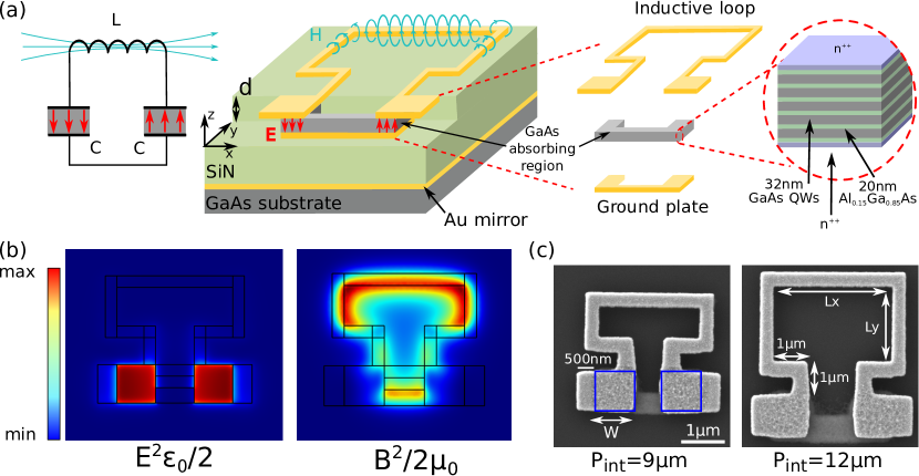
Our THz LC resonator is introduced in Fig. 1 (a), along with a sketch of the equivalent circuit. The bottom metallic ground plate is formed by two square capacitor plates of width , connected by a thin stripe. The top metallic part is composed of two rectangular capacitor plates (m) connected by a bent wire. Two parallel plate capacitors are thus formed at the overlap between the metallic pads, while the bent wire acts as an inductive loop. Note that the top metal plates are 500 nm wider than the bottom one, resulting in a 500 nm wide extension over the outer parts of the capacitor, as shown in Fig. 1 (c). The capacitors area is shown by the blue squares on the left image of this panel. The small extensions allow engineering the fringing fields between the two capacitor plates. By breaking the symmetry of the in-plane component of the electric field, they allow efficient coupling between the resonator mode and far-field radiation, as determined by previous work on SiN-based resonators. Mottaghizadeh et al. (2017) The circuit-like mode of the structure which oscillates at the lowest frequency confines the electric field in the capacitive areas while the magnetic field loops around the inductive wire, Todorov et al. (2015); Mottaghizadeh et al. (2017) as shown in Fig. 1 (b), calculated using finite-elements method simulations. They represent the electric (left) and the magnetic (right) energy density in the center plane of the resonator. The matter resonance is provided by GaAs/AlGaAs QWs inserted inside the capacitive elements. Note that the -component of the electric field is the only active component for ISB absorption. The resonator mode described above thus naturally fulfills the ISB polarization selection rule, which requires the electric field to be oriented along the growth axis of the QWs.
To fabricate the LC resonator, the ground plate is first patterned using e-beam lithography and used as a mask to etch the absorbing region with an inductively-coupled plasma. The structure is then encapsulated in a 3 m thick SiN layer, and the surface of the sample is metalized with an optically thick Au layer. The latter serves as a mirror which blocks the transmission into the substrate, such as the reflected beam contains only the spectral features of the metamaterial array. The sample (grown on a GaAs substrate) is then flipped and transferred to a host substrate using an epoxy, and the growth substrate is selectively etched away, revealing the bottom of the patterned absorbing region. The top inductive loop and rectangular capacitor plates are then defined using e-beam lithography. Figure 1 (c) shows scanning electron microscope images of typical LC resonators. In the following, we keep the lateral size of the capacitor m. The internal perimeter Pm of the inductive loop is varied from 9 to 14m to tune the resonant frequency across the 2-6 THz spectral region, as explained further. A single resonator fits in a square with a diagonal of 4.2 m (Pint=9 m) to 7 m (Pint=12 m), much smaller than the vacuum wavelength =100 m. The footprint of a single resonator ranges from to 55 m2, e.g. to .
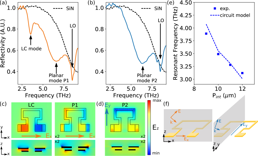
We first probe the optical properties of our system at room temperature, where the ISB absorption can be neglected as the thermal energy is sufficiently high to equally populate the first few energy levels of the QWs, and we can study the electromagnetic modes of the resonator alone. Todorov et al. (2012) We perform reflectivity experiments using a dry-air purged Fourier Transform Spectrometer (FTIR) (Brucker Vertex 70v) and a globar source. The FTIR is equipped with a custom made reflectivity setup, which allows focusing the globar beam on the sample with the help of a pair of F1 parabolic mirrors, and the reflected beam is measured with a He cooled Ge bolometer (QMC Instruments). Light is linearly polarized and impinging at 45° on the sample, as sketched in Fig. 2 (f). To ensure good spatial overlap with the globar beam, we fabricate dense arrays composed of 50 000 resonators separated by 2 m from each other, with a total area of 22 mm2. All spectra are normalized by the reference from a Au mirror. In Fig. 2 (a)-(b) we show typical spectra obtained for resonators with P m, with light polarized respectively along the line formed by the capacitors (), and orthogonally to that line (). By comparing the two spectra, we first note the presence of a dip in the reflectivity spectrum for -polarized light at 3.5 THz, which is absent in the -polarized spectrum. This corresponds to the LC mode of the resonator represented in Fig.1. A broad resonance is observed in both polarizations at 6.5 THz, whose origin will be discussed later. A strong dip is observed just above 8 THz in both polarizations. This corresponds to the lower frequency edge of the GaAs reststrahlen band arising from the optical phonons,Kittel (1996) confirming the very strong localization of the electric field in the semi-conductor layer enabled by our device, as the GaAs only constitutes 3.5% of the surface probed by the THz beam. The baseline in all spectra arises from the 3 m thick SiN layer, as confirmed by the reflectivity spectra from an area without any patterns (dashed curves in Fig. 2 (a)-(b)). Indeed the SiN layer has a residual absorption in this spectral region.Cataldo et al. (2012)
To clarify the origin of the various resonances observed in the experiments we simulated the reflectivity of the structure using a commercial finite element method software (Comsol v.5.3a). Maps of the component of the electric field for the three modes are shown in Figs. 2 (c)-(d) in two cut planes located at the center of the capacitors. Note that in the right panel of Fig. 2 (c) and in Fig. 2 (d) the magnitude of the electric field has been multiplied by two for clarity. The -plane color maps show the expected electric field distribution for the LC mode, and reveal that the resonance at 6.5 THz actually corresponds to two different modes (P1 and P2) excited with different polarizations ( and respectively). Comparing the -plane maps, we see that only the LC mode efficiently confines the electric field inside the capacitors. P1 and P2 are modes where the electric field lies mainly in the plane of the inductive loop, reminiscent of the modes observed in planar metamaterial resonators.Zhou et al. (2007) Notably, simulations including the top loop alone (and not the ground plate) show the same P1 and P2 modes but not the three-dimensional LC resonance. These two modes couple to the isotropic phonon absorption in the GaAs regions below the Au pads, as they still have a spectral overlap with the GaAs reststrahlen band. A detailed survey of the different modes sustained by the structure is beyond the scope of this paper, and from now on we will restrict the analysis to the LC mode, which is the only one providing electric field almost exclusively localized in the capacitive parts and satisfying the selection rule for the QW ISB absorption.
The LC resonance is tuned by changing the internal perimeter Pint of the inductive loop, while keeping the capacitance parts fixed. The resonant frequencies as a function of Pint are reported in Fig. 2 (e) (symbols). We compare the experimental results with those of a lumped element model which corresponds to the equivalent circuit sketched in Fig. 1(a) (see Supplementary Materials for more information). The resonant frequencies of the model, provided by are plotted in dashed lines in Fig. 2 (c), and are in good agreement with those extracted from the measurements. The calculated inductance varies from pH to pH. The calculated capacitance is aF, which compares well with the value for an ideal parallel plate capacitor aF, with and the material and vacuum permittivities. The difference between these two values can be explained by the contribution of the fringing fields and of the in-plane parasitic gap capacitance between the two metal pads. This evidences that the fundamental mode of our resonators operates in the near quasi-static limit.
To explore the ultra-strong light-matter coupling regime, we have inserted in our resonators an absorbing region consisting of 5 repetitions of 32nm GaAs quantum wells separated by 20nm Al0.15Ga0.85As barriers, similar to the design described in Ref. 20; 35. The QWs are modulation-doped by Si -doped regions placed 5 nm away from the QW, with a nominal sheet carrier density of cm-2. In such thin double-metal structures the presence of the two metal-semiconductor interfaces creates a depletion layer on each side of the semiconductor region, bending the conduction band profile and usually depleting 2-3 QWs.Sze and Kwok (2006); Todorov et al. (2012) To compensate for this effect, we introduced a doped AlGaAs spacing layer and a doped GaAs external layer (both doped at cm-3) on each side of the absorbing region, which is of total thickness nm. Additional details on the band structure and sample design are provided in the Supplementary materials. The matter excitation coupled to the LC resonator is an intersubband plasmon of frequency , where is the bare ISB transition frequency and is the plasma frequency of the two-dimensional electron gas in the QWs.Ando et al. (1982) The latter is provided by the expression , where is the electron charge, is the electron effective mass in the QW, (resp. ) is the surface electron density in the first (second) subband, and is an effective length of the quantum well as defined in Ref. 41. The quantity can be seen as an effective thickness of the quantum confined electron plasma and depends on the wave functions of the first and second subbands (see Ref. 41). We find nm, smaller than the physical thickness of the QW (32 nm). For the following discussion, it is important to note that and hence depend on the charge density in a single quantum well only. The characteristic equation of the coupled intersubband plasmon-resonator system is written in the general case:
| (1) |
where is the resonator frequency, is the transition oscillator strength ( for an infinite QW), describes the filling factor of the QWs inside the absorbing region with charged quantum wells, and describes the optical overlap of the resonator mode with the absorbing region, which is related to the effective mode volume as explained further. Note that the coefficient quantifies the filling factor of the QWs inside the absorbing region that takes into account the fact that the active dipoles are not homogeneously distributed in the semiconductor, but are only localized inside the QWs. Instead, the dimensionless overlap factor represents the fraction of electromagnetic energy coupled into the -component of the electric field and spatially overlapping with the semiconductor layers inside the capacitor. It is defined by:Zanotto et al. (2012)
| (2) |
where the energy stored in the vertical component of the electric field (the sole component of the field to couple to ISB transitions) is integrated over the absorbing region (AR) volume and normalized by the total electric energy of the mode. The effective mode volume is then determined by the relation . Since this definition accounts for field leakage outside the capacitive parts of the resonator. Eq. 1 provides the upper (UP) and lower (LP) polariton frequencies as a function of . The minimum splitting between UP and LP is exactly the vacuum Rabi splitting :
| (3) |
The Rabi splitting can also be expressed as , where is the total number of electrons populating the subband . The Rabi splitting that is experimentally determined from spectroscopic studies, as described further, is thus directly linked to the effective mode volume which is an important quantity in nano-photonic systems.Liu et al. (2016) However, the analysis of our experimental data is easier to perform with the help of Eq. (3). Ultimately, two parameters govern the maximum coupling strength: the overlap factor and the number of available dipoles in the microcavity volume . The strength of the coupling can thus be controlled by tuning the population difference through the change of the temperature of the sample.
In order to asses the parameters and in our LC resonators, we compare the spectroscopic features of the ultra-strong coupling regime in the LC resonators with square patch double-metal microcavities. Such double-metal cavities sustain a resonance at , where is the size of the patch, and the effective index of the confined mode.Todorov et al. (2010b) They have been shown to reach the ultra-strong coupling regime with similar absorbing regions with , however with a much larger effective mode volume. Todorov et al. (2010a, 2012) They will serve as a reference to our current LC samples.Feuillet-Palma et al. (2012)
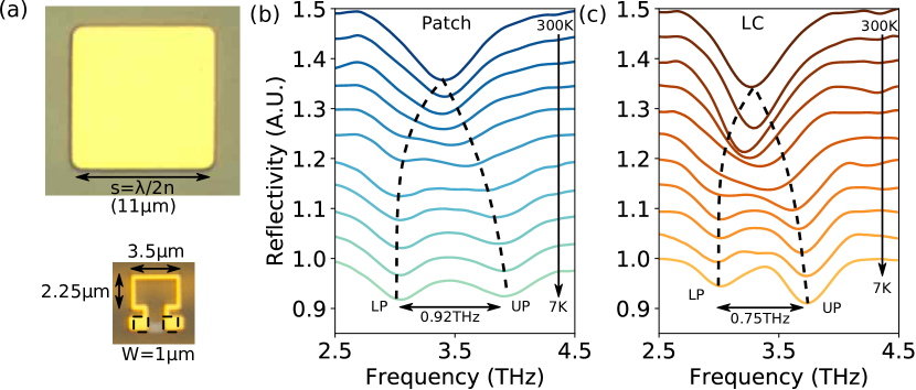
A comparison between a LC resonator and a patch cavity with the same absorbing region is shown in Fig. 3. Optical microscope images of the two types of resonators, which have identical resonant frequencies (3.5 THz) are shown in Fig. 3 (a) (to scale). While the size of the patch cavity is set by the diffraction limit, clearly the lateral confinement of the electric field in the capacitors of the LC resonator is well below that limit. For spectroscopic studies at cryogenic temperatures, the samples are mounted on the cold finger of a liquid helium continuous flow cryostat, and probed in a reflectivity experiment. We report in Fig. 3 (b) (resp. (c)) the reflectivity of the patch cavities array (resp. LC resonator) tuned near the intersubband plasmon resonance as a function of temperature, ranging from 300 K to 7 K. In the case of the LC resonator, the baseline induced by the SiN has been removed for clarity. In both cases the room temperature spectra show a single resonance around 3.5 THz as the population difference between the first two subbands is zero (), owing to the thermal electron distribution. The matter excitation thus vanishes, and one only sees the LC and the patch cavity resonances. This single resonance splits when decreasing the temperature as the population difference increases, and the maximum separation is obtained at low temperature (7K), reaching 0.92 THz for the patch cavities and 0.75 THz for the LC resonators.
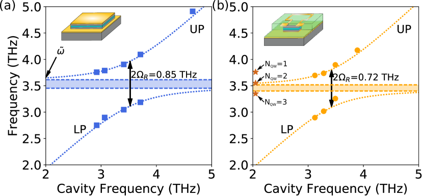
Tuning the LC and patch resonant frequencies allows us to more precisely map the dispersion relation given in equation (1). In Fig. 4 the position of the UP and LP modes at T=7 K are plotted as a function of the cavity frequency, obtained by modifying either the size of the patch cavities, or the inductance of the LC resonators through the internal perimeter Pint. We observe a clear anticrossing and the opening of a polaritonic gap between the two polariton branches. By fitting the data with equation (1), we can extract the Rabi splittings THz and THz, representing respectively 21% and 24% of the intersubband plasmon frequency determined from the fit of the dispersion relation. The slight reduction of the Rabi splitting for LC resonators can be due to both lateral depletion of the QW, as well as to the overlap factor that is less than unity.
We now want to determine separately the total charge and the overlap factor in our systems. We start by deducing the total charge left in the 5 QW patch cavity sample, by comparing it to a reference sample having exactly the same QWs, but repeated 25 times. The 25 QWs sample is also processed into patch cavities (Refs. 20; 35), and we can safely assume that . The data for that sample are provided in the Supplementary Materials, along with a detailed derivation of the method to extract the electronic population. We deduce that 21 QWs are populated, with an equivalent doping of cm-2. Using equation (3), (see also Ref. 20; 35) a proportionality rule yields the total surface charge density at low temperature:
| (4) |
In that case , and we find an equivalent total charge density of , meaning that only of the total charge is left is the QWs, confirming the importance of the depletion effects at the metal-semiconductor interfaces. Furthermore, for both samples we observe the same matter excitation frequency , which means the surface charge density per quantum well is the same. We therefore conclude that we have 2 charged quantum wells in the 5QW absorbing region. A more detailed analysis is given in the Supplementary Information.
Having determined the total charge in the case of the patch cavities, we use the same proportionality rule to compare the 5QW patch and LC resonators. We first assume that we have the same total charge in both samples. Then, according to equation (4) we can derive the geometric overlap factor . Comparing the data from Fig. 4 we derive a confinement factor . A more careful comparison of Fig. 4 (a) and (b) shows that the fits of the dispersion relations yields a plasmon frequency at a slightly lower frequency for the LC resonators (3.55 THz) than the one of the patch cavities (3.65 THz). Since the plasmon frequency is related to the plasma frequency through the formula , we conclude that the red shift is due to a lower plasma frequency of the LC as compared to the patch cavity. This is due to a further lateral depletion of the QWs originating from surface traps at the etched surface of the absorbing region, as already reported in the case of etched pillar or nanowire structures. Dietze et al. (2013); Amanti et al. (2013); Lähnemann et al. (2017) From our data, we infer a plasma frequency for the LC resonators that is 7.6% lower than the one for the patch cavities. Correcting for this effect yields an overlap factor . This value is slightly larger than the one predicted in numerical simulations, . The effective mode volume of the LC resonators is thus determined to be , almost two orders of magnitude smaller than the patch cavities. The low value of the effective mode volume is a striking feature of our resonator, since achieving an effective volume very close to the physical volume of the semiconductor absorbing region () represents a critical trade-off in double-metal geometries, owing to the leakage of the electric energy in fringing fields. Square or wire patch cavities indeed lead to factors close to unity at the expense of a large mode volume, while other systems report very small mode volume, sacrificing the overlap factor down to a few percents. Malerba et al. (2016); Paulillo et al. (2016) We can also estimate the intersubband plasmon frequency in the case where one or three QWs would be populated. The detail of the calculation is given in Supplementary Information, and the results are shown in stars in Fig. 4 (b). We can see that the intersubband plasmon frequencies obtained in the two cases strongly differ from our measurement, confirming the analysis presented above.
From the knowledge of the equivalent surface charge density we can deduce the total number of electrons participating in the coupling with the cavity and resonator modes. The calculation yields e-/patch and e-/capacitor. Our newly developed LC resonators thus allow us to greatly decrease the number of electrons involved in the coupling while maintaining a large vacuum Rabi splitting, making a step towards the few electrons regime beyond previous results on double-metal cavities. Feuillet-Palma et al. (2012); Paulillo et al. (2016); Malerba et al. (2016)
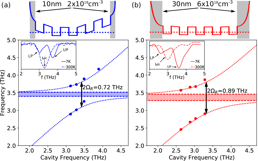
In order to improve further the strength of the light-matter coupling, we designed a second sample with an identical absorbing region, but with an increased thickness of the cavity (320 nm) and and increased doping density in the outermost GaAs layers ( cm-3). After processing into patch cavities and LC metamaterials, we perform the same experiments as described above (see Supplementary materials for details). Our results show that in the present sample, all 5 QWs are populated. This means that thanks to the increased charge density in the interface layers, the populated QWs participating in the optical absorption occupy a larger fraction of the total cavity volume, increasing the filling factor . However, we deduce a lower value of the optical overlap factor, =0.56, meaning a slightly higher effective volume than that of the previous LC sample. This could be explained by a partial screening of the penetration of the electric field inside the capacitors, owing to the higher number of free carriers in the contact layers. Nevertheless, as shown in Fig. 5, the Rabi splitting is increased to 0.89 THz in the new LC sample, reaching values of 0.27 of the ISB plasmon frequency. The total electron number is e-/capacitor. Remarkably, this value is one of the lowest achieved so far using ISB transitions coupled to metamaterials, while retaining a large ratio.
In conclusion, we demonstrate a deeply subwavelength confinement of electromagnetic energy with an effective mode volume and a reduction of the number of interacting electrons, down to a few thousands while keeping . The electron number is an order of magnitude larger than that recently reported in systems exploring the coupling between Landau level transitions and planar metamaterials.Keller et al. (2017) However, our structures will allow further reduction of the number of electrons while maintaining a large ratio . This can be achieved by reducing the size of the capacitive elements to a few hundreds of nanometers in our LC resonators. For instance, by maintaining a surface equivalent doping of cm-2 and working with a single quantum well, we could achieve ultra-strong light-matter coupling with only 10 electrons in 100 nm wide capacitors. Devices with such small capacitive elements have already been fabricated in SiN-based LC resonators.Mottaghizadeh et al. (2017)
An important asset of our device architectures is that they naturally provide the possibility to implement DC current input/output from the semiconductor region. Indeed, the top and bottom metallic parts are direct current uncoupled, and contacts can be taken directly on the inductive parts without hindering the sub-wavelength confinement in the capacitors. Such device architectures will allow us to study new effects related to the ultra-strong coupling, beyond the spectroscopic studies performed so far,Keller et al. (2017) such as polariton-assisted fermionic transport.Feist and Garcia-Vidal (2015); Orgiu et al. (2015); Bruhat et al. (2016); Stockklauser et al. (2017); Paravicini-Bagliani et al. (2018); Hagenmüller et al. (2018) The reduced number of electrons leads to a reduced number of dark states, optimizing the coupling between the collective electronic excitation and the electronic current.De Liberato and Ciuti (2009) Furthermore, in the weak coupling regime, these device architectures can be very beneficial for ultra-low dark current ISB detectors.Palaferri et al. (2016)
Acknowledgements.
The authors acknowledge the help of the technical staff from the cleanroom facility of Université Paris Diderot. We thank Li Chen for the wafer bonding of the samples used to fabricate patch antennas. This work was supported by the French National Research Agency under the contract ANR-16-CE24-0020. We acknowledge support from the EPSRC (UK) programme grant HyperTerahertz EP/P021859/1. EHL acknowledges support from the Royal Society and the Wolfson Foundation.References
- Shelby (2001) R. A. Shelby, Science 292, 77 (2001).
- Pendry et al. (1999) J. Pendry, A. Holden, D. Robbins, and W. Stewart, IEEE Transactions on Microwave Theory and Techniques 47, 2075 (Nov./1999).
- Cai and Šalaev (2010) W. Cai and V. M. Šalaev, Optical Metamaterials: Fundamentals and Applications (Springer, New York, NY, 2010) oCLC: 837215261.
- Wang et al. (2017) S. Wang, X.-Y. Wang, B. Li, H.-Z. Chen, Y.-L. Wang, L. Dai, R. F. Oulton, and R.-M. Ma, Nature Communications 8, 1889 (2017).
- Chen et al. (2012) T. Chen, S. Li, and H. Sun, Sensors 12, 2742 (2012).
- Belacel et al. (2017) C. Belacel, Y. Todorov, S. Barbieri, D. Gacemi, I. Favero, and C. Sirtori, Nature Communications 8, 1578 (2017).
- Alves et al. (2018) F. Alves, L. Pimental, D. Grbovic, and G. Karunasiri, Scientific Reports 8, 12466 (2018).
- Shrekenhamer et al. (2012) D. Shrekenhamer, W. Xu, S. Venkatesh, D. Schurig, S. Sonkusale, and W. J. Padilla, Physical Review Letters 109, 177401 (2012).
- Viti et al. (2014) L. Viti, D. Coquillat, D. Ercolani, L. Sorba, W. Knap, and M. S. Vitiello, Optics Express 22, 8996 (2014).
- Luxmoore et al. (2016) I. J. Luxmoore, P. Q. Liu, P. Li, J. Faist, and G. R. Nash, ACS Photonics 3, 936 (2016).
- Palaferri et al. (2016) D. Palaferri, Y. Todorov, A. Mottaghizadeh, G. Frucci, G. Biasiol, and C. Sirtori, New Journal of Physics 18, 113016 (2016).
- Palaferri et al. (2018) D. Palaferri, Y. Todorov, A. Bigioli, A. Mottaghizadeh, D. Gacemi, A. Calabrese, A. Vasanelli, L. Li, A. G. Davies, E. H. Linfield, F. Kapsalidis, M. Beck, J. Faist, and C. Sirtori, Nature 556, 85 (2018).
- Louisell (1990) W. H. Louisell, Quantum Statistical Properties of Radiation, Wiley Classics Library (Wiley, New York, 1990) oCLC: 833244245.
- Purcell et al. (1946) E. M. Purcell, H. C. Torrey, and R. V. Pound, Physical Review 69, 37 (1946).
- Yamamoto et al. (2000) Y. Yamamoto, F. Tassone, and H. Cao, Semiconductor Cavity Quantum Electrodynamics, springer ed. (2000).
- Baranov et al. (2018) D. G. Baranov, M. Wersäll, J. Cuadra, T. J. Antosiewicz, and T. Shegai, ACS Photonics 5, 24 (2018).
- Frisk Kockum et al. (2019) A. Frisk Kockum, A. Miranowicz, S. De Liberato, S. Savasta, and F. Nori, Nature Reviews Physics 1, 19 (2019).
- Forn-Díaz et al. (2018) P. Forn-Díaz, L. Lamata, E. Rico, J. Kono, and E. Solano, arXiv:1804:09275 (2018).
- Scalari et al. (2012) G. Scalari, C. Maissen, D. Turcinkova, D. Hagenmuller, S. De Liberato, C. Ciuti, C. Reichl, D. Schuh, W. Wegscheider, M. Beck, and J. Faist, Science 335, 1323 (2012).
- Todorov et al. (2010a) Y. Todorov, A. M. Andrews, R. Colombelli, S. De Liberato, C. Ciuti, P. Klang, G. Strasser, and C. Sirtori, Physical Review Letters 105, 196402 (2010a).
- Strupiechonski et al. (2012) E. Strupiechonski, G. Xu, M. Brekenfeld, Y. Todorov, N. Isac, A. M. Andrews, P. Klang, C. Sirtori, G. Strasser, A. Degiron, and R. Colombelli, Applied Physics Letters 100, 131113 (2012).
- Dietze et al. (2013) D. Dietze, A. M. Andrews, P. Klang, G. Strasser, K. Unterrainer, and J. Darmo, Applied Physics Letters 103, 201106 (2013).
- Benz et al. (2015) A. Benz, S. Campione, J. F. Klem, M. B. Sinclair, and I. Brener, Nano Letters 15, 1959 (2015).
- Askenazi et al. (2014) B. Askenazi, A. Vasanelli, A. Delteil, Y. Todorov, L. C. Andreani, G. Beaudoin, I. Sagnes, and C. Sirtori, New Journal of Physics 16, 043029 (2014).
- Askenazi et al. (2017) B. Askenazi, A. Vasanelli, Y. Todorov, E. Sakat, J.-J. Greffet, G. Beaudoin, I. Sagnes, and C. Sirtori, ACS Photonics 4, 2550 (2017).
- Ciuti et al. (2005) C. Ciuti, G. Bastard, and I. Carusotto, Physical Review B 72, 115303 (2005).
- Todorov and Sirtori (2014) Y. Todorov and C. Sirtori, Physical Review X 4, 041031 (2014).
- Keller et al. (2017) J. Keller, G. Scalari, S. Cibella, C. Maissen, F. Appugliese, E. Giovine, R. Leoni, M. Beck, and J. Faist, Nano Letters 17, 7410 (2017).
- Paulillo et al. (2016) B. Paulillo, J.-M. Manceau, L. H. Li, A. G. Davies, E. H. Linfield, and R. Colombelli, Applied Physics Letters 108, 101101 (2016).
- Benz et al. (2013) A. Benz, S. Campione, S. Liu, I. Montaño, J. Klem, A. Allerman, J. Wendt, M. Sinclair, F. Capolino, and I. Brener, Nature Communications 4 (2013), 10.1038/ncomms3882.
- Malerba et al. (2016) M. Malerba, T. Ongarello, B. Paulillo, J.-M. Manceau, G. Beaudoin, I. Sagnes, F. De Angelis, and R. Colombelli, Applied Physics Letters 109, 021111 (2016).
- Feuillet-Palma et al. (2012) C. Feuillet-Palma, Y. Todorov, R. Steed, A. Vasanelli, G. Biasiol, L. Sorba, and C. Sirtori, Optics Express 20, 29121 (2012).
- Mottaghizadeh et al. (2017) A. Mottaghizadeh, Y. Todorov, M. Cameau, D. Gacemi, A. Vasanelli, and C. Sirtori, Optics Express 25, 28718 (2017).
- Todorov et al. (2015) Y. Todorov, P. Desfonds, C. Belacel, L. Becerra, and C. Sirtori, Optics Express 23, 16838 (2015).
- Todorov et al. (2012) Y. Todorov, L. Tosetto, A. Delteil, A. Vasanelli, C. Sirtori, A. M. Andrews, and G. Strasser, Physical Review B 86, 125314 (2012).
- Kittel (1996) C. Kittel, Introduction to Solid State Physics, john wiley & sons ed. (1996).
- Cataldo et al. (2012) G. Cataldo, J. A. Beall, H.-M. Cho, B. McAndrew, M. D. Niemack, and E. J. Wollack, Optics Letters 37, 4200 (2012).
- Zhou et al. (2007) J. Zhou, T. Koschny, and C. M. Soukoulis, Optics Express 15, 17881 (2007).
- Sze and Kwok (2006) S. M. Sze and K. N. Kwok, Physics of Semiconductor Devices, john wiley & sons ed. (2006).
- Ando et al. (1982) T. Ando, A. B. Fowler, and F. Stern, Reviews of Modern Physics 54, 437 (1982).
- Todorov and Sirtori (2012) Y. Todorov and C. Sirtori, Physical Review B 85, 045304 (2012).
- Zanotto et al. (2012) S. Zanotto, R. Degl’Innocenti, L. Sorba, A. Tredicucci, and G. Biasiol, Physical Review B 85, 035307 (2012).
- Liu et al. (2016) K. Liu, S. Sun, A. Majumdar, and V. J. Sorger, Scientific Reports 6 (2016), 10.1038/srep37419.
- Todorov et al. (2010b) Y. Todorov, L. Tosetto, J. Teissier, A. M. Andrews, P. Klang, R. Colombelli, I. Sagnes, G. Strasser, and C. Sirtori, Optics Express 18, 13886 (2010b).
- Amanti et al. (2013) M. I. Amanti, A. Bismuto, M. Beck, L. Isa, K. Kumar, E. Reimhult, and J. Faist, Optics Express 21, 10917 (2013).
- Lähnemann et al. (2017) J. Lähnemann, A. Ajay, M. I. Den Hertog, and E. Monroy, Nano Letters 17, 6954 (2017).
- Feist and Garcia-Vidal (2015) J. Feist and F. J. Garcia-Vidal, Physical Review Letters 114 (2015), 10.1103/PhysRevLett.114.196402.
- Orgiu et al. (2015) E. Orgiu, J. George, J. A. Hutchison, E. Devaux, J. F. Dayen, B. Doudin, F. Stellacci, C. Genet, J. Schachenmayer, C. Genes, G. Pupillo, P. Samorì, and T. W. Ebbesen, Nature Materials 14, 1123 (2015).
- Bruhat et al. (2016) L. E. Bruhat, J. J. Viennot, M. C. Dartiailh, M. M. Desjardins, T. Kontos, and A. Cottet, Physical Review X 6, 021014 (2016).
- Stockklauser et al. (2017) A. Stockklauser, P. Scarlino, J. V. Koski, S. Gasparinetti, C. K. Andersen, C. Reichl, W. Wegscheider, T. Ihn, K. Ensslin, and A. Wallraff, Physical Review X 7, 011030 (2017).
- Paravicini-Bagliani et al. (2018) G. L. Paravicini-Bagliani, F. Appugliese, E. Richter, F. Valmorra, J. Keller, M. Beck, N. Bartolo, C. Rössler, T. Ihn, K. Ensslin, C. Ciuti, G. Scalari, and J. Faist, Nature Physics 15, 186 (2018).
- Hagenmüller et al. (2018) D. Hagenmüller, J. Schachenmayer, C. Genet, T. Ebbesen, and G. Pupillo, arXiv:1810.10190 (2018).
- De Liberato and Ciuti (2009) S. De Liberato and C. Ciuti, Physical Review B 79, 075317 (2009).