Resonantly hybridised excitons in moiré superlattices in van der Waals heterostructures
Atomically-thin layers of two-dimensional materials can be assembled in vertical stacks held together by relatively weak van der Waals forces, allowing for coupling between monolayer crystals with incommensurate lattices and arbitrary mutual rotation GeimNature2013 ; Novoselov2016 . A profound consequence of using these degrees of freedom is the emergence of an overarching periodicity in the local atomic registry of the constituent crystal structures, known as a moiré superlattice kuwabara_1990 . Its presence in graphene/hexagonal boron nitride (hBN) structures Yankowitz2012 led to the observation of electronic minibands Dean2013 ; Hunt2013 ; Mishchenko2014a , whereas its effect enhanced by interlayer resonant conditions in twisted graphene bilayers culminated in the observation of the superconductor-insulator transition at magic twist angles Cao2018 . Here, we demonstrate that, in semiconducting heterostructures built of incommensurate MoSe2 and WS2 monolayers, excitonic bands can hybridise, resulting in the resonant enhancement of the moiré superlattice effects. MoSe2 and WS2 are specifically chosen for the near degeneracy of their conduction band edges to promote the hybridisation of intra- and interlayer excitons, which manifests itself through a pronounced exciton energy shift as a periodic function of the interlayer rotation angle. This occurs as hybridised excitons (hX) are formed by holes residing in MoSe2 bound to a twist-dependent superposition of electron states in the adjacent monolayers. For heterostructures with almost aligned pairs of monolayer crystals, resonant mixing of the electron states leads to pronounced effects of the heterostructure’s geometrical moiré pattern on the hX dispersion and optical spectrum. Our findings underpin novel strategies for band-structure engineering in semiconductor devices based on van der Waals heterostructuresWithers2015 .
Van der Waals heterostructures built from monolayers of transition-metal dichalcogenides (TMDs) present a unique combination of strong interaction with light, fast interlayer charge transfer and valley-dependent optical selection rules Rivera2018 , with potential for novel optoelectronic and valleytronic applications Rivera2018 ; Mak2016 . Despite significant advances in the understanding of moiré superlattices in graphene coupled to hBN Dean2013 ; Hunt2013 ; Mishchenko2014a as well as in twisted graphene bilayersCao2018 , for TMD heterobilayers the effects of this superlattice have been mostly explored theoreticallyhongyi_moire ; mcdonald_intra . Experimentally, it was found that the twist angle in a semiconducting heterobilayer influences the photoluminescence efficiency of interlayer excitons (bound electrons and holes situated in adjacent layers) Rivera2018 ; Heo2015 ; Nayak2017 ; a variation in the photon emission energies of momentum- and spatially-indirect excitons has been reported in twisted MoS2/WSe2 heterobilayersKunstmann2018a , interpreted in terms of band structure variations caused by twist-angle dependent interlayer orbital hybridizations, similarly to previous reports on twisted MoS2 bilayers Liu2014 ; VanDerZande2014 ; and the most recent experiments have reported exciton localization in moiré potential wells in heterobilayers of TMDs with large band edge detuning MacDonald_moireX ; Xu_moireX .
Here, we report on the interplay between moiré superlattice effects and twist-controlled hybridisation of intralayer and interlayer excitons in MoSe2/WS2 heterobilayers. Close to perfect crystal alignment, we observe resonant enhancement of the hybridisation strength due to the nearly degenerate conduction band edges of these two monolayer semiconductors Kozawa2015 ( Fig. 1a). By studying a large number of heterobilayers with various interlayer orientations, fabricated from monolayers grown by chemical vapor deposition (CVD), as well as high-quality mechanically exfoliated heterostructures, we show that the hybridisation strength can be tuned continuously with the twist angle. This is manifested by a twist-dependent redshift of up to 60 meV of the photoluminescence (PL) peaks of the hybridized exciton (hX) states. Furthermore, additional features occur in the reflectance contrast (RC) spectra for near perfect alignment between the crystals, which we interpret as moiré superlattice effects leading to formation of minibands for hX excitons.
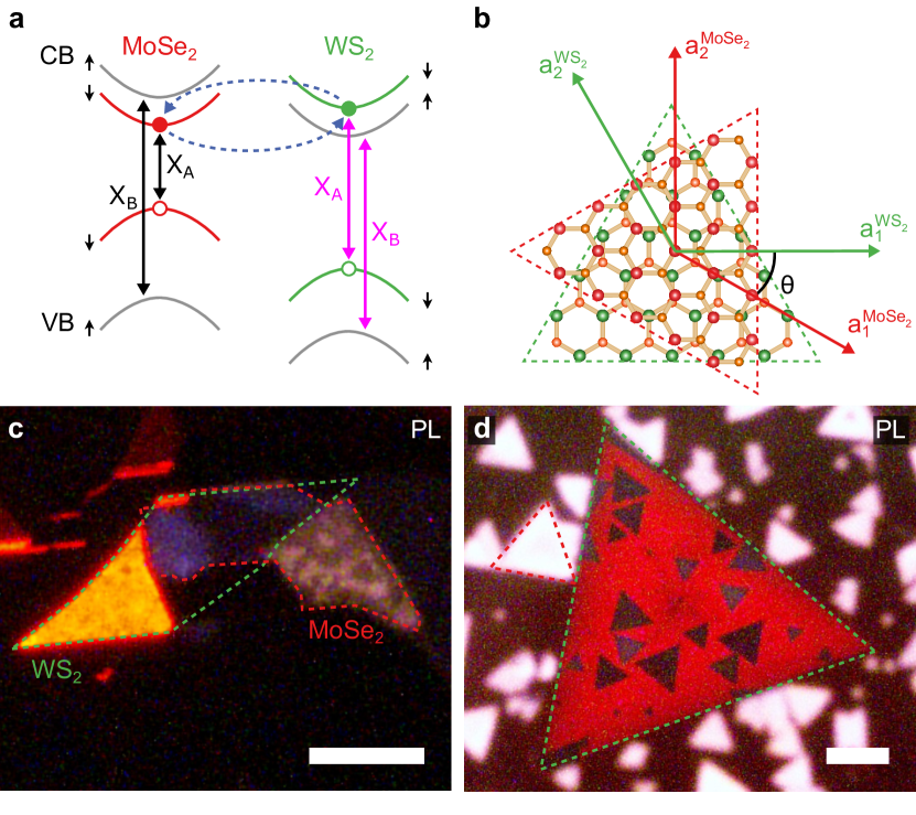
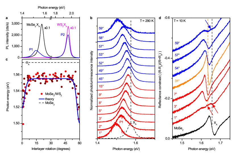
We have performed PL and RC studies over a wide range of temperatures on more than a 100 CVD and 5 mechanically exfoliated heterobilayers with various twist angles (defined in Fig. 1b). Figure 1 shows PL images Alexeev2017 of MoSe2/WS2 heterostructures assembled from mechanically exfoliated (c) and CVD-grown (d) monolayers. Fig. 2a compares room-temperature PL spectra of CVD-grown MoSe2 and WS2 monolayers, and a MoSe2/WS2 structure with . In the heterobilayer region, at energies close to the MoSe2 and WS2 intralayer A-exciton PL peaks (see Fig. 1a for the origin of the main optical transitions), P1 and P2 PL peaks are observed. P2 appears at the same energy as the monolayer WS2 PL line (), due to the strong signal collected from the surrounding monolayer WS2 (see Fig. 1d). By contrast, P1 displays a red shift with respect to the MoSe2 A exciton line at 1.573 eV.
Fig. 2b shows normalized PL spectra for the P1 peak for heterobilayers with twist angles approaching (red) and (blue). Strikingly, the P1 peak energy depends strongly on the twist angle, decreasing continuously as the stacking approaches lattice alignment (), or anti-alignment (). This is summarized in Fig. 2c, showing two distinct trends: a steep variation of for close to and , and a plateau at around 1.56 eV for large misalignment angles . The P1 integrated intensity and linewidth vary gradually as departs from ( Extended Data Figure 1a). The linewidth displays an additional sharp increase for twist angles close to and , similarly to the observed variation of the peak energy ( Extended Data Figure 1b).
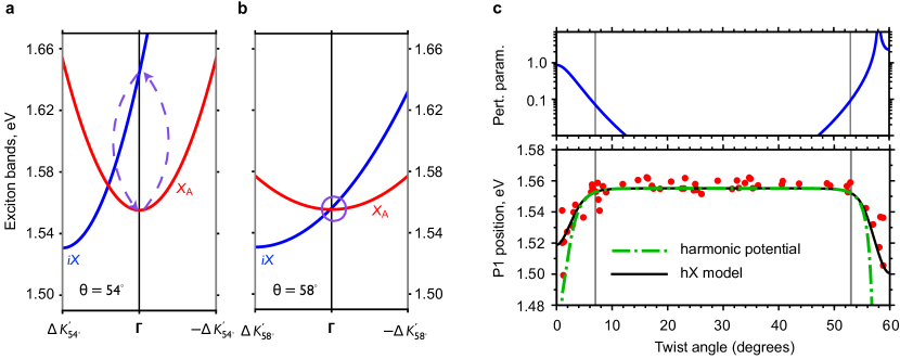
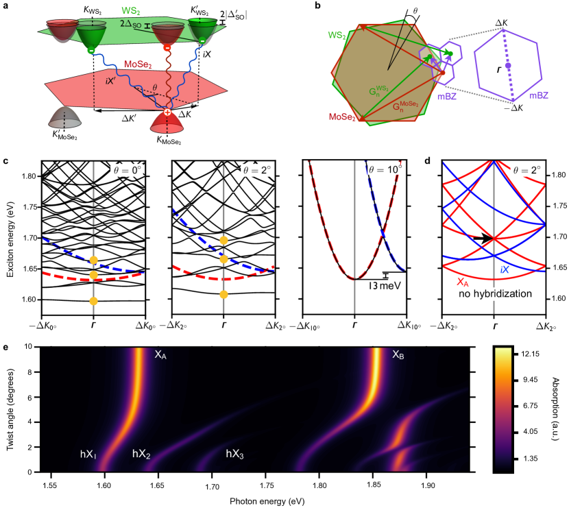
By contrast to the periodicity of the lattice and flake symmetry, the sharp variation of the P1 line energy and width with a period strongly suggests a connection to the misalignment between the monolayer Brillouin zones (BZs) produced by the twist, which introduces a momentum mismatch between the conduction and valence band edges of the two monolayers, located at their and valleys ( Fig. 3a-b) Zhang2017 . As shown in Fig. 3a, for perfect lattice alignment (anti-alignment), the valley mismatch () is minimized. In these configurations the MoSe2 A and B excitons are brought into close momentum-space proximity with interlayer excitons formed by MoSe2 holes and WS2 electrons, allowing them to hybridise through interlayer conduction-band tunnelling. Although the interlayer tunnelling strength has been estimated to be small for states at the BZ corners Wang2016b for TMD bilayers, the near resonance of the MoSe2 and WS2 conduction-band edges abinitio_1 ; abinitio_2 promotes hybridisation and the formation of hXs. This is similar to interlayer hybridization effects recently predicted Deilmann2018 ; Gerber2018 and experimentally observed Gerber2018 ; Slobodeniuk2018 in TMD homobilayers. We thus interpret the P1 line shift in Fig. 2 in terms of the twist-angle-dependent hX band structure. Furthermore, our theory reveals a strong influence of the moiré superlattice on the twist-angle dependent energies of bright hXs for twist angles near and (see Supplementary Notes 1 and 2 and Extended Data Figs. 2-4), which is beyond the scope of previous descriptions based on harmonic moiré potentials hongyi_moire ; mcdonald_intra .
The two lowest-energy bright interlayer excitons involving same-spin conduction and valence bands of opposite layers are shown in Fig. 3a, labeled iX and iX’, respectively. In general, at the bottom of their dispersions, iX and iX’ are expected to be “momentum-dark,” due to the rotational misalignment (Fig. 3a). However, for closely-aligned or anti-aligned structures, momentum-space proximity with the intralayer MoSe2 A exciton allows them to hybridise, given their shared hole band. The resulting hXs pick up oscillator strength from their XA component hX_theory , and their energies are sharply modulated for twist angles close to and . Analogously, MoSe2 B excitons (XB) can hybridise with iXs formed by carriers in the corresponding spin states. Note that spin-splitting and spin-valley locking of iXs lead to different energies and compositions of the hX states for and , producing the asymmetry seen in Fig. 2c.
The MoSe2 and WS2 conduction band states have plane-wave projections onto all Bragg vectors of their corresponding reciprocal lattices, and (red and green arrows in Fig. 3b). As a result, momentum conservation allows interlayer tunnelling between first BZ wave vectors of the two layers satisfying , where and are measured from the respective or valley, and are the first Bragg vectors of the moiré superlattice, which define the twist-angle-dependent mini Brillouin zone (mBZ) shown in purple in Fig. 3b (see also Extended Data Fig. 3).
The emergent periodicity leads to folding of the intra- and interlayer exciton bands into the mBZ, forming moiré mini bands, hybridised into hXs by interlayer electron tunnelling. Theoretically, this becomes evident in the twist-angle-dependent behaviour of the hX bands, which we calculate for along the momentum path (dotted line in Fig. 3b), with representing zero center-of-mass exciton momentum: as shown in Fig. 3c, a continuous energy drop of the lowest optically-active -hX as is observed. Experimentally, this behaviour is observed in PL as the P1 line red-shift of Figs. 2b,c, and a similar situation arises near , where the hX is formed by iX’ ( Extended Data Fig. 4). The calculated twist-angle dependence of the -hX energy is shown by the blue curve in Fig. 2c, obtained using a difference of between the XA and iX energies ( Fig. 3c), an electron hopping strength of , and setting the XA energy at room temperature to , as obtained from the plateau in the experimental data (Extended Data Table I). Furthermore, we attribute the sharp linewidth variation with twist angle for close to and , shown in Extended Data Fig. 1b, to the out-of-plane electric dipole moment of the hX state, inherited from its iX component, which makes the hX energy susceptible to random electric fields (see Supplementary Note 3).
Figure 3e shows calculated absorption spectra for the heterobilayer as a function of twist angle, predicting three-peak structures close to the XA and XB energies for twist angles close to . In this case, we have used an XA energy of , corresponding to our exfoliated samples (see below), and kept the same X-iX detuning and hopping strength obtained from the CVD data ( see Extended Data Table I). The peaks labeled hX1 and hX2 are two hX states resulting from resonant hybridisation of the XA band with the lowest-energy iX band at the point. The energy shift of hX1 with twist angle indicates that it corresponds to P1 in our PL measurements, whereas the transfer of the oscillator strength from hX1 to hX2 for shows enhanced mixing of the former with the -iX state. By contrast, the hX3 peak originates from the first moiré mini band, formed by folding of the XA band onto the mBZ. This is illustrated in Fig. 3e, where we have set the XA-iX tunnelling strength to zero, such that the red (blue) bands represent pure XA (iX) states. The black arrow indicates the point where the first XA moiré mini bands cross the point. For non-zero tunnelling, these mini bands will mix with the bright -XA state below. In other words, hX3 becomes semi-bright through moiré umklapp processes that mediate the exciton-photon interaction hX_theory , and constitutes a direct signature of the moiré effects on the exciton band structure. An analogous three-line structure appears in the calculated spectrum near XB, around eV in Fig. 3d.
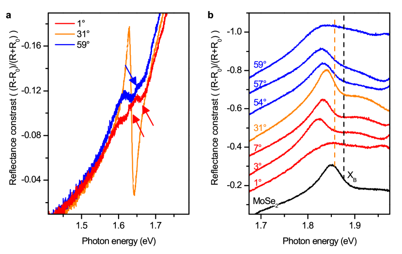
We carried out RC measurements of the same CVD-grown heterostructures at low temperature, where the spectral linewidths are narrower. Fig. 2d shows the RC spectra measured at =10K for several CVD MoSe2/WS2 heterobilayers and a MoSe2 monolayer. Similarly to room-temperature PL, we observe in Fig. 2d a 20 meV red-shift of the XA exciton resonance in the misaligned heterobilayer (orange) for =31∘, as compared to the uncoupled monolayer (black). The strong red-shift of the RC peaks and significant reduction of their intensities observed for close to and is consistent with our room-temperature PL measurements. In addition, note the appearance of weak new features in the spectra for and , within 50 meV above the main reflectance feature ( Fig. 2d and Extended Data Fig. 5a). We associate these spectral signatures with the absorption peaks hX1,2,3 in Fig. 3d. Similar twist-angle-dependent red-shifts are also observed in the vicinity of the XB energy, as shown in Extended Data Fig. 5b, where also a clear reduction of the intensity of the RC peaks is evident for approaching and , consistent with Fig. 3d. However, no additional features are distinguishable, due to the broader XB linewidth.
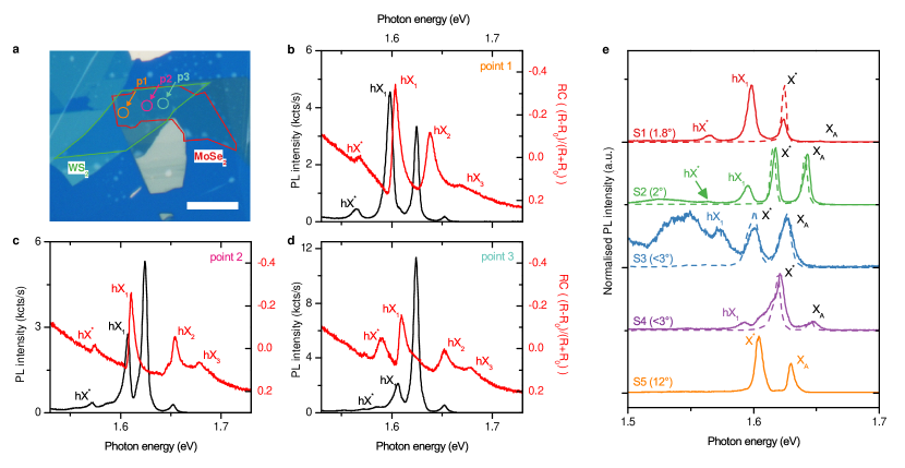
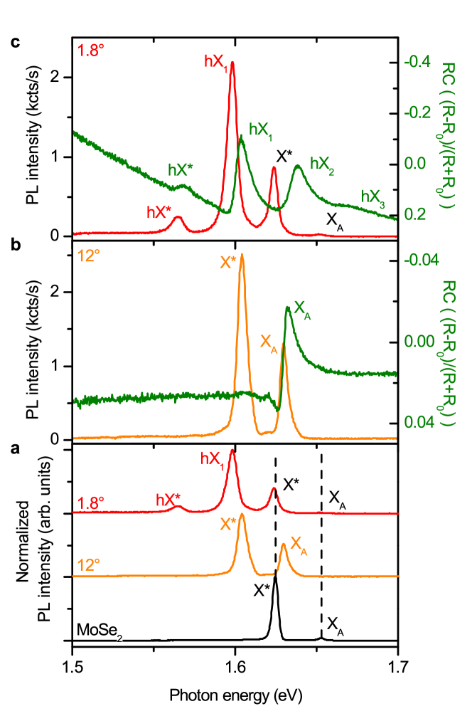
A dramatic improvement in both RC and PL spectral resolution is observed in the high-quality MoSe2/WS2 heterostructures, assembled in a glove-box from mechanically exfoliated monolayers and fully encapsulated in hBN. Figure 4a shows a comparison of normalised PL spectra measured for a monolayer MoSe2 (black), and MoSe2/WS2 heterobilayers with of 12∘ (orange) and (red). The black and red spectra are measured in a single sample, where in addition to the heterobilayer, a monolayer MoSe2 region is also present. The PL spectrum for the monolayer area shows a very pronounced trion (charged exciton) peak, labeled X* (with intensity exceeding 120000 counts/s/), and a weaker neutral exciton, XA. In the structure with misaligned MoSe2 and WS2 monolayers, both peaks red-shift by around 20 meV (orange spectrum). In this sample, MoSe2 completely overlaps with WS2, and thus no PL from uncoupled MoSe2 is observed. For the high-quality aligned heterobilayer (, red spectrum), the PL spectrum shows 4 peaks with a maximum intensity of 1500 counts/s/. As can be deduced from the identical spectral positions, the two peaks at higher energies correspond to PL collected from the remote MoSe2 monolayer area. The other two features, labeled hX* and hX1, originate in the heterostructure region and exhibit a strong red shift of 38 and 32 meV from X* and XA in the structure, respectively, consistent with the behaviour observed in the CVD samples. We observed similar PL spectra in other high-quality exfoliated samples (Extended Data Fig. 6e).
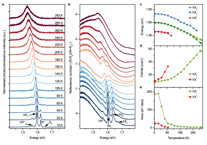
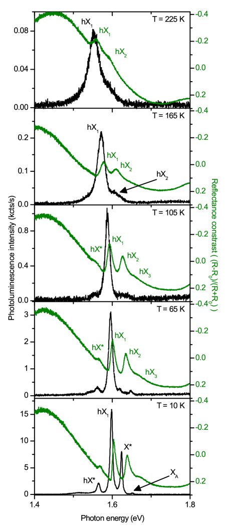
The green curve in Fig. 4b shows the RC spectrum of the exfoliated heterobilayer with , where a single strong resonance corresponding to the XA transition is observed. In stark contrast, four features are clearly observed in the RC spectrum of the aligned sample ( Fig. 4c and Extended Data Fig. 6b-d), labeled as hX*, hX1, hX2 and hX3. hX* and hX1 directly correspond to the identically labeled peaks in PL, whereas the new features hX2 and hX3 are unrelated to X* and XA peaks observed in the monolayer MoSe2 PL spectrum. We attribute hX2 and hX3 to the moiré miniband states of hybridised excitons labeled in Fig. 3d. Temperature dependent studies in Fig. 5 show that all hX peaks persist in RC spectra up to 105 K, above which the observation of hX* and hX3 becomes difficult due to broadening. We tentatively ascribe hX* to a recombination of hybridised excitons bound to an additional charge. At room temperature (Extended Fig. 7), the most pronounced peak in PL and RC is hX1, supporting its identification with PL peak P1 in Fig. 2. Cooling down to K is necessary for unambiguous identification of hX2, as shown in Fig. 5. On the other hand, while the PL trion peak X* vanishes at K, a new PL feature corresponding to hX2 appears for K due to thermal activation, in agreement with our calculations (see Supplementary Note 1 and Extended Data Fig. 8).
Moiré excitons have been previously discussed hongyi_moire ; mcdonald_intra ; MacDonald_moireX ; Xu_moireX in type-II TMD heterobilayers with strong detuning between the band edges of their constituting layers Zhang2018 . In those cases, interlayer hybridisation of carriers is weak, and the moiré effects are dominated by a periodic exciton potential produced by the band gap modulation along the heterostructure plane. Our results indicate that resonant interlayer hybridisation in MoSe2/WS2, such as studied here, is the dominant mechanism driving moiré superlattice effects, producing hX states that inherit spectral properties of the intralayer and interlayer excitons. Our PL and RC measurements for varying twist angle in both CVD and exfoliated samples provide strong evidence for the appearance of semi-bright hybridised exciton states, and in particular for spectral features originating from higher hybridised moiré exciton mini bands, enabled by umklapp exciton-photon processes mediated by the moiré superlattice. We anticipate a similar effect of the hybridised exciton formation and resonant enhancement of moiré superlattice effects in a broader class of 2D material heterostructures with close conduction or valence band alignment. In such materials, the twist-angle-controlled resonant effects reported in this work constitute an unprecedented approach for carrier and exciton band structure engineering.
I References
References
- (1) Geim, A. K. & Grigorieva, I. V. Van der Waals heterostructures. Nature 499, 419 (2013).
- (2) Novoselov, K. S., Mishchenko, A., Carvalho, A. & Castro Neto, A. H. 2D materials and van der Waals heterostructures. Science 353 (2016).
- (3) Kuwabara, M., Clarke, D. R. & Smith, D. A. Anomalous superperiodicity in scanning tunneling microscope images of graphite. Applied Physics Letters 56, 2396–2398 (1990).
- (4) Yankowitz, M. et al. Emergence of superlattice Dirac points in graphene on hexagonal boron nitride. Nature physics 8, 382–386 (2012).
- (5) Dean, C. R. et al. Hofstadter’s butterfly and the fractal quantum Hall effect in moiré superlattices. Nature 497, 598–602 (2013).
- (6) Hunt, B. et al. Massive dirac fermions and hofstadter butterfly in a van der Waals heterostructure. Science 340, 1427–1430 (2013).
- (7) Mishchenko, A. et al. Twist-controlled resonant tunnelling in graphene/boron nitride/graphene heterostructures. Nature nanotechnology 9, 808–13 (2014).
- (8) Cao, Y. et al. Unconventional superconductivity in magic-angle graphene superlattices. Nature 556, 43–50 (2018).
- (9) Withers, F. et al. Light-emitting diodes by band-structure engineering in van der Waals heterostructures. Nature materials 14, 301–306 (2015).
- (10) Rivera, P. et al. Interlayer valley excitons in heterobilayers of transition metal dichalcogenides. Nature Nanotechnology 13, 1004–1015 (2018).
- (11) Mak, K. F. & Shan, J. Photonics and optoelectronics of 2D semiconductor transition metal dichalcogenides. Nature Photonics 10, 216–226 (2016).
- (12) Yu, H., Liu, G.-B. B., Tang, J., Xu, X. & Yao, W. Moiré excitons: From programmable quantum emitter arrays to spin-orbit coupled artificial lattices. Science Advances 3, e1701696 (2017).
- (13) Wu, F., Lovorn, T. & Macdonald, A. H. Topological exciton bands in Moiré heterojunctions. Physical Review Letters 118 (2017).
- (14) Heo, H. et al. Interlayer orientation-dependent light absorption and emission in monolayer semiconductor stacks. Nature Communications 6, 7372 (2015).
- (15) Nayak, P. K. et al. Probing evolution of twist-angle-dependent interlayer excitons in MoSe2/WSe2 van der Waals heterostructures. ACS Nano 11, 4041–4050 (2017).
- (16) Kunstmann, J. et al. Momentum-space indirect interlayer excitons in transition-metal dichalcogenide van der Waals heterostructures. Nat. Phys. (2018).
- (17) Liu, K. et al. Evolution of interlayer coupling in twisted molybdenum disulfide bilayers. Nature Communications 5, 4966 (2014).
- (18) Van Der Zande, A. M. et al. Tailoring the electronic structure in bilayer molybdenum disulfide via interlayer twist. Nano Letters 14, 3869–3875 (2014).
- (19) Tran, K. et al. Moiré excitons in van der Waals heterostructures. arXiv 1807.03771 (2018).
- (20) Seyler, K. L. et al. Signatures of moiré-trapped valley excitons in MoSe2/WSe2 heterobilayers. arXiv 1809.04562 (2018).
- (21) Kozawa, D. et al. Evidence for interlayer energy transfer in MoSe2/WS2 heterostructures. Nano Letters 16, 4087–4093 (2016).
- (22) Alexeev, E. M. et al. Imaging of interlayer coupling in van der Waals heterostructures using a bright-field optical microscope. Nano Letters 17, 5342–5349 (2017).
- (23) Zhang, C. et al. Interlayer couplings, moire patterns, and 2D electronic superlattices in MoS2/WSe2 hetero-bilayers. Science Advances 3, e1601459 (2017).
- (24) Wang, Y., Wang, Z., Yao, W., Liu, G. B. & Yu, H. Interlayer coupling in commensurate and incommensurate bilayer structures of transition-metal dichalcogenides. Physical Review B 95, 39–41 (2017).
- (25) Kang, J., Tongay, S., Zhou, J., Li, J. & Wu, J. Band offsets and heterostructures of two-dimensional semiconductors. Applied Physics Letters 102, 012111 (2013).
- (26) Gong, C. et al. Band alignment of two-dimensional transition metal dichalcogenides: Application in tunnel field effect transistors. Applied Physics Letters 103, 053513 (2013).
- (27) Deilmann, T. & Thygesen, K. S. Interlayer excitons with large optical amplitudes in layered van der Waals materials. Nano Letters 18, 2984–2989 (2018).
- (28) Gerber, I. C. et al. Interlayer excitons in bilayer MoS2 with strong oscillator strength up to room temperature. arXiv 1811.06469 (2018).
- (29) Slobodeniuk, A. O. et al. Fine structure of k-excitons in multilayers of transition metal dichalcogenides. arXiv 1810.00623 (2018).
- (30) Ruiz-Tijerina, D. A. & Fal’ko, V. I. Resonantly enhanced moiré superlattice coupling in heterostructures and transition-metal dichalcogenide bilayers with matching band edges. arXiv 1809.09257 (2018).
- (31) Zhang, N. et al. Moiré intralayer excitons in a MoSe2/MoS2 heterostructure. Nano Letters 18, 7651 7657 (2018).
- (32) Kormányos, A. et al. k · p theory for two-dimensional transition metal dichalcogenide semiconductors. 2D Materials 2, 022001 (2015).
- (33) Danovich, M. et al. Localized interlayer complexes in heterobilayer transition metal dichalcogenides. Phys. Rev. B 97, 195452 (2018).
II Acknowledgments
The authors thank the financial support of the European Graphene Flagship Project under grant agreement 696656, EC Project 2D-SIPC, and EPSRC grant EP/P026850/1. E.M.A. and A.I.T. acknowledge support from EPSRC grants EP/M012727/1 and the European Union’s Horizon 2020 research and innovation programme under ITN Spin-NANO Marie Sklodowska-Curie grant agreement no. 676108. D.A.R-T. and V.I.F. acknowledge support from ERC Synergy Grant Hetero2D, EPSRC EP/N010345, and the Lloyd Register Foundation Nanotechnology grant. K.S.N. thanks financial support from the Royal Society, EPSRC, US Army Research Office and ERC Grant Hetero2D. H.S.S. acknowledge the research fund (NRF-2017R1E1A1A01074493) by National Research Foundation by the ministry of Science and ICT, Korea. M.R.M. acknowledges support from the National Science Centre (no. UMO-2017/24/C/ST3/00119). R.V.G. acknowledges financial support from the Royal Society Fellowship Scheme and EPSRC CDT Graphene-NOWNANO EP/L01548X. K.W. and T.T. acknowledge support from the Elemental Strategy Initiative conducted by the MEXT, Japan and the CREST (JPMJCR15F3), JST.
III Author contributions
E.M.A. carried out microscopy and optical spectroscopy experiments. E.M.A. and A.I.T. analyzed optical spectroscopy data. D.A.R.-T., M.D., V.I.F. developed the theory. P.K.N., S.A., S.P, J.L., J.I.S. and H.S.S. carried out CVD growth of the monolayers and fabricated the heterobilayer samples. M.J.H., D.J.T. and R.G. fabricated mechanically exfoliated samples using glove box techniques. M.R.M. and M.K. carried out SHG measurements on exfoliated samples. K. W. and T. T. synthesized the hBN crystals. E.M.A., D. A.R.-T., A.I.T. and V.I.F. wrote the manuscript. E.M.A., K.N.S., V.I.F. and A. I. T. conceived the experiment. All authors participated in discussions. A. I. T. oversaw the project.
IV Author Information
Correspondence and requests for materials should be addressed to Alexander Tartakovskii at a.tartakovskii@sheffield.ac.uk and Vladimir Fal’ko at Vladimir.Falko@manchester.ac.uk.
V Figure captions
Figure 1. Twisted MoSe2/WS2 heterobilayers.
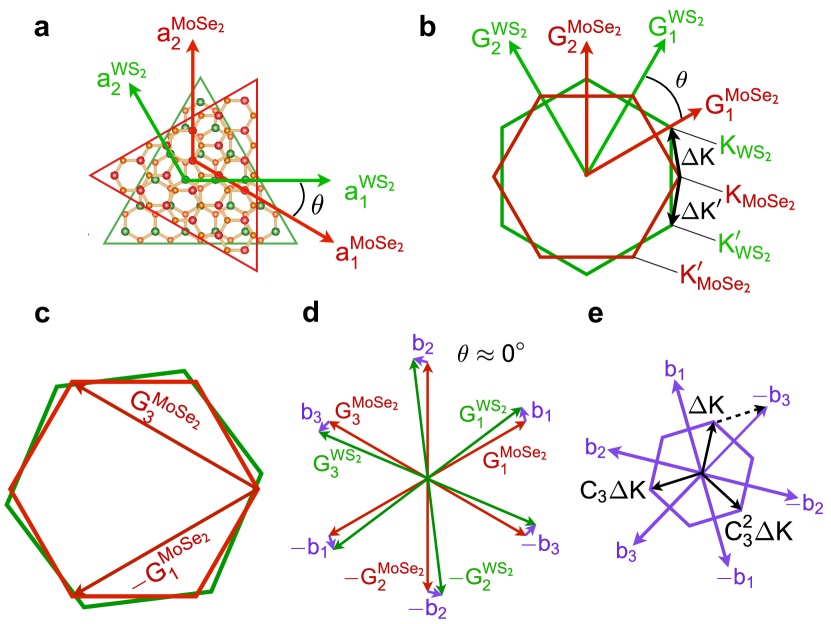
(a) Schematic band diagram of MoSe2/WS2 showing staggered alignment of the valence bands (VB) and the near degeneracy of the conduction band (CB) edges. The carrier spin orientations are labeled, and the spin-orbit splittings are schematically shown as energetically separated valence and conduction sub-bands. CB and VB states involved in the formation of the bright A and B excitons to are connected by arrows. The dashed arrows represent resonant hybridisation between conduction band states of the two layers. (b) Real–space configuration of the heterobilayer. Mo (W) atoms are shown in red (green), and all chalcogens are depicted in orange. The angle between same lattice vectors of the two layers, e.g. and , translates into an angle between the reciprocal lattice vectors, resulting in misalignment of the two Brillouin zones.
(c) PL image of one of the studied mechanically exfoliated hBN/MoSe2/WS2/hBN samples acquired using a modified optical microscope (see Methods and Ref. Alexeev2017 for details). Orange and pink correspond to PL emitted from WS2 and MoSe2 regions, respectively. Edges of the monolayer flakes are marked. Dark (low PL) areas correspond to the heterobilayer region where the WS2 and MoSe2 intralayer A exciton PL is quenched. (d) PL image of one of the studied heterobilayers assembled from CVD-grown monolayers, where red and pink correspond to PL from WS2 and MoSe2, respectively. The scale bar in (c) and (d) corresponds to 10 m.
Figure 2. Optical properties of twisted MoSe2/WS2 heterobilayers. (a) Room-temperature PL spectra measured in CVD-grown MoSe2 (black) and WS2 (magenta) monolayers, as well as in a mechanically stacked MoSe2/WS2 heterostructure with rotation angle between the layers (blue). The two PL peaks appearing in the heterobilayer are labeled P1 and P2. (b) Normalized PL spectra showing peak P1 from (a) acquired in MoSe2/WS2 heterobilayers with interlayer twist angles ranging from 1 to 59∘, indicated above each curve. A typical PL spectrum for a monolayer MoSe2 is shown with a dashed black curve. The MoSe2 A exciton PL peak is labeled XA, and its energy is marked with the vertical dashed line. (c) Variation of the P1 PL peak energy with twist angle measured on two substrates containing MoSe2/WS2 heterobilayers. Data for individual substrates are shown with light and dark red symbols. See description of the fitting procedure in Methods. The blue curve shows results of theoretical calculations as described in the text and Supplementary Note 1. The dashed horizontal line shows the spectral position of XA in an isolated MoSe2 monolayer. (d) Low temperature (T=10 K) reflectance contrast (RC) spectra measured near the A exciton energy in an isolated MoSe2 monolayer (black), and in MoSe2/WS2 heterostructures with various twist angles (with values shown next to each curves). See explanation of the RC experiment, in particular parameters and , in Methods. The A exciton feature in the isolated MoSe2 monolayer spectrum is labeled XA. Arrows indicate new RC features appearing in the spectra for structures with nearly perfect (anti-)alignment. Vertical lines show the positions of the maximum derivative of the XA feature in the monolayer (black) and misaligned heterobilayer (orange) spectra.
Figure 3. Theoretical moiré bands and absorption spectrum of hybridised excitons. (a) MoSe2 and WS2 electronic band structures and BZ alignment for twist angle (the conduction band spin-orbit couplings and are exaggerated for clarity). Spin-down (spin-up) bands are coloured red or green (grey). The wavy red line represents the formation of the zero-momentum MoSe2 A exciton, XA. The two interlayer exciton states iX and iX’, involving WS2 electrons of opposite valleys, are shown with wavy blue lines. (b) Moiré mini Brillouin zone (mBZ, purple) defined by the moiré Bragg vectors (purple arrows).
(c) hybridised exciton (hX) bands along the mBZ path defined in (b) for twist angles and (for angles close to , see Extended Data Fig. 4). For reference, the decoupled intra- and interlayer (iX) exciton bands are shown in red and blue dashed curves, respectively. Optically active hybridised exciton states in that energy range are marked with yellow dots, whereas unmarked excitons are of iX nature. (d) Absorption spectrum as a function of twist angle. The MoSe2 A and B exciton resonances XA and XB are indicated for large twist angles, where hybridisation effects become negligible. By contrast, the three lines labeled hX1,2,3 appearing for correspond to bright resonantly hybridised excitons in the range of MoSe2 XA; analogous features in the range of XB are not labeled. In particular, hX3 originates from hybridisation of the first folding of the XA band into the mBZ with the bright zero-momentum XA state, indirectly through the iX band. This is illustrated in (e), where we show the XA (red) and iX (blue) bands in the absence of hybridisation, for clarity. The black arrow indicates the point where the first folded XA bands cross the point. Thus, hX3 constitutes a direct signature of the moiré superlattice effect.
Figure 4. Low temperature (T=10 K) optical spectra for exfoliated MoSe2/WS2 heterobilayers and MoSe2 monolayers. (a) PL spectra of the MoSe2 monolayer (black), misaligned MoSe2/WS2 heterobilayer with (orange), and the aligned MoSe2/WS2 heterobilayer with (red). All samples are encapsulated in hBN. Black and red spectra are measured in the same sample, where an uncoupled MoSe2 monolayer was present. Vertical lines mark the positions of A exciton (XA) and trion (X*) resonances in the uncoupled MoSe2 monolayer, also visible in the red spectrum due to the monolayer proximity and its much stronger PL (see text and Extended Data Fig. 6). Peak hX1 appears in the PL spectrum of the sample, as predicted in Fig. 3d, together with an additional interlayer exciton line hX∗ (see text). (b) PL (orange) and RC (green) spectra for the misaligned MoSe2/WS2 heterobilayer, with . XA labels the A exciton RC and PL features. (c) PL (red) and RC (green) spectra for the aligned MoSe2/WS2 heterobilayer, with . In addition to hX1 and hX∗, two other features, hX2 and hX3, appear in the RC spectrum, in agreement with Fig. 3d.
Figure 5. Temperature-dependent PL and RC spectra for aligned MoSe2/WS2 heterobilayer. The data are shown for the same sample with hBN-encapsulated MoSe2/WS2 heterobilayer with , for which the low temperature data are presented in Fig. 4c. Here, PL and RC spectra are shown in black and green, respectively. Similarly to Fig. 4c, RC and PL peaks are labeled hX* and hX1-3. X* and XA mark PL peaks from the remote isolated MoSe2 monolayer. The bottom panel presents the same low temperature data as shown in Fig.4c.
VI Methods
Fabrication of twisted MoSe2-WS2 heterobilayers
Triangle-shaped monolayers of MoSe2 and WS2 were produced by chemical vapor deposition (CVD) growth. Single–layer MoSe2 crystals were grown on a c-plane sapphire substrate by the vaporization of MoO3 and Se powders in a 2-inch quartz tube furnace in a controlled gaseous environment. A typical run consisted of loading 60 mg of MoO3 source powder and 100 mg of Se powder into two ceramic boats, which were then placed into the center heating zone and upwind the low temperature zone in the same quartz tube. A piece of sapphire substrate, acting as a deposition acceptor, was placed downstream adjacent to the MoO3 powder. The temperature of MoO3 powder was raised to 600∘ C at a rate of 25∘C/min and then increased to 700∘ C within 10 min. At the same time, the temperature of the Se powder was raised to 275∘ C using an external heating coil. After reaching their target values, the temperatures of MoO3 and Se were maintained at the same levels to facilitate the MoSe2 growth. The vapor-phase reactants were transported by Ar gas flow (60 sccm), and selenization was carried out by the flowing H2 reductant gas (12 sccm), thereby facilitating the growth of the 2D MoSe2 crystals at the growth region. At the end of the growth, the furnace was fast cooled to room temperature in a pure Ar atmosphere.
For WS2 growth, 50 mg of WO3 powder were placed at the center of an alumina boat, and a silicon substrate with a 300 nm-thick SiO2 layer was placed upside down above it. Another alumina boat containing 200 mg of sulfur powder was placed upstream of the furnace. The furnace was heated to 950∘C and the temperature was maintained for 20 minutes with a flow of Ar gas (150 sccm) in order to grow monolayer WS2. The furnace was then allowed to cool down naturally.
For twisted heterobilayer fabrication, the monolayer MoSe2 flakes grown on a sapphire substrate were transferred onto a 300 nm SiO2/Si substrate using a poly(methyl methacrylate) (PMMA) transfer process. Few drops of PMMA (950 K) were spin-coated on the MoSe2/sapphire substrate at 4000 RPM for 60 second and backed at 120∘ C for 30 min. To facilitate the separation of the PMMA membrane, a drop of deionized water was put at the interface between PMMA and sapphire substrate. The PMMA-coated MoSe2 monolayers were then peeled off the substrate using sharp tweezers and transferred into deionized water. The floating PMMA/MoSe2 membrane was transferred onto a prepared WS2/(SiO2/Si) substrate and dried at 80∘ C for few minute to evaporate the water at the interface. Finally, the PMMA layer was dissolved in acetone, and the substrate was cleaned using isopropyl alcohol.
High-quality fully-encapsulated MoSe2/WS2 samples were fabricated using PMMA-assisted dry-peel transfer. In order to minimize contamination, heterostructures were fabricated using remotely controlled micro-manipulation setup placed inside an argon chamber with 0.1 ppm O2 and H2O. The bulk MoSe2 and WS2 crystals were mechanically exfoliated onto a 90 nm layer of PMMA coated on a silicon wafer. Monolayers were then identified via optical microscopy, as well as through luminescence imaging in the dark-field configuration for WS2 Alexeev2017 . Those crystals which had adjacent straight edges at 0∘, 60∘ or 120∘ to one another (indicating one of the crystallographic axes) were then selected and picked up onto an hBN film ( 10 nm thickness) held by a PMMA membrane. During the transfer of the second TMD layer the edges were aligned to within 2∘ of the desired angle and finally transferred onto another hBN film ( 20 nm) exfoliated onto an oxidised silicon wafer (70 nm SiO2) to achieve full encapsulation. In order to prevent spontaneous rotation of the TMDC layers and deterioration of MoSe2 crystalline quality we avoided exposing the heterostructures to the temperatures above 70∘ C.
Twist angle measurements and spectral fitting.
The interlayer twist angle in CVD MoSe2/WS2 heterobilayers was extracted from the microscope images by comparing the orientation of the two materials. It has been shown [35,36] that triangular transition-metal dichalcogenide (TMD) flakes have zigzag edges, which appear sharp or diffuse in microscopy images when the edges terminate with transition metal atoms or chalcogens, respectively. Therefore, as the sharp terminations of the flakes shown in Fig. 1d of the main text indicate transition-metal termination, the relative flake orientation directly corresponds to the twist angles between their lattice vectors, up to rotations given the rotational symmetry of both the flakes and their underlying lattices. Similarly, for flakes with the boundaries of different types, the interlayer twist angle is determined by subtracting 60∘ from the relative rotation measured from the microscope image.
With these considerations, we were able to determine the relative twist angles between the different MoSe2 flakes and the bottom WS2 monolayer from the microscopy images with accuracy. Inherent to our method is an uncertainty in the angular measurement when the type of the flake boundary is not clear, and the edge may be formed by either transition metal or chalcogen atoms.
Although only a few of our samples displayed these characteristics, this uncertainty may be behind the symmetric shape of the data presented in Fig. 2c and Extended Data Fig. 1b.
To identify the relative twist angle of the exfoliated TMD monolayers, second harmonic generation (SHG) measurements were performed [37], see Extended Data Fig.9. All SHG measurements were taken at room temperature using a custom-built system with a Toptica FemtoFErb fs SAM mode-locked laser with a repetition rate of 80 MHz centred at 785 nm. For each measurement, the laser light had a typical incident power of 500 W, was linearly polarized and focused to a spot size of 2 m by a 50x objective lens (NA = 0.36). The SHG signal was separated from the reflected light using of a beam splitter and short-pass filter. A second linear polarizer (analyzer) was placed in the SHG signal path and aligned parallel to the excitation polarization. A motorized half-wave plate was located above the objective and rotated in order to obtain angle resolution. The SHG signal for each measurement was then processed by a spectrometer with a grating of 300 groves per millimetre and exposed onto a liquid nitrogen cooled charge-coupled device for 5 seconds.
The position, width and integrated intensity of the hybridized exciton peak were extracted from the room-temperature PL spectra of the corresponding regions by fitting with a single Lorentzian peak. In several regions, however, the proximity to isolated monolayer areas or the presence of contamination trapped between the layers has led to the detection of an uncoupled MoSe2 signal, which appears as a high-energy shoulder in the PL spectrum (see top curve in Fig. 2b). The PL spectra containing isolated MoSe2 signal were fitted with two Lorentzian peaks, and the parameters of the lower-energy peak were used for the twist angle dependence.
Photoluminescence imaging, and photoluminescence and reflectance contrast spectroscopy.
The photoluminescence (PL) images of the heterobilayer samples were acquired using a modified bright-field microscope (LV150N, Nikon) equipped with a color camera (DS-Vi1, Nikon). The near-infrared emission from the white light source was blocked with a 550 nm short-pass filter (FESH0550, Thorlabs), and a 600 nm long-pass filter (FELH0600, Thorlabs) was used to isolate the PL signal from the sample. The full description of the system is available in Ref. Alexeev2017, .
Spectrally–resolved PL and reflectance contrast (RC) measurements were performed using a custom-built micro-PL setup. For PL, the excitation light centred at 2.33 eV was generated by a diode-pumped solid-state laser (CW532-050, Roithner), while for RC a stabilized Tungsten-Halogen white-light source (SLS201L, Thorlabs) was used. The excitation light was focused onto the sample using a 50x objective lens (M Plan Apo 50X, Mitutoyo). The PL and RC signals collected in the backwards direction were detected by a 0.5 m spectrometer (SP-2-500i, Princeton Instruments) with a nitrogen cooled CCD camera (PyLoN:100BR, Princeton Instruments). The PL signal was isolated using a 550 nm short-pass filter (FELH0550, Thorlabs). The RC spectra were derived by comparing the spectra of white light reflected from the sample and the substrate as , where () is the intensity of light reflected by the sample (substrate). The room-temperature measurements were performed in ambient conditions. The low temperature measurements were carried out using a continuous flow liquid helium cryostat, where the sample was placed on a cold finger with the base temperature of 10 K.
References for Methods
[35] van der Zande, A. M. et al. Grains and grain boundaries in highly crystalline monolayer molybdenum disulphide. Nature Materials 12, 554-561 (2013).
[36] Zhu, D. et al. Capture the growth kinetics of CVD growth of two-dimensional MoS2. npj 2D Materials and Applications 1, 8 (2017).
[37] Hsu, W.-T. et al. Second harmonic generation from artificially stacked transition metal dichalcogenide twisted bilayers. ACS Nano 8, 2951-2958 (2014).
VII Figures
VIII Extended Data Figure Captions and Extended Data Table
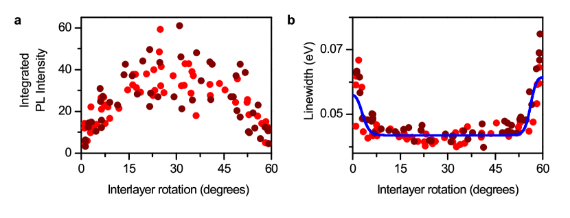
Extended Data Figure 1. Integrated intensity and linewidth for room-temperature PL spectra for MoSe2/WS2 heterobilayers as a function of the interlayer twist angle . (a) and (b) shows the variation of integrated intensity and linewidth, respectively. See Methods for the description of the fitting procedure. Data acquired on two individual substrates containing MoSe2/WS2 heterobilayers made from CVD-grown monolayers of MoSe2 and WS2 are shown with light and dark red symbols. The blue curve shows results of theoretical calculations as described in Supplementary Note 3.
Extended Data Figure 2. Breakdown of the moiré harmonic potential approximation in MoSe2/WS2. (a) MoSe2 A-exciton (XA, red) and interlayer exciton (iX, blue) bands in MoSe2/WS2 within the moiré Brillouin zone, for twist angle . Purple arrows represent second-order virtual tunnelling process enabled by intralayer-interlayer exciton hybridization, giving rise to a moiré potential for bright (-point) MoSe2 A excitons. (b) Perturbation theory breaks down for MoSe2 -point A excitons at , due to the exciton band crossing. As a result, the effective moiré potential diverges for this twist angle, indicating that the harmonic potential approximation is invalid. (c) Perturbative parameter (top, see Supplementary Note 2) and P1 PL line energy (bottom). The vertical gray lines divide the plot into the plateau and the two modulation regions, showing that the latter is always outside the region of validity of the harmonic approximation.
Extended Data Figure 3. The moiré mini Brillouin zone in MoSe2/WS2 heterobilayers. (a) Real-space stacking of the MoSe2 (red) and WS2 (green) lattices for twist angle , with lattice vectors labeled . Red (green) circles represent Mo (W) atoms, whereas Se and S atoms are shown as orange circles. (b) The resulting alignment between the Brillouin zones. Corresponding reciprocal lattice vectors and appear misaligned by the twist angle . The monolayer band edges appear at the points of the corresponding BZs; the valley mismatch vectors are labeled and . (c) The two MoSe2 Bragg vectors that contribute to the hopping term in Eq. 3 in Supplementary Note 1. (d) First circle of Bragg vectors for the two TMD crystals, defining the moiré vectors for . (e) Mini Brillouin zone defined by the vectors , where the lattice mismatch appears at the mBZ edge. The different moiré vectors can be constructed as . An example is shown, where .
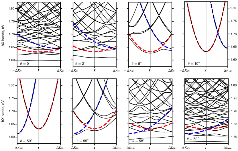
Extended Data Figure 4. Calculated moiré band structures of hybridized excitons in MoSe2/WS2 heterobilayers for various interlayer twist angles. Bright hybridized exciton (hX) band structures within the first moiré Brillouin zone for various twist angles, calculated using the exfoliated sample parameters reported in Extended Data Table I. The red dashed curves in all panels show the uncoupled MoSe2 A exciton dispersion, for reference. In the top panels, the blue dashed curves corresponds to the iX interlayer exciton state described in the main text, whereas in the bottom panels they represent the interlayer exciton state labeled iX’.
Extended Data Figure 5. Low-temperature RC spectra of CVD-grown MoSe2/WS2 heterobilayers. (a) RC spectra recorded at T = 10 K in CVD MoSe2/WS2 heterostructure with interlayer twist angle of 1∘ (red), 31∘ (orange) and 59∘ (blue) in a spectral range around the MoSe2 A exciton energy. Closely-aligned regions show the red shift and significant intensity reduction of the main peak compared to the rotationally misaligned heterobilayer, as well as the emergence of additional weak features above the main peak. (b) RC spectra measured in the vicinity of the B exciton energy in an isolated MoSe2 monolayer (black), and in MoSe2/WS2 heterostructures for various . The B exciton feature in the isolated MoSe2 monolayer spectrum is labeled XB. Vertical lines show the position of the maximum derivative of the XB feature in the monolayer (black) and misaligned heterobilayer (orange) spectra. See full description of the experimental procedure for the RC measurements in Methods.
Extended Data Figure 6. Variation of PL and RC spectra in a MoSe2/WS2 heterobilayers made from exfoliated MoSe2 and WS2 monolayers encapsulated in hBN. (a) Bright-field image of a fully-encapsulated MoSe2/WS2 sample S1, where the points for which we report the PL and RC spectra in (b)-(d) are marked. Scale bar corresponds to 10 m.(b-d) Low-temperature PL (black) and RC (red) spectra recorded in several regions of the sample marked in (a). The two higher-energy peaks in the PL spectra, X* at 1.624 and XA at 1.652 eV, correspond to trion and excition emission unintentionally collected from the single-layer MoSe2 area located at the right side of the heterobilayer sample. The position of these peaks remains unchanged in all three points, while their intensity decreases gradually with the increasing spatial separation. The two lower-energy PL peaks, labeled hX∗ and hX1, represent the emission originating in the heterostructure region and show a variation of their position and relative intensities across the heterostructure region, likely caused by the non-uniform strain and doping. The RC spectra recorded in the three points are similar, with the two lower-energy peaks directly corresponding to hX∗ and hX1 in PL, and hX2 and hX3 representing the higher-energy states. (e) Comparison of low-temperature PL spectra recorded in the samples fabricated from mechanically exfoliated monolayers. Dashed lines show PL spectra of uncoupled single-layer MoSe2, recorded in the same sample, where an uncoupled MoSe2 monolayer area was present. Samples S1-S4 were fabricated with the crystal axes of the two materials closely aligned, whereas sample S5 was made with a significant rotational misalignment (). Despite the variation of exciton (XA) and trion (X*) energies, all four aligned samples show a hybridised exciton peak hX1, located 20-30 meV below the monolayer trion line. Samples S1 and S2 show an additional lower-energy line hX∗ positioned 32 meV below hX1 energy. Fig. 4 in the main text reports data for the closely-aligned sample S1 and the misaligned sample S5. Fig. 5 in the main text reports data for sample S1.
Extended Data Figure 7. Temperature dependence of PL and RC spectra in a MoSe2/WS2 heterobilayer made from exfoliated MoSe2 and WS2 monolayers encapsulated in hBN. The data presented here are for sample S1, for which additional data are presented in Figs. 4 and 5 in the main text. (a) Normalized PL spectra for hBN-encapsulated MoSe2/WS2 heterostructure S1 at different temperatures. At T=10 K, the emission spectrum consists of the hX∗ peak at 1.565 eV and hX1 peak 1.598 eV originating in the heterostructure, and the strong trion peak (X*) at 1.624 and a weaker neutral exciton peak (XA) at 1.652 eV collected from the isolated MoSe2 monolayer. hX∗ disappears at , while hX1 is the dominant PL feature visible at room temperature. (b) RC spectra recorded in the same region of the sample and the same temperatures as the PL spectra in (a). The two lower-energy peaks visible in the low-temperature spectrum directly correspond to hX∗ and hX1 PL features, whereas the peaks hX2 and hX3 represent the higher-energy features which are not visible in PL. The hX∗ and hX3 peaks become weak above , while the hX1 and hX2 peaks persist up to much higher temperature, with the former remaining visible at room temperature. (c) Energy of hX∗ (red), hX1 (green), and hX2 (blue) features in PL and RC as a function of temperature. The peak positions in PL (RC) are marked with a circle (triangle). (d) and (e) PL linewidth and integrated intensity of hX∗ (red) and hX1 (green) as functions of temperature.
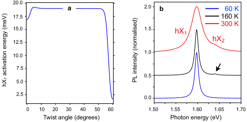
Extended Data Figure 8. Theoretical PL spectra of MoSe2/WS2 for different temperatures. (a) Calculated activation energy for hX1 PL, as a function of twist angle. (b) Normalised PL intensity in the MoSe2 A-exciton energy range, for three different temperatures: and (room temperature). PL from state hX1 produces the peak identified as P1 in our CVD sample measurements. A second peak at higher photon energies (black arrow) is thermally activated at approximately , corresponding to PL from the hX2 state, in excellent agreement with our exfoliated sample measurements (Fig. 5). PL peak broadening and red shift with increasing temperature are not taken into account for these simulations.
Extended Data Figure 9. Twist angle measurements using second harmonic generation (SHG). The symbols show the data for the nearly aligned (a) and misaligned (b) samples fabricated from mechanically exfoliated monolayers. Solid lines in the graph represent the fitting of the data with . All SHG measurements were taken at room temperature using a custom-built system with a Toptica FemtoFErb fs SAM mode-locked laser with a repetition rate of 80 MHz centred at 785 nm. For each measurement, the laser light had a typical incident power of 500 W, was linearly polarized and focused to a spot size of 2 m by a 50x objective lens (NA = 0.36). The SHG signal was separated from the reflected light using a beam splitter and a short-pass filter. A second linear polarizer (analyzer) was placed in the SHG signal path and aligned parallel to the excitation polarization. A motorized half-wave plate was located above the objective and rotated in order to obtain angle resolution. The SHG signal was then measured by a spectrometer and a liquid nitrogen cooled charge-coupled device.
| (eV) | (eV) | (eV) | (meV) | ||
|---|---|---|---|---|---|
| 1.555 (CVD) | 1.756 (CVD) | 1.568 (CVD) | |||
| 1.632 (exfoliated) | 1.854 (exfoliated) | 1.645 (exfoliated) | 26 |
| [] | [] | [meV] | [meV] | |||
|---|---|---|---|---|---|---|
| MoSe2 | 2.20 | |||||
| WS2 | 2.59 |
IX Supplementary Notes
1 Model for intralayer-interlayer exciton hybridization and moiré superlattice minibands for excitons
Bright MoSe2 excitons are formed in an MoSe2/WS2 heterobilayer by valley electrons and holes of opposite spins, where is the valley index. For , the intralayer exciton state is
| (1) |
where [] creates an electron (hole) in the MoSe2 spin– conduction (valence) band, with wave vector near ( gives the A exciton, XA, while gives the B exciton, XB. The same is true for WS2), and is the Fourier transform of the (ground-state) exciton relative-motion wavefunction. and are the electron and hole effective masses; , and is the heterobilayer ground state.
MoSe2 electrons tunnel into the WS2 conduction band through the “hopping term”Wang2016b ,
where and are reciprocal lattice vectors of the corresponding crystals, and represents the in-plane shift between metal atoms in the two layers, which together with the twist angle parametrizes the heterobilayer stacking. The Kronecker delta encodes momentum conservation . Due to symmetry under rotations, the valley is equivalent to (see main text Fig. 3a).
Intralayer MoSe2 excitons can hybridize with interlayer excitons (iXs) of same quantum number , (WS2 electron and an MoSe2 hole)
| (2) |
where is the WS2 electron effective mass and (see Extended Data Table I).
The relative-motion momentum-space wavefunctions of both exciton species are given by
and we obtained the real–space wavefunctions
by solving numerically the two–body problem with bilayer Keldysh–type interactions keldysh ; marcin_bindingenergies_prb_2017 ; mostaani_excitonic_prb_2017 ; complexes2018 ; berkelbach_prb_2013 , finding and from the solutions. Then, we obtain the bright inter–intra exciton mixing term
| (3) |
where ; and ; and , are exciton annihilation operators.
The coupling function decays rapidly with wave vector for macdonald_pnas ; Wang2016b , which allows us to set it as a constant for , and zero otherwise. This makes finite only for and the two other MoSe2 Bragg vectors shown in Extended Data Fig. 3c. For closely aligned () configurations, when , the hopping term gives significant contributions only if and , and is vanishingly small otherwise. Thus, the allowed Bragg vector combinations give
Therefore, to a good approximation,
where we define , with a rotation by and the identity.
For one must choose and for each Bragg vector take , resulting in
From the above analysis, we get for the exciton Hamiltonians
| (4a) | |||
| (4b) |
where
| (5) | |||
with and the spin-orbit couplings of the MoSe2 conduction and valence bands, and the WS2 conduction band spin-orbit coupling. Thus, for , the A- and B-exciton energies can be written as (see Extended Data Table I) and . Analogous terms exist for the valley, given by a time reversal transformation.
The moiré superlattice periodicity, introduced in Eqs. (4a) and (4b) through the terms and , requires that we fold the X and iX bands onto the moiré Brillouin zone,
| (6) | |||
where is limited to the first moiré Brillouin zone (mBZ, Extended Data Fig. 3e). The intra- and interlayer exciton states and hybridize when and
producing hXs states
with corresponding energies .
To evaluate the optical spectra of hX states, we use the light-matter interaction Hamiltonian
Here, creates a photon of in-plane momentum and out-of-plane momentum , and polarization , corresponding to counter-clockwise and clockwise, respectively. We obtain the recombination and absorption rates from Fermi’s golden rule ():
| (7) | |||
For PL, we take into account temperature effects through the Bose-Einstein distribution
where is the energy of the lowest exciton state. The calculated twist-angle dependence of the activation energy for hX1 in MoSe2/WS2, as well as PL spectra at several temperatures, are shown in Extended Data Fig. 8.
2 Harmonic potential approximation to exciton moiré effects in MoSe2/WS2 heterostructures
The moiré superlattice effects on the band structure wallbank ; uchoa and exciton energies macdonald_pnas of bilayer systems, produced by incommensurability and misalignment of the two lattices, are often described in terms of a minimal harmonic potential mcdonald_intra ; hongyi_moire ; Wu2017 . In this section we derive the tunnelling contribution to this potential for intralayer excitons in TMD heterobilayers, using MoSe2/WS2 as a case study. We show that a harmonic potential fails to describe the moiré superlattice effects in the close alignment (anti-alignment) regime in the case of near-resonant exciton bands.
For , interlayer tunnelling allows MoSe2 intralayer excitons to explore the reciprocal lattice of the WS2 layer through virtual tunneling of their electrons onto the WS2 conduction band, and then back onto the MoSe2 conduction band. These virtual processes introduce momentum-dependent corrections to the intralayer exciton energies, which in real space correspond to a potential.
Focusing on the case of , we perform a canonical transformation on the intralayer-interlayer exciton Hamiltonian presented in main text Eq. (4a), with the condition schrieffer_wolff
| (8) |
which removes from all terms that are first order in . A similar procedure is followed for the Hamiltonian of main text Eq. (4b), for . The condition Eq. (8) is achieved by the generator
| (9) |
Evaluating up to second order in we obtain
| (10) |
with the renormalized energies
| (11a) | |||
| (11b) |
The remaining two terms represent scattering by moiré vectors , as shown in Extended Data Fig. 3e. For exciton momenta near the center of the moiré Brillouin zone we have , and we may approximate
| (12a) | |||
| (12b) |
Finally, an inverse Fourier transform gives the harmonic potential for bright intralayer excitons at valley
| (13) |
where , and for convenience we have re-labeled the moiré Bragg vectors as follows: , and . A similar analysis for leads to the potential
| (14) |
Using the values of Extended Data Table I, we find that diverges at , signaling the breakdown of perturbation theory due to a crossing between the intralayer and interlayer exciton bands at the iX band edge, as shown in Extended Data Fig. 2b. Furthermore, Extended Data Fig. 2c shows that, although remains finite for all , the excitation energy in the virtual process becomes smaller than the mixing energy for , indicating that the perturbative approach is no longer valid.
Beyond these angles the intralayer-interlayer exciton mixing strength becomes the dominant energy scale in the problem, such that perturbative methods in general, and a simple description in terms of a potential in particular, cannot describe hX states or the moiré superlattice effects. This is a direct consequence of the near-resonant conduction bands in MoSe2/WS2 heterostructures.
3 Broadening of the photoluminescence line by random fields in the sample
The dependence on twist angle of the emission line broadening shown in Extended Data Fig. 1b may be explained by the coupling of weak electric fields produced by random strain throughout the sample, with the out-of-plane electric dipole of the mixed intralayer-interlayer exciton states. The field-dipole coupling can be estimated as
| (15) |
where and annihilate an electron of momentum and spin projection in MoSe2 and WS2, respectively; is the charge unit, the interlayer distance, and we assume that the out-of-plane electric field is small. In first–order perturbation theory, this gives a correction to the bright, optically–active () mixed exciton energy
| (16) |
where () for (), is the lowest bright hybridized exciton state, and is its interlayer exciton component (see Methods in main text). Excitons in different parts of the sample will experience different values of . Assuming that the values found throughout the sample follow a Gaussian distribution
| (17) |
of mean and variance , the correction will also be normally distributed, with mean value
| (18) |
and a full width at half maximum given by
| (19) |
Allowing for an additive constant, representing the intrinsic broadening of the PL line, we fitted Eq. (19) to the experimental data, and the result is presented in Extended Data Fig. 1b of the main text. The fitting parameters give , or , assuming an approximate interlayer distance of mattheiss_tmds_1973 .
X References
References
- (1) Wang, Y., Wang, Z., Yao, W., Liu, G. B. & Yu, H. Interlayer coupling in commensurate and incommensurate bilayer structures of transition-metal dichalcogenides. Physical Review B 95, 39–41 (2017).
- (2) Keldysh, L. V. Coulomb interaction in thin semiconductor and semimetal films. Soviet Journal of Experimental and Theoretical Physics Letters 29, 658–660 (1979).
- (3) Szyniszewski, M., Mostaani, E., Drummond, N. D. & Fal’Ko, V. I. Binding energies of trions and biexcitons in two-dimensional semiconductors from diffusion quantum Monte Carlo calculations. Physical Review B 95 (2017).
- (4) Mostaani, E. et al. Diffusion quantum Monte Carlo study of excitonic complexes in two-dimensional transition-metal dichalcogenides. Physical Review B 96 (2017).
- (5) Danovich, M. et al. Localized interlayer complexes in heterobilayer transition metal dichalcogenides. Phys. Rev. B 97, 195452 (2018).
- (6) Berkelbach, T. C., Hybertsen, M. S. & Reichman, D. R. Theory of neutral and charged excitons in monolayer transition metal dichalcogenides. Phys. Rev. B 88, 045318 (2013).
- (7) Bistritzer, R. & MacDonald, A. H. Moiré bands in twisted double-layer graphene. Proceedings of the National Academy of Sciences 108, 12233 LP – 12237 (2011).
- (8) Ruiz-Tijerina, D. A. & Fal’ko, V. I. Interlayer hybridization and moiré superlattice minibands for excitons in heterobilayers of transition-metal dichalcogenides. arXiv 1809.09257 (2018).
- (9) Wallbank, J. R., Patel, A. A., Mucha-Kruczyński, M., Geim, A. K. & Fal’Ko, V. I. Generic miniband structure of graphene on a hexagonal substrate. Physical Review B - Condensed Matter and Materials Physics 87 (2013).
- (10) Kindermann, M., Uchoa, B. & Miller, D. L. Zero-energy modes and gate-tunable gap in graphene on hexagonal boron nitride. Physical Review B - Condensed Matter and Materials Physics 86 (2012).
- (11) Wu, F., Lovorn, T. & Macdonald, A. H. Topological exciton bands in moiré heterojunctions. Physical Review Letters 118 (2017).
- (12) Yu, H., Liu, G.-B. B., Tang, J., Xu, X. & Yao, W. Moiré excitons: From programmable quantum emitter arrays to spin-orbit coupled artificial lattices. Science Advances 3, e1701696 (2017).
- (13) Wu, F., Lovorn, T. & MacDonald, A. Theory of optical absorption by interlayer excitons in transition metal dichalcogenide heterobilayers. Physical Review B 97, 035306 (2018).
- (14) Schrieffer, J. R. & Wolff, P. A. Relation between the Anderson and Kondo Hamiltonians. Physical Review 149, 491–492 (1966).
- (15) Mattheiss, L. F. Band structures of transition-metal-dichalcogenide layer compounds. Phys. Rev. B 8, 3719–3740 (1973).
XI Extended Data Figures