Plasmon opens up the possibility to efficiently couple light and matter at sub-wavelength scales. In general, the plasmon frequency is dependent of carrier density. This dependency, however, renders fundamentally a weak plasmon intensity at low frequency, especially for Dirac plasmon (DP) widely studied in graphene. Here we demonstrate a new type of DP, excited by a Dirac nodal-surface state, which exhibits an anomalously density-independent frequency. Remarkably, we predict realization of anomalous DP (ADP) in 1D topological electrides, such as Ba3CrN3 and Sr3CrN3, by first-principles calculations. The ADPs in both systems have a density-independent frequency and high intensity, and their frequency can be tuned from terahertz to mid-infrared by changing the excitation direction. Furthermore, the intrinsic weak electron-phonon coupling of anionic electrons in electrides affords an added advantage of ultra-low phonon-assisted damping and hence a long lifetime of the ADPs. Our work paves the way to developing novel plasmonic and optoelectronic devices by combining topological physics with electride materials.
Anomalous Dirac Plasmons in 1D Topological Electrides
Plasmon, resulting from collective electron density oscillations due to long-range Coulomb interaction, dominates the long-wavelength elementary excitation spectrum in metals and doped semiconductors plasmon1 . It affords an important mechanism to efficiently couple light and matter at sub-wavelength scales, opening up the possibility to manipulate electromagnetic energy in nanophotonic and nano-optoelectronic devices plasmon1 ; plasmon2 ; plasmon3 ; plasmon4 ; plasmon5 ; plasmon6 ; plasmon7 . Recently, Dirac plasmons (DPs), as prototyped in graphene, have attracted great interest, because of their tunable frequency, enhanced light confinement and probable long lifetime graphpla1 ; graphpla2 ; graphpla3 . The typical terahertz (THz) or infrared (IR) response of a DP gives rise to promising applications in spectroscopy, biosensing, and security-related areas graphpla1 ; graphpla2 ; graphpla3 ; graphpla4 ; graphpla5 ; graphpla6 ; graphpla7 .
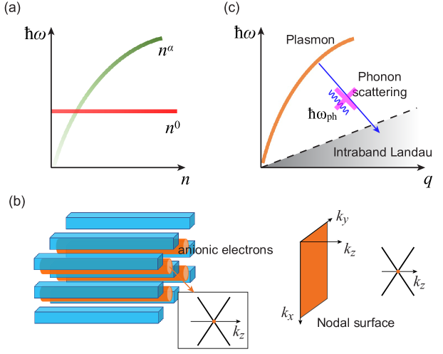
To date, all the known plasmons have a common feature: their frequency strongly depends on carrier density (). For example, the long-wavelength plasmon frequency in metals and graphene follows the and power-law scaling graphpla3 ; graphpla4 , respectively. In addition, the plasmon intensity is proportional to the density of states (DOS) near the Fermi level (), which is also related to . These -dependent features render the conventional DPs to have a weak intensity at low frequency, as illustrated by green line in Fig. 1(a). It poses a fundamental challenge to achieve a strong DP at THz/IR frequency.
In this Letter, we demonstrate an anomalous DP (ADP), excited by a unique Dirac nodal-surface (DNS) state, which exhibits a surprising -independent frequency and a constant high intensity. Most remarkably, we predict the existence of ADP in 1D topological electrides, where the DNS states are formed by anionic electrons trapped in the cavities. In addition, the loosely bound anionic electrons in electrides results in an ultra-weak phonon scattering and hence a long lifetime of the ADPs. Importantly, we further discover that Ba3CrN3 and Sr3CrN3 are ideal 1D topological electrides to realize the ADPs, having a tunable frequency from THz to mid-IR and an ultra-low phonon-assisted damping for a very long lifetime.
The classical long-wavelength plasmon frequency in 3D metals is written as , where and is the effective mass and dielectric constant, respectively. Recently, the emerging topological semimetal (TSM) states tsm1 ; tsm2 ; tsm3 ; tsm4 in solids, as characterized by a linear band crossing between conduction and valence bands in higher dimensions (i.e., 1D and 2D), provide a new platform to create novel DPs beyond graphene diracpla ; nodelinepla1 ; nodelinepla2 ; diracplaexp . For a TSM, the “relativistic” effective mass of quasiparticles is -dependent, as and for Dirac nodal-point (DNP) and Dirac nodal-line (DNL) semimetals, respectively SM . Consequently, the scaling in the classical plasmon frequency is partially offset by the , resulting in and for DNP and DNL semimetals, respectively diracpla ; nodelinepla1 ; nodelinepla2 . Interestingly, we realize when the dimensionality of band crossing is further increased from 1D DNL to 2D DNS dns1 ; dns2 , becomes proportional to , , to completely offset the scaling in the frequency. This means that the plasmon frequency of a DNS semimetal becomes independent of , which is fundamentally different from all the known plasmons.
To show this vigorously, based on random phase approximation (RPA) and irreducible polarizability of Dirac systems diracpla , one can deduce the long-wavelength plasmon frequency for DNS state as SM
| (1) |
where is the degeneracy factor, is the DNS area in the momentum space, is the Fermi velocity along the normal direction of DNS, and is the angle between and the normal direction of DNS. As shown by the red line in Fig. 1(a), the long-wavelength plasmon of DNS follows exactly a scaling. Moreover, the 1D nature of DNS leads to a constant high DOS near SM , which produces a constant strong plasmon intensity. Consequently, an ADP has inherently a -independent frequency and high intensity. As indicated by Eq. (1), the frequency of ADP depends solely on the direction of plasmon excitation (a function), providing a simple way to continuously tune its frequency.
Though the DNS states were proposed theoretically dns1 ; dns2 , they have not been observed in experiments due to the lack of ideal materials. Here we predict that the DNS states and ADPs can be realized in 1D topological electrides. Electrides are known as special ionic solids, in which excess electrons are trapped in the cavities to serve as anions electride1 ; electride2 ; electride3 ; electride4 . Generally, they can be classified into 2D, 1D and 0D electrides according to the dimensionality of the confinement electride5 . The anionic electrons have a low work function, because they are rather loosely bound to atoms or lattice. As a result, they may appear as occupied states near , suitable for band inversion or band crossing topoelectride . As shown in Fig. 1(b), when the anionic electrons are confined in 1D channels (e.g., direction), they might generate a band crossing along direction in the momentum space. Their inter-channel coupling in periodic array translates the crossing points along the and directions in the 3D Brillouin zone (BZ). The resulting 2D band crossing can be protected by some specific crystal symmetries to realize a DNS state. In addition, differing from the conventional topological materials, there is a negligible spin-orbit coupling (SOC) effect for loosely bound anionic electrons, which is also vital for achieving the spinless nodal states.
We note that the nature of electrides also naturally makes the excited ADP to have a low damping. In general, there are several possible damping pathways for plasmons damping1 , including direct decay into electron-hole pairs via intra- or inter-band Landau damping, scattering from impurities or defects, and inelastic scattering with phonons. For DPs, the first two processes can be effectively reduced by changing and improving sample quality, respectively. Thus, the phonon-assisted damping is usually the dominant loss pathway damping1 ; damping2 ; damping3 . As shown in Fig. 1(c), a DP can decay into an electron-hole pair via emission of a phonon. Here for our proposed ADPs in electrides, the loosely bound anionic electrons generally exhibit a weak electron-phonon (e-ph) coupling with a negligible phonon scattering Ca2Ne-ph . Consequently, the phonon-assisted damping pathway can be largely suppressed.
The above analysis indicates that an ADP generated by a DNS state in 1D electrides could overcome both low intensity and phonon-assisted damping associated with the conventional DPs. Based on an extensive structural search in the ICSD database, we successfully identify that Ba3CrN3 and Sr3CrN3 are ideal 1D electrides to realize the desired ADP.
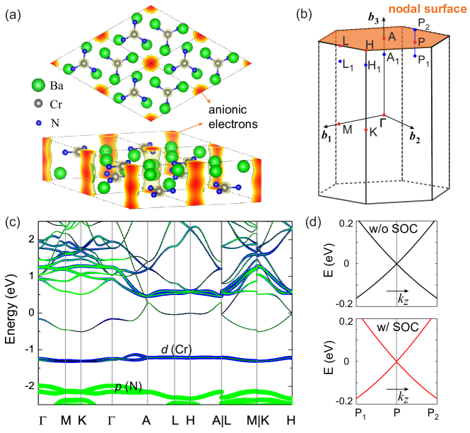
Ba3CrN3 and Sr3CrN3 have already been synthesized in experiments expstruc . Here we take Ba3CrN3 as an example to illustrate its ADP excitations, and leave the results of Sr3CrN3 in the Supplementary Information SM . As shown in Fig. 2(a), the unit cell of hexagonal Ba3CrN3 (space group ) contains two trigonal planar CrN3 anions that are related to each other by an inversion or screw rotation symmetry expstruc . Along the direction, a 1D cavity is formed at the corner of the unit cell. Our calculations indicate that Ba3CrN3 is nonmagnetic with zero magnetic moment on Cr atoms. This is because Cr has a charge state, and its remaining two electrons fill a singlet state. Thus, there are two “excess” electrons remaining per unit cell to act as “anions”. The band structure along high-symmetry lines in BZ [Fig. 2(b)] is shown in Fig. 2(c), which indicates a semi-metallic feature of Ba3CrN3. Strikingly, the two energy bands near are mostly contributed by the anionic electrons with negligible atomic orbital components. The band dispersions are small in the and planes but large along the direction, indicating a 1D nature. The partial charge densities of these two bands around further show that the anionic electrons are confined in the channels of 1D cavity [Fig. 2(a)]. Hence, Ba3CrN3 is a 1D electride with an effective formula [Ba6Cr2N6].
Figure 2(c) also shows that the conduction and valence bands are degenerate along the high-symmetry paths –––, but split along –, –, and –. Actually, such band degeneracy occurs at all points in the plane, as confirmed by plotting the bands [Fig. 2(d)] along an arbitrary line –– perpendicular to the plane at an arbitrary point in the plane [see Fig. 2(b)]. So, the band crossing takes place throughout the BZ boundary to form a perfect DNS state [orange plane in Fig. 2(b)].
The DNS state is protected by a nonsymmorphic symmetry dns1 . Ba3CrN3 has time-reversal symmetry , with being the complex conjugation, inversion symmetry , and screw rotation symmetry , combining a twofold rotation and a half-lattice translation along the axis. Two compound symmetries, and , are preserved in the plane, and their anticommutation ensures the twofold band degeneracy in the entire plane dns1 . When SOC effect is included, this degeneracy of DNS is lifted but the SOC gap is negligibly small due to the unique nature of anionic electrons [see Fig. 2(d)]. The similar conclusions are drawn for Sr3CrN3 SM .

After establishing an ideal DNS state in Ba3CrN3, we set to investigate its plasmonic excitations. Under RPA, the collective plasmon mode can be determined by the dynamical dielectric function , where is the Coulomb interaction in the wave vector space, and is the irreducible polarizability function. In the long-wavelength limit (), a noninteracting irreducible polarizability is given by diracpla ; Siplasmon
| (2) |
where is the Fermi-Dirac distribution function. The collective plasmon mode is defined at zeros of the complex dynamical dielectric function. It is more convenient to calculate the electron energy loss spectrum (EELS), i.e., EELS=Im, whose broadened peaks indicate the plasmons Siplasmon . Along the direction, we calculate the long-wavelength ( = 0.001 Å-1) dielectric function of Ba3CrN3 and EELS at 300 K, as shown in Fig. 3(a). It can be seen that a sharp plasmon peak with high intensity appears for Re. Simultaneously, the Im, indicating a weak direct damping rate. The plasmon excitation energy of 0.125 eV corresponds to a frequency of THz in the mid-IR range. As shown in Fig. 3(b), the calculated plasmon dispersion of Ba3CrN3 over a small range of wave vector has a normal relationship because of a 3D dielectric screening. Importantly, the plasmon excitations lie above the region of intraband Landau damping, consistent with the sharp peak of plasmon; it indicates that the direct decay into electron-hole pairs is almost forbidden.
In Fig. 3(c), we plot the plasmon frequency as a function of density and excitation direction angle at the long-wavelength limit. Remarkably, at any fixed excitation direction, the plasmon frequency keeps a constant value () for a significantly large range of changing density up to cm-3 (i.e., within the energy range of linear band dispersion SM ), consistent with our predicted feature of ADP. Meanwhile, a high intensity of ADP remains almost unchanged for different SM , because of a constant DOS within the same energy range. On the other hand, the ADP frequency depends on plasmon direction and can be continuously tuned, following a function [black curve in Fig. 3(c)], which agrees well with our model [Eq. (1)]. It is noted that the plasmon mode along the direction (i.e., ) has a small excitation energy ( meV) and enters the particle-hole continuum at a large SM . While the non-zero frequency for is due to the fact that the entire DNS band has a small dispersion in the plane. Moreover, the high intensity of ADP almost maintains for different plasmon directions, as confirmed by our calculations SM . As a result, by changing , a high-intensity ADP with a frequency tuned from THz to mid-IR can be achieved [Fig. 3(c)]. In addition, we find the plasmon frequency is robust against strain, due to the nature of loosely bound anionic electrons SM .
Finally, we discuss the phonon scattering of ADPs in Ba3CrN3, by calculating the e-ph interaction for the DNS states. The electron linewidth or scattering rate is directly connected to the imaginary part of the e-ph self-energy e-ph1
| (3) | ||||
where is the phonon energy, () is the Bose-Einstein (Fermi-Dirac) distribution, and is the e-ph coupling matrix element corresponding to electron scattering from band at to band at by phonon with . Here, a Wannier-Fourier interpolation method epw is used to obtain the numerical results of e-ph coupling.
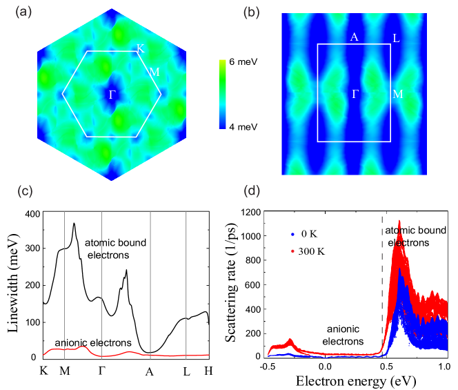
In Figs. 4(a) and (b), we plot -dependent average e-ph coupling matrix element of all 42 phonon modes for electron scattering from the DNS band at the point of BZ. It is found that the e-ph interactions are indeed ultra-weak and the average coupling matrix element is about several meV, which is two orders of magnitude smaller than that of graphene graphe-ph . Similar results are obtained at the other momentum points SM . The calculated electron linewidths for the occupied DNS band of anionic electrons and for an unoccupied band of atomic bound electrons are shown in Fig. 4(c). Remarkably, the former is much smaller than the latter over the entire BZ. Correspondingly, the scattering rate of anionic electrons at low energy is much lower than that of atomic bound electrons at high energy, as shown in Fig. 4(d). As a result, the relaxation time is very long (e.g., about 30 fs at 300 K) for the DNS states, even longer than that of graphene plasmons damping2 . According to Eq. (3), the scattering rate is related to both the e-ph coupling matrix elements and the DOS. The low electron scattering of graphene is mostly contributed by the low DOS near , while the carrier doping will inevitably result in a rapid increase of scattering rate graphe-ph . In contrast, the ultra-weak e-ph coupling and nearly constant DOS exist in a wide energy range for Ba3CrN3, which leads to an ultra-low phonon scattering rate over a large range of doping [Fig. 4(d)].
In conclusion, we demonstrate an ADP realized by exciting a DNS state in 1D electride, as exemplified in Ba3CrN3 and Sr3CrN3. It exhibits an anomalous density-independent frequency, which enables a low-frequency plasmon with high intensity. Furthermore, the weak e-ph interaction in electride materials reduces the phonon-assisted damping of ADP, leading to long-lived plasmons. Our work paves the way to developing plasmonic applications by combining topological states with electride materials, which are expected to draw broad interests especially from experimentalists.
J. Wang and X. Sui contributed equally to this work. The authors thank L. Kang and X. Zhang for helpful discussions. J.W. and B.H. acknowledge the support from NSFC (Grant No. 11574024) and NSAF U1530401. X.S. and W.D. acknowledge support from MOST of China (Grant No. 2016YFA0301001) and NSFC (Grants No. 11674188 and No. 11334006). F.L. acknowledge the support from US-DOE (Grant No. DE-FG02-04ER46148). Part of the calculations were performed at Tianhe2-JK at CSRC.
References
- (1) S. A. Maier, Plasmonics: Fundamentals and Applications (Springer, New York, 2007).
- (2) W. L. Barnes, A. Dereux, and T. W. Ebbesen, Surface plasmon subwavelength optics, Nature 424, 824 (2003).
- (3) E. Ozbay, Plasmonics: Merging Photonics and Electronics at Nanoscale Dimensions, Science 311, 189 (2006).
- (4) D. K. Gramotnev and S. I. Bozhevolnyi, Plasmonics beyond the diffraction limit, Nat. Photon. 4, 83 (2010).
- (5) S. Lal, S. Link, and N. J. Halas, Nano-optics from sensing to waveguiding, Nat. Photon. 1, 641 (2007).
- (6) H. A. Atwater and A. Polman, Plasmonics for improved photovoltaic devices, Nat. Mater. 9, 205 (2010).
- (7) C. Clavero, Plasmon-induced hot-electron generation at nanoparticle/metal-oxide interfaces for photovoltaic and photocatalytic devices, Nat. Photon. 8, 95 (2014).
- (8) F. Bonaccorso, Z. Sun, T. Hasan, and A. C. Ferrari, Graphene photonics and optoelectronics, Nat. Photon. 4, 611 (2010).
- (9) F. H. L. Koppens, D. E. Chang, and F. J. García de Abajo, Graphene plasmonics: a platform for strong light-matter interactions, Nano Lett. 11, 3370 (2011).
- (10) L. Ju, B. Geng, J. Horng, C. Girit, M. Martin, Z. Hao, H. A. Bechtel, X. Liang, A. Zettl, Y. R. Shen, and F. Wang, Graphene plasmonics for tunable terahertz metamaterials, Nat. Nanotech. 6, 630 (2011).
- (11) A. N. Grigorenko, M. Polini, and K. S. Novoselov, Graphene plasmonics, Nat. Photon. 6, 749 (2012).
- (12) Z. Fei, et al., Gate-tuning of graphene plasmons revealed by infrared nanoimaging, Nature 487, 82 (2012).
- (13) J. Chen, et al., Optical nano-imaging of gate-tunable graphene plasmons, Nature 487, 77 (2012).
- (14) D. Rodrigo, O. Limaj, D. Janner, D. Etezadi, F. J. García de Abajo, V. Pruneri, and H. Altug, Mid-infrared plasmonic biosensing with graphene, Science 349, 165 (2015).
- (15) C.-K. Chiu, J. C. Y. Teo, A. P. Schnyder, and S. Ryu, Classification of topological quantum matter with symmetries, Rev. Mod. Phys. 88, 035005 (2016).
- (16) N. P. Armitage, E. J. Mele, and A. Vishwanath, Weyl and Dirac semimetals in three-dimensional solids, Rev. Mod. Phys. 90, 015001 (2018).
- (17) A. A. Burkov, M. D. Hook, and Leon Balents, Topological nodal semimetals, Phys. Rev. B 84, 235126 (2011).
- (18) H. Weng, X. Dai, and Z. Fang, Topological semimetals predicted from first-principles calculations, J. Phys.: Condens. Matter 28, 303001 (2016).
- (19) S. D. Sarma and E. H. Hwang, Collective modes of the massless Dirac plasma, Phys. Rev. Lett. 102, 206412 (2009).
- (20) Z. Yan, P.-W. Huang, and Z. Wang, Collective modes in nodal line semimetals, Phys. Rev. B 93, 085138 (2016).
- (21) J.-W. Rhim and Y. B. Kim, Anisotropic density fluctuations, plasmons, and Friedel oscillations in nodal line semimetal, New J. Phys. 18, 043010 (2016).
- (22) A. Politano, G. Chiarello, B. Ghosh, K. Sadhukhan, C.-N. Kuo, C. S. Lue, V. Pellegrini, and A. Agarwal, 3D Dirac Plasmons in the Type-II Dirac Semimetal PtTe2, Phys. Rev. Lett. 121, 086804 (2018).
- (23) See Supplemental Material for details of three different 3D topological semimetals (DNP, DNL, and DNS) and their plasmon excitation derivations, computational methods, electronic and plasmonic properties of Ba3CrN3 and Sr3CrN3, and e-ph coupling calculation tests of Ba3CrN3, which also includes Refs. [19,21,24–34].
- (24) G. Kresse and J. Furthmüller, Efficiency of ab-initio total energy calculations for metals and semiconductors using a plane-wave basis set, Comput. Mater. Sci. 6, 15 (1996).
- (25) G. Kresse and J. Furthmüller, Efficient iterative schemes for ab initio total-energy calculations using a plane-wave basis set, Phys. Rev. B 54, 11169 (1996).
- (26) P. E. Blöchl, Projector augmented-wave method, Phys. Rev. B 50, 17953 (1994).
- (27) J. P. Perdew, K. Burke, and M. Ernzerhof, Generalized Gradient Approximation Made Simple, Phys. Rev. Lett. 77, 3865 (1996).
- (28) M. G. Barker, M. J. Begley, P. P. Edwards, D. H. Gregory, and S. E. Smith, Synthesis and crystal structures of the new ternary nitrides Sr3CrN3 and Ba3CrN3, J. Chem. Soc. (Dalton Trans.) 1, 1 (1996).
- (29) N. Marzari and D. Vanderbilt, Maximally localized generalized Wannier functions for composite energy bands, Phys. Rev. B 56, 12847 (1997).
- (30) I. Souza, N. Marzari, and D. Vanderbilt, Maximally localized Wannier functions for entangled energy bands, Phys. Rev. B 65, 035109 (2001).
- (31) F. Giustino, M. L. Cohen, and S. G. Louie, Electron-phonon interaction using Wannier functions, Phys. Rev. B 76, 165108 (2007).
- (32) S. Poncé, E. R. Margine, C. Verdi, and F. Giustino, EPW: Electron-phonon coupling, transport and superconducting properties using maximally localized Wannier functions, Comput. Phys. Comm. 209, 116 (2016).
- (33) P. Giannozzi, S. Baroni, N. Bonini, M. Calandra, R. Car, C. Cavazzoni, D. Ceresoli, G. L Chiarotti, and M. Cococcioni, QUANTUM ESPRESSO: a modular and open-source software project for quantum simulations of materials, J. Phys.: Condens. Matter 21, 395502 (2009).
- (34) K. M. Borysenko, J. T. Mullen, E. A. Barry, S. Paul, Y. G. Semenov, J. M. Zavada, M. Buongiorno Nardelli, and K. W. Kim, First-principles analysis of electron-phonon interactions in graphene, Phys. Rev. B 81, 121412(R) (2010).
- (35) Q.-F. Liang, J. Zhou, R. Yu, Z. Wang, and H. Weng, Node-surface and node-line fermions from nonsymmorphic lattice symmetries, Phys. Rev. B 93, 085427 (2016).
- (36) W. Wu, Y. Liu, S. Li, C. Zhong, Z.-M. Yu, X.-L. Sheng, Y. X. Zhao, and S. A. Yang, Nodal surface semimetals: Theory and material realization, Phys. Rev. B 97, 115125 (2018).
- (37) J. L. Dye, Electrides: Ionic Salts with Electrons as the Anions, Science 247, 663 (1990).
- (38) J. L. Dye, Electrons as Anions, Science 301, 607 (2003).
- (39) S. Matsuishi, Y. Toda, M. Miyakawa, K. Hayashi, T. Kamiya, M. Hirano, I. Tanaka, H. Hosono, High-Density Electron Anions in a Nanoporous Single Crystal: [CaAlO]4+(4), Science 301, 626 (2003).
- (40) K. Lee, S. W. Kim, Y. Toda, S. Matsuishi, H. Hosono, Dicalcium Nitride as a TwoDimensional Electride with an Anionic Electron Layer, Nature 494, 336 (2013).
- (41) L. A. Burton, F. Ricci, W. Chen, G.-M. Rignanese, G. Hautier, High-Throughput Identification of Electrides from all Known Inorganic Materials, Chem. Mater. 30, 7521 (2018).
- (42) M. Hirayama, S. Matsuishi, H. Hosono, and S. Murakami, Electrides as a New Platform of Topological Materials, Phys. Rev. X 8, 031067 (2018).
- (43) H. Buljan, M. Jablan, and M. Soljačić, Damping of plasmons in graphene, Nat. Photon. 7, 346 (2013).
- (44) H. Yan, T. Low, W. Zhu, Y. Wu, M. Freitag, X. Li, F. Guinea, P. Avouris, and F. Xia, Damping pathways of mid-infrared plasmons in graphene nanostructures, Nat. Photon. 7, 394 (2013).
- (45) A. Woessner, M. B. Lundeberg, Y. Gao, A. Principi, P. A. González, M. Carrega, K. Watanabe, T. Taniguchi, G. Vignale, M. Polini, J. Hone, R. Hillenbrand, and F. H. L. Koppens, Highly confined low-loss plasmons in graphene-boron nitride heterostructures, Nat. Mater. 14, 421 (2015).
- (46) X. Zeng, S. Zhao, Z. Li, and J. Yang, Electron-phonon interaction in a Ca2N monolayer: Intrinsic mobility of electrene, Phys. Rev. B 98, 155443 (2018).
- (47) Z. F. Wang and F. Liu, Self-Assembled Si(111) Surface States: 2D Dirac Material for THz Plasmonics, Phys. Rev. Lett. 115, 026803 (2015).