Erasing odd-parity states in semiconductor quantum dots coupled to superconductors
Abstract
Quantum dots are gate-defined within InSb nanowires, in proximity to NbTiN superconducting contacts. As the coupling between the dot and the superconductor is increased, the odd-parity occupations become non-discernible (erased) both above and below the induced superconducting gap. Above the gap, conductance in the odd Coulomb valleys increases until the valleys are lifted. Below the gap, Andreev bound states undergo quantum phase transitions to singlet ground states at odd occupancy. We observe that the apparent erasure of odd-parity regimes coincides at low-bias and at high-bias. This observation is reproduced in numerical renormalization group simulations, and is explained qualitatively by a competition between Kondo temperature and the induced superconducting gap. In the erased odd-parity regime, the quantum dot exhibits transport features similar to a finite-size Majorana nanowire, drawing parallels between even-odd dot occupations and even-odd one-dimensional subband occupations.
The prospect of topological quantum computing has motivated recent studies of charge parity, which is an observable that can distinguish the states of a Majorana quantum bit Das Sarma et al. (2015). Experiments have demonstrated that electrons can be added to small superconducting islands either in pairs or one at a time, depending on the interplay of energy scales of the system Tuominen et al. (1992); Eiles et al. (1993); Lafarge et al. (1993); Albrecht et al. (2016). Quantum jumps of parity have been observed in superconducting circuits Janvier et al. (2015); Hays et al. (2018). In quantum dots coupled to superconductors, a quantum phase transition (QPT) between odd- and even-parity ground states has been investigated theoretically Matsuura (1977); Satori et al. (1992); Yoshioka and Ohashi (2000); Choi et al. (2004); Oguri and Tanaka (2004); Bauer et al. (2007); Karrasch et al. (2008) and experimentally Eichler et al. (2007); Sand-Jespersen et al. (2007); Buizert et al. (2007); Grove-Rasmussen et al. (2009); Deacon et al. (2010); Kanai et al. (2010); Pillet et al. (2010); Maurand et al. (2012); Chang et al. (2013); Kumar et al. (2014); Lee et al. (2014); Jellinggaard et al. (2016); Lee et al. (2017).
In this paper, we study the transition from the closed to the open regime (i.e., weak hybridization to strong hybridization regime) in a quantum dot defined in a semiconductor nanowire with superconducting contacts. We demonstrate how the transport signatures of odd-parity quantum-dot states are erased in the open dot regime. At high source-drain bias, we observe a transition from well-defined Coulomb diamonds to a conductance modulation pattern in which odd Coulomb valleys rise in conductance faster than the even valleys. We explain this based on Kondo physics playing a role at stronger coupling. At low bias, we observe Andreev bound states (ABS) that cross zero energy at every change in ground state parity from even to odd, while in the open regime the ABS do not cross zero bias. This is the manifestation of a well-studied QPT upon which the system always stays in a many-body singlet ground state.
Interestingly, we notice that the ABS QPT at low bias coincides with the lifting of the odd Coulomb valleys at high bias. We furthermore reproduce this observation qualitatively in the simulation of the Anderson impurity model using the numerical renormalization group (NRG). We argue that this coincidence is expected because both high-bias and low-bias features are determined by the competition between the Kondo temperature and the induced gap.
In the same system we furthermore find similarities between the evolution of ABS and the emergence of Majorana bound states (MBS). Specifically, the phase diagram of the ABS QPT in gate voltage and magnetic field is reminiscent of the phase diagram predicted for the topological superconducting phase, if even-odd dot occupations are replaced with even-odd subband occupations. This highlights the persistent need to identify truly unique signatures of MBS and to deeper study the related regime of trivial ABS.
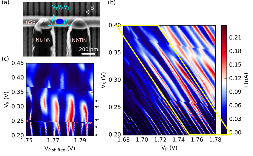
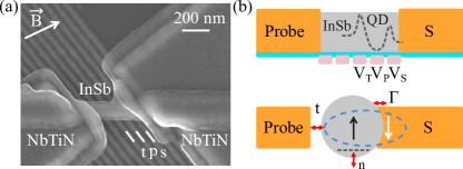
InSb nanowires are grown using metalorganic vapor phase epitaxy (MOVPE) and transferred onto metallic gate patterns which are lines with 60-80 nm center-to-center pitch. The gates are covered by 10 nm of HfO2 dielectric. NbTiN superconducting contacts are fabricated on top of the nanowire. The device in Fig.1(a) is highly tunable: previous reports on the same device demonstrated that it can be used to set up a quantum dot near the left or the right superconductor, as well as a double dot Su et al. (2017, 2018). Here a single quantum dot is defined using gates , , near the right superconductor. The barrier controlled by gate is set near pinch off, defining the left contact as the tunnel probe. Even though the probe contact is a superconductor, the soft gap effect introduces finite density of states at the Fermi level. This makes the low bias spectra similar to those obtained with a normal probe Su et al. (2018). The barrier controlled by the voltage on gate tunes , the coupling to the right superconductor (Fig.1(b)). The voltage on gate , , primarily controls the dot chemical potential or the number of electrons . The minimal 2-terminal resistance of the device is 4 k. Measurements are performed in a dilution refrigerator with a base temperature of 40 mK.
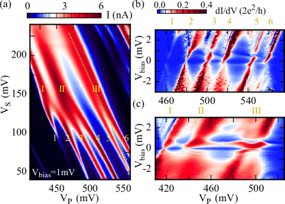
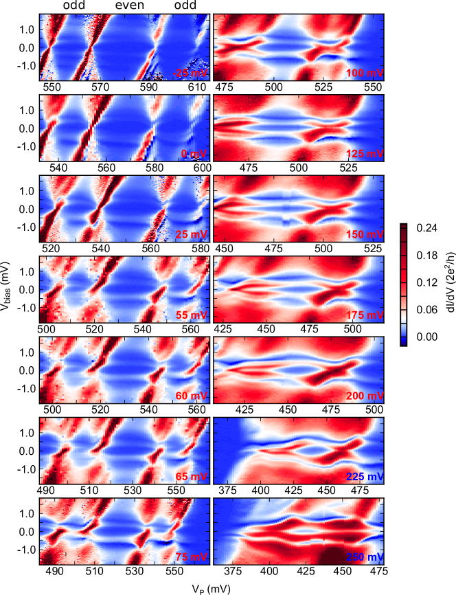
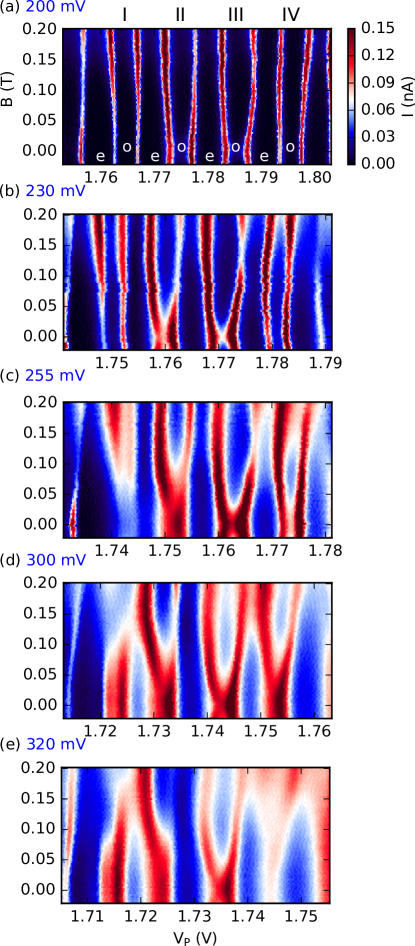
The key experimental observations of the paper are presented in Figs. 2 and 3. For we observe a sequence of Coulomb peaks by tuning ; we label these peaks 1 through 6 in Figs. 2(a,b). For Coulomb peaks are seen continuously merging pairwise into broader resonances labeled ’I’, ’II’, ’III’ in Figs. 2(a, c). Fig. 2(a) is obtained under a source drain bias voltage , above the apparent induced gap. It shows that current in every other Coulomb valley increases with higher , i.e. the odd valleys are being lifted. The effect of transitioning from to conductance pattern in open quantum dots can be qualitatively understood as follows. By making the tunneling barrier more transparent, the effect of the Coulomb interaction on the dot is suppressed: at very high hybridization the Coulomb energy becomes irrelevant and the system behaves as if no additional energy were required to add a second electron to the same quantum dot orbital state Steele et al. .
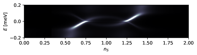
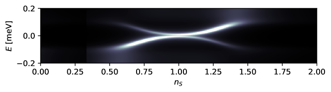
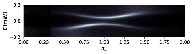
At lower biases, a set of horizontal resonances near is observed (Figs. 2(b,c)). In Fig. 2(b), the horizontal resonances appear to coexist with Coulomb resonances 1-6. Such resonances have been reported in quantum dots with superconducting contacts and are either related to co-tunneling enhanced by high density of states at the gap edge Grove-Rasmussen et al. (2009), or related to ABS in the dot. In Fig. 2(c), at higher , when the quantum dot is stronger coupled to the right superconductor, the horizontal resonances are still present, but the Coulomb peaks are absent. Instead, at zero bias conductance exhibits a local minimum throughout the range of . At high bias, Coulomb diamonds are replaced with three broader resonances I,II,III.
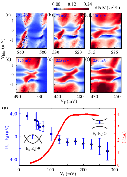
The detailed evolution of low-bias superconductivity-related resonances as a function of is shown in Figs. 3(a)-(f), which is focusing on the region labeled ’III’ in Fig. 2. For low (panels (a)-(b)) the resonances form a loop around zero bias. The loop shrinks with increasing until the two zero-bias crossings merge around (panel (c)). For higher , the horizontal resonances at positive and negative biases exhibit an anticrossing, its level repulsion growing with more positive (panels (d),(e),(f)). This transition from loop-like to anticrossing-like resonances has been previously studied as a manifestation of the singlet-doubled QPT at odd quantum dot occupancy Martín-Rodero and Levy Yeyati (2011); Luitz et al. (2012); Lee et al. (2017); Meden (2018). Supplemental materials contain comprehensive data on the evolution from the closed to open dot regime over wider ranges of and .
In Fig. 3(g) we correlate the lifting of the odd Coulomb valley ’III’ with the singlet-doublet ABS QPT. To identify the valley-lifting point, we plot in solid line a trace of current along a green dashed line in Fig. 2(a) at . When is low, the current is near zero because of Coulomb blockade. As is increased, the dot becomes open and the current starts to increase and finally reaches .
To identify the singlet-doublet transition, we plot the bias voltage of the lowest positive resonance in the center of region ’III’ which corresponds to the energy difference between the singlet and the doublet states (, see diagrams in Fig. 3(g)). We assign positive values of to loop-like resonances (doublet ground state) and negative values to anticrossing-like resonances (singlet ground state). The data show that the lifting of Coulomb valleys and the singlet-doublet QPT occur within the same range of . In other words, the signatures of odd-parity regimes are erased from transport data at similar dot parameters, both above and below the induced superconducting gap. These results are reproduced in another device, see supplemental materials. We note that the normal-state tunneling amplitude, a useful scaling parameter, cannot be extracted from these data in a way similar to Ref.Lee et al., 2017 because superconductivity cannot be suppressed due to the high critical temperature and field of NbTiN. Also, is be below the bulk gap of NbTiN, however, the gap is soft in this device meaning there is a finite single-particle density of states at all energies.
In order to numerically analyze the observed experimental coincidence presented in Fig. 3(g), we describe the quantum dot using the single-impurity Anderson model:
| (1) |
where is the quantum-dot level, is the dot occupancy, is the electron-electron repulsion parameter, are the tunneling amplitudes between the dot and the superconducting lead. The coupling between the dot and the lead is quantified by the hybridization strength , where is the normal-state density of states in the electrode. The lead is described by a Bardeen-Cooper-Schrieffer (BCS) Hamiltonian with the gap . In addition, we take into account that the proximitized gap in the quantum dot is soft. The complete information about the lead is contained in the hybridization function in the Nambu formalism. For a BCS Hamiltonian it takes the form
| (2) |
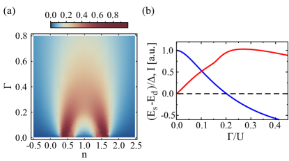
To describe a hard induced gap, one uses the argument . To model a soft-gap situation, one instead uses where is the finite life-time of Bogoliubov quasiparticles: this smoothens the BCS coherence peaks as well as produces a finite density of states inside the gap. We study the spectral and transport properties of this model using the NRG method Wilson (1975); Bulla et al. (2008); Pillet et al. (2013), which consists of discretizing the continuum of states in the leads, transforming the problem into a tight-binding chain form, and iteratively diagonalizing the resulting Hamiltonian. The Wilson chain coefficients that correspond to the generalized BCS hybridization can be computed using the artifact-less discretization scheme Žitko (2009) generalized to the matrix case Jin-Guo Liu (2016). The spectral function is computed using the density-matrix NRG algorithm. We used model parameters , , systematically sweeping and . The energy unit is half-bandwidth, . The calculations were performed with the NRG discretization parameter by averaging over interleaved discretization grids.
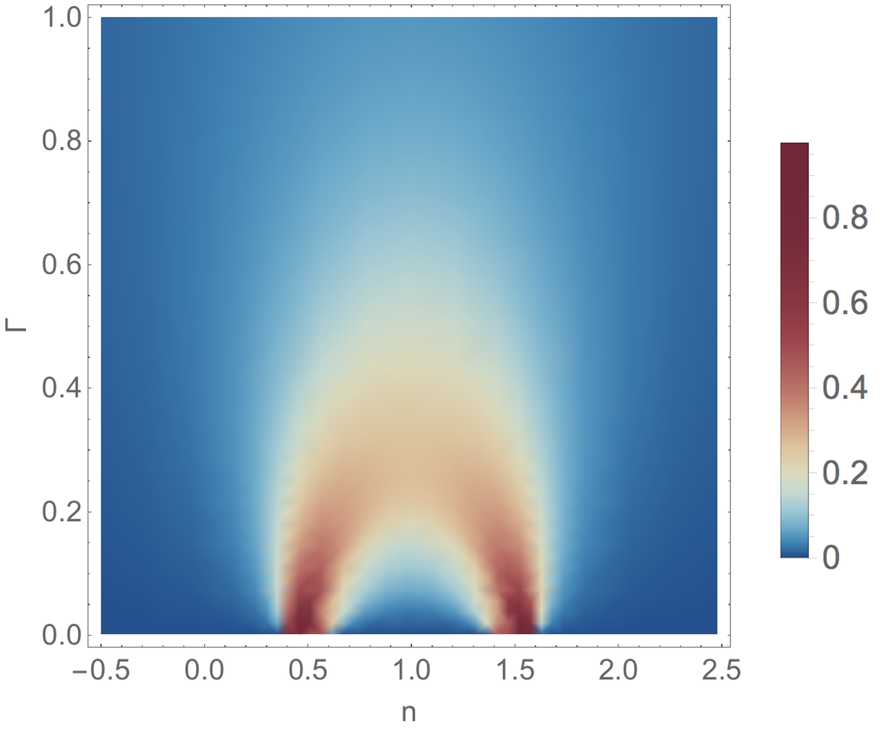
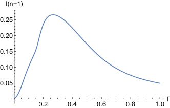
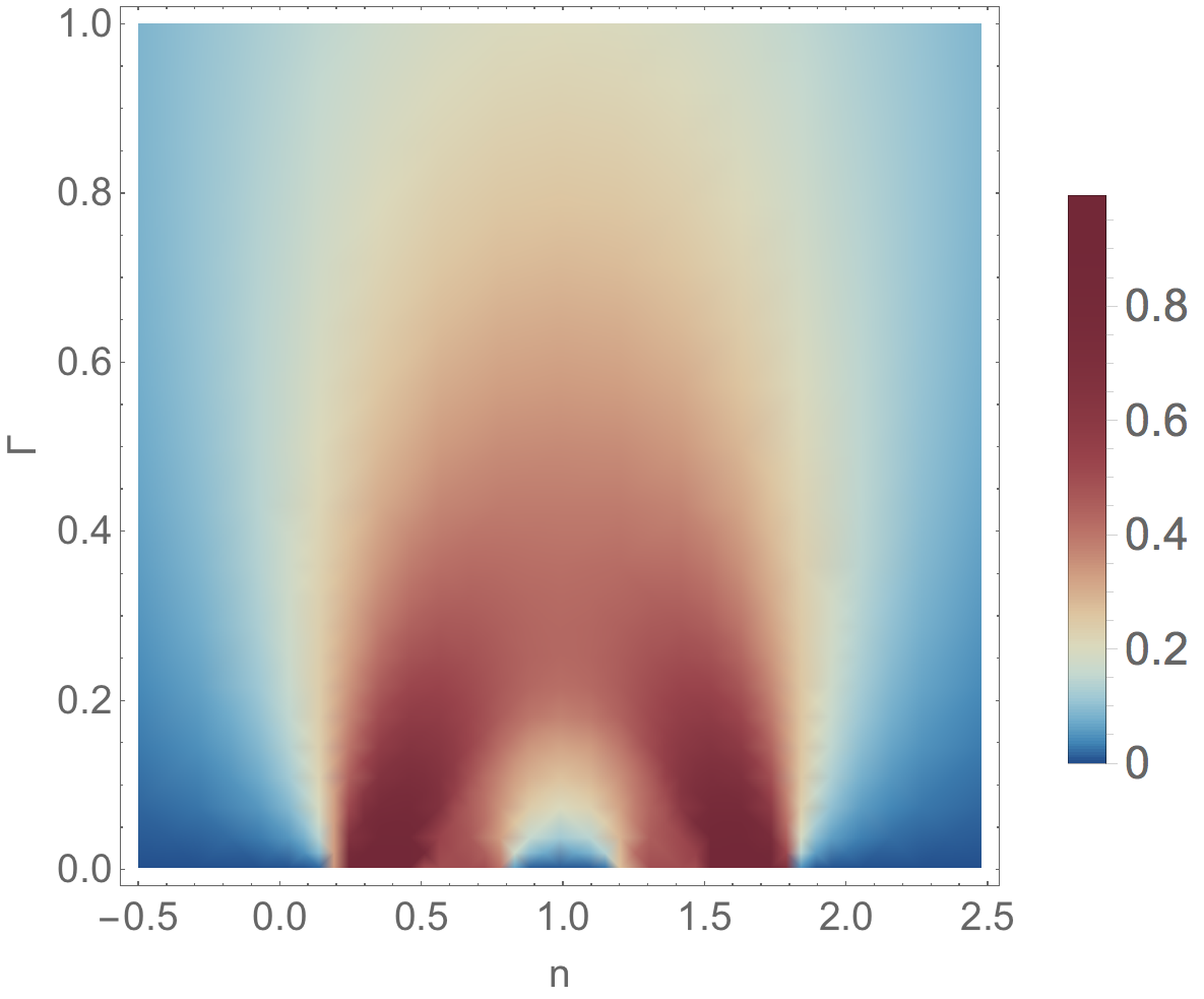
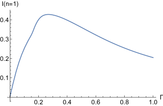
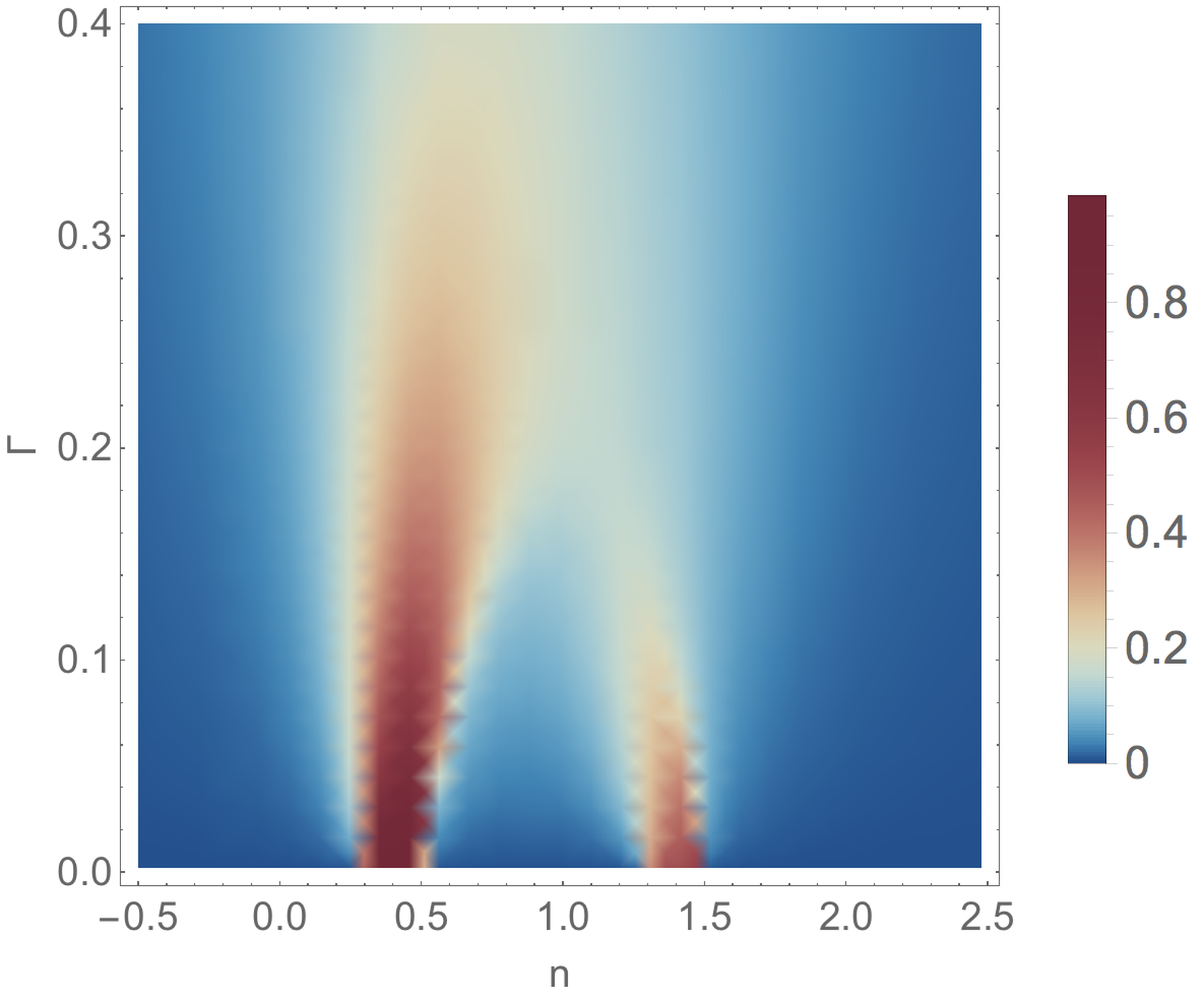
To approximate the experimental finite-bias transport current within our model we compute an integral of the quantum dot spectral function in the spirit of the Meir-Wingreen formalism, neglecting any possible non-equilibrium effects, from to . These results are shown in Fig. 4(a) as a function of the ’p’ gate (converted to units of quantum dot charge ) and the contact barrier (expressed as hybridization strength ). The results can be interpreted based on the established knowledge about the transport through quantum dots with normal-state leads, taking into account that the gap terminates the renormalization of the exchange coupling, thus it plays a similar role as the temperature in the normal-state case. Such mapping is possible, because the bias voltage is significantly larger than the gap and similar transport processes are relevant as in the normal state. Hence, in the weak coupling regime, where , the current is high only at the charge degeneracy points ( and ) due to Coulomb blockade physics relevant in the regime. As the coupling increases, so that , the current increases in the valley center (), as expected in the emerging Kondo regime; this is the range of in Fig. 4(a). In this regime, 1e-1e periodicity is no longer observed. For very open dot, the Kondo picture eventually breaks down due to strong charge fluctuations, for this reason the computed current decreases. The detailed behavior at as a function of is shown in Fig. 4(b), where we furthermore show the energies of the sub-gap Andreev bound states, which are extracted directly from the NRG flow diagrams. We find that the singlet-doublet transition occurs at . For systems with , as is the case here, this transition is well known to be controlled by the ratio between the Kondo temperature and the superconducting gap, and occurs for . This point nearly coincides with the current maximum ( vs. ) and agrees at the qualitative level with the experimental results shown in Fig. 3(b). This agreement is due to the fact that both phenomena occur at the point of maximal competition between the Kondo screening and superconducting pairing, thus they share common origin. We observe some quantitative differences: in experiment, the current seems to reach a plateau at large , while in simulation it decreases at higher . This might be due to multiple occupied quantum dot levels, which are not included in the simplified theoretical model but are present in experiment.
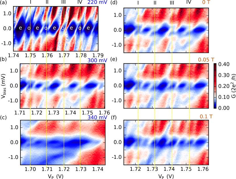
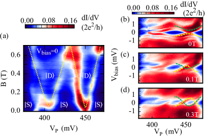
We now discuss experimental data on the singlet-doublet QPT driven by Zeeman splitting, and its relevance to the studies of Majorana bound states (MBS). We position the ’p’ and ’s’ gates in the strong coupled odd regime, where the ground state of the quantum dot is a spin-singlet at zero magnetic field (Fig. 5(a),(b)). Previous studies have shown that upon applying magnetic field a singlet-to-doublet QPT occurs. It is is marked by zero-bias peaks that appear when magnetic field shifts ABS to the middle of the gap Lee et al. (2014). At the same time, zero-bias peaks are studied as signatures of MBS which accompany a topological QPT. The topologically superconducting regime with MBS in infinite 1D nanowires is predicted for , where is the Zeeman energy, is the chemical potential that corresponds to a gate voltage Lutchyn et al. (2010); Oreg et al. (2010). The topological region within corresponds to an odd number of one-dimensional subbands crossing the Fermi level.
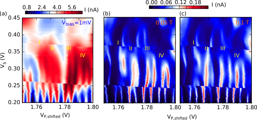
In Fig. 5(a) we show that the singlet-doublet QPC maps out a similar phase boundary to that expected for topological superconductivity. The data in Fig. 5(a) are obtained at zero bias, thus contours of high current correspond to zero-bias peaks. The ground states of the quantum dot are marked with for singlet and for doublet. Indeed we observe that the boundary between and regions has a shape similar to the topological phase boundary. Figures 5(b)-(d) show the magnetic-field driven singlet-doublet QPT from anticrossing-like to loop-like resonances extended in the source-drain bias dimension.
One key difference between the topological phase of an infinite nanowire and the magnetically-driven singlet-doublet QPT is that conductance inside the region is low because the ABS resonances have shifted away from zero bias there, as indicated in Fig. 5(d) where zero-bias peaks are strictly transient. In contrast, MBS resonances should remain at or near zero bias over an area in gate-vs-field map enclosed by the yellow dash-dot trace in Fig. 5(a). Note that here the magnetic field is applied at 30 degrees with respect to the nanowire, so no MBS are expected because the field has a significant component parallel to the spin-orbit field. However, since a small quantum dot is explicitly defined here by gates, we do not expect MBS to appear. We furthermore remark that the zero-bias conductance is not precisely zero due to resonance broadening and soft gap. Nevertheless, Fig. 5(a) adds to the list of known experimental similarities between ABS and MBS.
Acknowledgements. We thank D. Pekker, P. Yu, A. Zarassi for discussions. S.M.F. is supported by NSF DMR-1743972, NSF PIRE-1743717, ONR and ARO. R.Ž. acknowledges support from the Slovenian Research Agency (ARRS) under Grants No. P1-0044 and J1-7259.
References
- Das Sarma et al. (2015) S. Das Sarma, M. Freedman, and C. Nayak, npj Quantum Information 1, 15001 (2015).
- Tuominen et al. (1992) M. T. Tuominen, J. M. Hergenrother, T. S. Tighe, and M. Tinkham, Phys. Rev. Lett. 69, 1997 (1992).
- Eiles et al. (1993) T. M. Eiles, J. M. Martinis, and M. H. Devoret, Phys. Rev. Lett. 70, 1862 (1993).
- Lafarge et al. (1993) P. Lafarge, P. Joyez, D. Esteve, C. Urbina, and M. H. Devoret, Phys. Rev. Lett. 70, 994 (1993).
- Albrecht et al. (2016) S. M. Albrecht, A. P. Higginbotham, M. Madsen, F. Kuemmeth, T. S. Jespersen, J. Nygård, P. Krogstrup, and C. M. Marcus, Nature 531, 206 (2016).
- Janvier et al. (2015) C. Janvier, L. Tosi, L. Bretheau, Ç. Girit, M. Stern, P. Bertet, P. Joyez, D. Vion, D. Esteve, M. Goffman, et al., Science 349, 1199 (2015).
- Hays et al. (2018) M. Hays, G. de Lange, K. Serniak, D. J. van Woerkom, D. Bouman, P. Krogstrup, J. Nygård, A. Geresdi, and M. H. Devoret, Phys. Rev. Lett. 121, 047001 (2018).
- Matsuura (1977) T. Matsuura, Prog. Theor. Phys. 57, 1823 (1977).
- Satori et al. (1992) K. Satori, H. Shiba, O. Sakai, and Y. Shimizu, J. Phys. Soc. Japan 61, 3239 (1992).
- Yoshioka and Ohashi (2000) T. Yoshioka and Y. Ohashi, J. Phys. Soc. Japan 69, 1812 (2000).
- Choi et al. (2004) M.-S. Choi, M. Lee, K. Kang, and W. Belzig, Phys. Rev. B 70, 020502 (2004).
- Oguri and Tanaka (2004) A. Oguri and Y. Tanaka, Journal of the Physical Society of Japan 73, 2494 (2004).
- Bauer et al. (2007) J. Bauer, A. Oguri, and A. C. Hewson, J. Phys.: Condens. Matter 19, 486211 (2007).
- Karrasch et al. (2008) C. Karrasch, A. Oguri, and V. Meden, Phys. Rev. B 77, 024517 (2008).
- Eichler et al. (2007) A. Eichler, M. Weiss, S. Oberholzer, C. Schönenberger, A. Levy Yeyati, J. C. Cuevas, and A. Martín-Rodero, Phys. Rev. Lett. 99, 126602 (2007).
- Sand-Jespersen et al. (2007) T. Sand-Jespersen, J. Paaske, B. M. Andersen, K. Grove-Rasmussen, H. I. Jørgensen, M. Aagesen, C. B. Sørensen, P. E. Lindelof, K. Flensberg, and J. Nygård, Phys. Rev. Lett. 99, 126603 (2007).
- Buizert et al. (2007) C. Buizert, A. Oiwa, K. Shibata, K. Hirakawa, and S. Tarucha, Phys. Rev. Lett. 99, 136806 (2007).
- Grove-Rasmussen et al. (2009) K. Grove-Rasmussen, H. I. Jørgensen, B. M. Andersen, J. Paaske, T. S. Jespersen, J. Nygård, K. Flensberg, and P. E. Lindelof, Phys. Rev. B 79, 134518 (2009).
- Deacon et al. (2010) R. S. Deacon, Y. Tanaka, A. Oiwa, R. Sakano, K. Yoshida, K. Shibata, K. Hirakawa, and S. Tarucha, Phys. Rev. Lett. 104, 076805 (2010).
- Kanai et al. (2010) Y. Kanai, R. S. Deacon, A. Oiwa, K. Yoshida, K. Shibata, K. Hirakawa, and S. Tarucha, Phys. Rev. B 82, 054512 (2010).
- Pillet et al. (2010) J.-D. Pillet, C. H. L. Quay, P. Morfin, C. Bena, A. Levy Yeyati, and P. Joyez, Nature Phys. 6, 965 (2010).
- Maurand et al. (2012) R. Maurand, T. Meng, E. Bonet, S. Florens, L. Marty, and W. Wernsdorfer, Phys. Rev. X 2, 011009 (2012).
- Chang et al. (2013) W. Chang, V. E. Manucharyan, T. S. Jespersen, J. Nygård, and C. M. Marcus, Phys. Rev. Lett. 110, 217005 (2013).
- Kumar et al. (2014) A. Kumar, M. Gaim, D. Steininger, A. L. Yeyati, A. Martín-Rodero, A. K. Hüttel, and C. Strunk, Phys. Rev. B 89, 075428 (2014).
- Lee et al. (2014) E. J. H. Lee, X. Jiang, M. Houzet, R. Aguado, C. M. Lieber, and S. De Franceschi, Nature nanotechnology 9, 79 (2014).
- Jellinggaard et al. (2016) A. Jellinggaard, K. Grove-Rasmussen, M. H. Madsen, and J. Nygård, Phys. Rev. B 94, 064520 (2016).
- Lee et al. (2017) E. J. H. Lee, X. Jiang, R. Žitko, R. Aguado, C. M. Lieber, and S. De Franceschi, Phys. Rev. B 95, 180502 (2017).
- Su et al. (2017) Z. Su, A. B. Tacla, M. Hocevar, D. Car, S. R. Plissard, E. P. A. M. Bakkers, A. J. Daley, D. Pekker, and S. M. Frolov, Nature Communications 8, 585 (2017).
- Su et al. (2018) Z. Su, A. Zarassi, J.-F. Hsu, P. San-Jose, E. Prada, R. Aguado, E. J. H. Lee, S. Gazibegovic, R. L. M. Op het Veld, D. Car, S. R. Plissard, M. Hocevar, M. Pendharkar, J. S. Lee, J. A. Logan, C. J. Palmstrøm, E. P. A. M. Bakkers, and S. M. Frolov, Phys. Rev. Lett. 121, 127705 (2018).
- (30) G. A. Steele, G. Götz, and L. P. Kouwenhoven, unpublished .
- Martín-Rodero and Levy Yeyati (2011) A. Martín-Rodero and A. Levy Yeyati, Advances in Physics 60, 899 (2011).
- Luitz et al. (2012) D. J. Luitz, F. F. Assaad, T. Novotný, C. Karrasch, and V. Meden, Physical Review Letters 108, 227001 (2012).
- Meden (2018) V. Meden, “The Anderson-Josephson quantum dot – a theory perspective,” arxiv:1810.02181 (2018).
- Wilson (1975) K. G. Wilson, Rev. Mod. Phys. 47, 773 (1975).
- Bulla et al. (2008) R. Bulla, T. Costi, and T. Pruschke, Rev. Mod. Phys. 80, 395 (2008).
- Pillet et al. (2013) J.-D. Pillet, P. Joyez, R. Žitko, and M. F. Goffman, Phys. Rev. B 88, 045101 (2013).
- Žitko (2009) R. Žitko, Comp. Phys. Comm. 180, 1271 (2009).
- Jin-Guo Liu (2016) Q.-H. W. Jin-Guo Liu, Da Wang, Phys. Rev. B 93, 035102 (2016).
- Lutchyn et al. (2010) R. M. Lutchyn, J. D. Sau, and S. Das Sarma, Physical review letters 105, 077001 (2010).
- Oreg et al. (2010) Y. Oreg, G. Refael, and F. von Oppen, Physical review letters 105, 177002 (2010).
I SUPPLEMENTAL MATERIALS