Alignment-free cryogenic optical coupling to an optomechanical crystal
Abstract
The need for highly accurate, labor-intensive optical alignment has been a major hurdle in our ability to leverage the power of complex photonic integrated circuits. There is a strong need for tolerant and passive alignment methods that enable interrogation at any point in a photonic circuit. Various promising and scalable photonic packaging techniques have been under development, but few methods compatible with low-temperature operation have been reported. Here, we demonstrate alignment-free coupling efficiency from an optical fiber to a silicon optomechanical crystal at 7 mK in a dilution refrigerator. Our coupling scheme uses angle-polished fibers glued to the surface of the chip. The technique paves the way for scalable integration of optical technologies at low temperatures, circumventing the need for optical alignment in a highly constrained cryogenic environment. The technique is broadly applicable to studies of low-temperature optical physics and to emerging quantum photonic technologies.
I Introduction
The rise of integrated optical systems has motivated the development of numerous approaches to efficiently couple light from a fiber’s diameter optical mode into sub-micron confined channels on the surface of a chipVermeulen and Poulton (2018). The emerging application space of quantum sensors, computers, and communication systems necessitates its own new classes of integrated optical devices for quantum communications and control. A key challenge is to efficiently couple light in and out of these devices. Since quantum systems often have components that operate at extremely low temperatures, optical systems operating at these temperatures require coupling schemes that are both scalable and immune to the thermal stresses induced by thermal cycling. In this work, we demonstrate an approach to coupling light in and out of a silicon photonic chip at millikelvin temperatures that is robust, requires no in-situ alignment and is compatible with numerous quantum technologiesSchoelkopf and Girvin (2008); Sipahigil et al. (2016); Gould et al. (2016); Schröder et al. (2016); Witmer et al. (2017).
Common methods to address the optical input/output barrier include inverted edge tapers, evanescent couplers, and grating couplersVermeulen and Poulton (2018); Benedikovic et al. (2014); Kopp et al. (2011). Tapered fiber coupling, where a tapered fiber evanescently couples to an on-chip waveguide, has been used to achieve broadband efficient coupling at both room and cryogenic temperaturesSrinivasan and Painter (2007); Gröblacher et al. (2013); Macdonald et al. (2015). The technique uses specially formed fiber tapers and requires in-situ alignment at cryogenic temperatures, which limits the number of input-output channels and drastically increases the cost and complexity of the apparatus. Moreover, at low temperatures and in vacuum, the technique is subject to vibrational noise and power-dependent instabilities. Edge coupling has been demonstrated at cryogenic temperatures Patel et al. (2018); Meenehan et al. (2014); Riedinger et al. (2018) but also requires in-situ alignment.
Another common coupling technique utilizes gratings patterned on the surface of a chip. Well-designed grating couplers can in principle convert over of incoming light into a waveguide on the chip over a bandwidth of several THz with reflections below and using a footprint of merely tens of square micronsTaillaert et al. (2006); Benedikovic et al. (2014); Vermeulen and Poulton (2018); Notaros et al. (2016); Son et al. (2018); Michaels and Yablonovitch (2018). They allow for optical access to any point on a wafer while requiring only micron-level alignment accuracy, drastically reducing the resources necessary to interrogate complex optical circuitry. Moreover the relatively high tolerance to misalignment makes grating couplers a promising candidate for cryogenic coupling where thermal stresses increase the likelihood of the fiber moving with respect to the grating coupler. As an example of this, Shainline et al.Shainline et al. (2017) recently demonstrated a technique in which an optical fiber can be aligned to a grating coupler with the assistance of an SU-8 collar, and achieved coupling efficiencies of 21% at a temperature of without requiring low-temperature re-alignment.
Light emitted from a grating coupler is often mode-matched to SMF-28 fiber so that a cleaved fiber facet can be used to efficiently collect the radiation. The fiber, or fiber assembly, must be held at design-determined angle to the normal of the chip surface for efficient coupling. In the work by Shainline et al.Shainline et al. (2017), this was accomplished by extra layers of processing to build a supporting structure on the surface for the fiber, and a larger assembly around the chip to hold the fiber at an angle. The extra processing steps make that approach difficult to combine with released optomechanical structures. An alternative approach is to use angle-polished fibersSnyder and O’Brien (2013); Li et al. (2014) that can rest horizontally on the chip surface, obviating the need to support a fiber at an angle and leaving space for electrical connections. Total internal reflection occurring at the fiber/air interface sends light into an on-chip grating coupler at the correct angle for efficient coupling (see Figure 1a).
Here, we propose and develop a fiber-chip coupling technique, based on grating couplers and angle-polished fibers, and use it to demonstrate cryogenic measurements down to millikelvin temperatures. The technique is scalable in the sense that it provides access to many optical input and output ports on a chip at cryogenic temperatures without requiring a corresponding number of stages and control wires for preserving alignment. We demonstrate the technique by measuring a silicon optomechanical crystal in a dilution refrigerator at . The technique has good yield and the packaged devices remain stable over many cooling cycles. It circumvents the need for time-consuming manual alignment in a constrained cryogenic environment and paves the way for complex circuits with many inputs and outputs operating at low temperatures for integrated quantum optical Silverstone et al. (2016); Rudolph (2017), optomechanical Van Laer et al. (2015); Kittlaus, Shin, and Rakich (2016); Patel et al. (2017, 2018); Safavi-Naeini et al. (2019), and electro-optic Bochmann et al. (2013); Witmer et al. (2017); Van Laer et al. (2018) devices.
II Procedure
II.1 Device Fabrication
We fabricate gratings couplers attached to optomechanical crystals using a two-step silicon-on-insulator (SOI) process. First, we pattern fine features in silicon by ebeam lithography and a Cl2-based etch Patel et al. (2017, 2018). Second, we selectively suspend the optomechanical crystals but not the grating couplers by optical lithography and a buffered HF etch Van Laer et al. (2015); Van Laer (2016). We fabricate an array of such devices with a parameter sweep in the overall scaling. This allows us to frequency match the optical cavity resonance with the grating coupler response. An image of a device array is shown in Figure 1, along with an image of the fiber-coupled device.
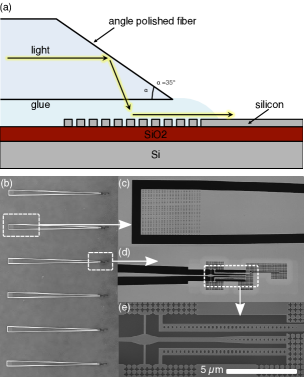
The grating coupler consists of a square array of rectangular holes fully etched into the 220 nm silicon slab according to a metagrating design Benedikovic et al. (2014) with simulated efficiencies up to . It has an impedance-matching set of smaller holes to reduce reflections off the grating (Figure 1(c)).
II.2 Fiber Gluing Procedure
To couple light into the on-chip grating couplers, we use angle-polished SMF-28 fibers (Chuxing Optical Fiber Application Technologies Ltd.) with a polish angle of approximately . The fiber is positioned horizontally above the surface of the chip. The light in the fiber experiences total internal reflection at the fiber facet and is reflected down through the bottom of the fiber, impinging on the chip surface with an angle of approximately from normal when no glue is present. This angle was chosen to recycle light reflected off the handle silicon Benedikovic et al. (2014). The coupling scheme is illustrated in Figure 1(a).
To prepare for fiber gluing, we first fasten the chip to a custom-made copper printed circuit board (PCB) using a GE Varnish/ethanol mixture. The PCB is then mounted in our fiber gluing setup, shown in Figure 2(a).
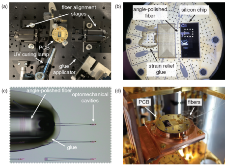
We align the angle-polished fiber to the device of interest before applying the glue. Next, we adjust the fiber X, Y, Z, yaw and roll in order to optimize the optical reflection signal from the grating coupler. We have also used this procedure for transmission devices with multiple couplers. We then apply a small drop of glue (Norland Optical Adhesive 88) to the fiber, about 0.5 to 1 mm away from the tip of the fiber. To do this we use a spare piece of SMF-28 fiber as an applicator and control the applicator position with an XYZ micrometer stage stack. After touching down the glue-tipped applicator, we move the applicator until the glue wicks underneath the fiber and covers the grating coupler by capillary action.
After the glue is applied, we find it necessary to adjust the fiber X and Y position to reoptimize the reflected signal. After reoptimizing the position, we cure the glue using a UV curing spot lamp (DYMAX BlueWave 75). We use the lamp at full power and do 6 cures of 30 seconds each, at a distance of about 3 cm and from a few different angles.
Once the fiber is glued to the chip, we apply a second, much larger drop of glue to fasten the fiber to the PCB and provide strain relief. We make sure that this second drop covers a portion of the fiber where the fiber coating is still intact to provide strength. We cure this glue in the same way as the first drop. After curing the glue, we typically leave the chip in an air environment for about 12 hours, allowing the glue to age and achieve better adhesion before installing it in the dilution refrigerator.
Once the fiber gluing process is complete, the PCB holding the chip is installed at the mixing chamber of a Bluefors dilution refrigerator (see Figure 2(d)). The dilution fridge is fitted with a series of optical fibers that provide optical access from room temperature down to the mixing chamber.
III Experimental Results
III.1 Predicting Spectral Shifts
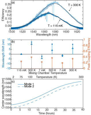
Our optical devices experience two spectral shifts during the gluing process and subsequent cooldown. First, once the glue is applied, the grating coupler spectrum undergoes a large redshift of about 91 nm (not shown). This shift stems from the refractive index of the glue ( 1.56) causing an increase in the Bloch mode index of the grating coupler. Experiments performed with oxide-clad grating couplers do not exhibit this redshift. Since the glue stays localized near the coupler, the optomechanical crystal does not undergo a frequency shift upon application of the glue. Second, both the grating coupler spectrum and the optical resonance frequency of the optomechanical crystal experience a blueshift as the chip is cooled from to millikelvin temperatures (Figure 3).
To account for these shifts, we initially measure the optical reflection spectra in air before applying any glue. We use these spectra to predict device behaviour after gluing and cooling to low temperatures. Devices of interest are selected for gluing based on their predicted behavior after the cooldown.
To understand and predict the spectral shifts quantitatively, we develop a few analytical and finite-element models. For the grating coupler, the phase-matching condition between light incoming at angle and a guided wave with wavevector is
| (1) |
with the Bloch wavevector of the guided optical mode, the free-space wavevector, the effective Bloch index, the refractive index of the medium atop the grating, which is either air () or glue () and the grating wavevector with the grating pitch. The phase-matching condition rewritten in terms of the center wavelength of the grating is
| (2) |
We are interested in perturbations of the center wavelength given perturbations in (1) the refractive index of the medium atop the grating and (2) the refractive index of the silicon. We must take into account the dispersion of the Bloch mode’s effective index to predict the size of such perturbations. Taylor-expanding the dispersion and truncating to first-order yields
| (3) |
with the group index of the Bloch mode. This expression assumes a fixed , which holds in all cases of interest here since horizontal momentum is conserved at interfaces between the fiber and the glue or air.
First, we apply equation (3) to consider the shift of the grating coupler center wavelength as we apply the glue. Our finite-element models predict a shift in the Bloch index of . This yields a predicted redshift in reasonable agreement with the observed redshift .
Second, as we cool down from to , the refractive index of silicon dropsFrey, Leviton, and Madison (2006) from to so . This perturbs the Bloch index as , leading to predicted blueshift agreeing reasonably with the observed shift of the grating coupler, (Figure 3). We neglect the temperature-dependence of the refractive index of the glue and the silicon dioxide in this calculation.
Third, we can model the optomechanical crystal as a cavity made of a waveguide supporting an optical mode with group index . The shift for such a cavity is given by
| (4) |
giving a predicted blueshift of . Finite-element modeling of the optomechanical crystal cavity optical mode confirms this: treating the refractive index shift as a perturbationChan et al. (2011); Frey, Leviton, and Madison (2006) yields in a finite-element simulation – in close agreement with the observed blueshift (Figure 3).
III.2 Optical Measurements
After gluing, the devices are mounted inside the cryostat where characterization is performed at different temperatures. We send an optical pump from a laser tuned to approximately 1550 nm to the glued angle-polished fiber. Since the device input coupling waveguide is terminated in a photonic crystal mirror whose bandwidth exceeds the grating coupler bandwidth, and whose reflection coefficient can be taken to be unity, knowledge of the external system efficiency allows us to calculate the single-pass efficiency of the grating coupler.
We summarize the observed device efficiencies over three thermal cycles in Table 1. We show the reflection spectra for one device at room temperature and at in Figure 3(a). The broad response in the reflection spectrum is due to the grating coupler, while the narrow dips are due to the optical cavity resonances. There are two such resonance per device as there are two optomechanical crystals present per coupling waveguide (Figure 1(e)). In our devices we observe optical quality factors on the order of , with no significant variation across cooldowns. An overall blueshift of the cavity wavelength and grating spectrum of approximately is observed, in excellent agreement with finite-element simulations of our structure (see above).
Occasionally a glued fiber comes loose during a cooldown and the optical reflection signal is lost outright. We believe thermal contraction of the glue is responsible for these occasional failures. The overall rate of such failures is < 25%, and if a given fiber survives its first cooldown, we find that it is highly likely to survive subsequent cooldowns. In this study device 1 failed after one thermal cycle as shown on the first row of Table 1. However, all other devices survive multiple cycles. In particular, device 3 remained intact for 10 cooldowns over the course of 6 months before being removed from the dilution fridge, without suffering substantial degradation in its optical coupling efficiency.
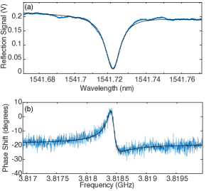
We make optomechanical measurements of the devices under continuous wave laser driving. For a device cooled to mK, we monitor the 3.8 GHz mechanical mode and measure a mechanical quality factor and a single photon optomechanical coupling rate kHz (Figure 4). For an input laser power we reach a cooperativity of – sufficient for itinerant state-transfer applications. These parameters are comparable to those used in recent heralded quantum entanglement experiments with mechanical systemsRiedinger et al. (2018).
Further improvements to our devices should allow detection efficiencies of and higher to be attainedBenedikovic et al. (2014); Notaros et al. (2016); Vermeulen and Poulton (2018); Son et al. (2018); Michaels and Yablonovitch (2018), approaching typical efficiencies in experiments using lensed fibers and adiabatic edge couplers Patel et al. (2018). One promising application of our packaging technique is the ability to simultaneously monitor multiple devices. In such schemes, the number of devices that can be probed is only limited by chip space, and the number of fiber feedthroughs on the dilution fridge. This is in contrast to using lensed fibers mounted on stages, where independent control over multiple fibers quickly becomes infeasible. Finally, it is important to note that the grating coupler must be frequency matched to the cavities of interest in any given experiment. However, this problem is readily solved by the fabrication of arrays of devices, and rapid large area testing at room temperature. Using the relations shown in this paper for wavelength shifts due to gluing and thermo-optic effects, we can deterministically predict the cavity and grating wavelength post-cooldown and select suitable devices for gluing.
| Device | T = 300 K | 116 mK | 300 K | 7 mK | 300 K | 7 mK | 300 K |
|---|---|---|---|---|---|---|---|
| 0.29 | 0.21 | 0.26 | 0.00 | 0.00 | 0.00 | 0.00 | |
| 0.36 | 0.25 | 0.40 | 0.23 | 0.37 | 0.20 | 0.34 | |
| 0.28 | 0.20 | 0.22 | 0.21 | 0.22 | 0.16 | 0.22 | |
| 0.25 | 0.20 | 0.24 | 0.19 | 0.24 | 0.21 | 0.25 |
IV Conclusion
We demonstrate alignment-free coupling with coupling efficiency from an optical fiber to a silicon optomechanical crystal at 7 mK in a dilution refrigerator. The developed angle-polished fiber gluing technique has good yield, and the packaged devices remain stable over many cooling cycles. In the future, the technique can be expanded to individually monitor many devices on a single chip in a cryogenic environment. Additionally, the gluing principle is not limited to the use of grating couplers and can be extended to other coupling schemes such as tapered fiber and edge coupling.
Acknowledgements.
This work was funded by the ARO/LPS CQTS program and NSF ECCS-1708734. Part of this work was performed at the Stanford Nano Shared Facilities (SNSF) and Stanford Nanofabrication Facility (SNF) which are supported by the National Science Foundation under award ECCS-1542152. A.S.N. acknowledges the support of a David and Lucile Packard Fellowship. R.V.L. acknowledges funding from VOCATIO and from the European Union’s Horizon 2020 research and innovation program under Marie Skłodowska-Curie grant agreement No. 665501 with the research foundation Flanders (FWO). J.D.W. acknowledges support from a Stanford Graduate Fellowship. R.N.P. is supported by a National Science Foundation Graduate Research Fellowship under grant no. DGE1656518. R.V.L. thanks Roel Baets and Dries Van Thourhout for helpful discussions.References
- Vermeulen and Poulton (2018) D. Vermeulen and C. V. Poulton, “Optical Interfaces for Silicon Photonic Circuits,” Proceedings of the IEEE 106 (2018), 10.1109/JPROC.2018.2865725.
- Schoelkopf and Girvin (2008) R. J. Schoelkopf and S. M. Girvin, “Wiring up quantum systems,” Nature 451, 664–669 (2008).
- Sipahigil et al. (2016) A. Sipahigil, R. E. Evans, D. D. Sukachev, M. J. Burek, J. Borregaard, M. K. Bhaskar, C. T. Nguyen, J. L. Pacheco, H. A. Atikian, C. Meuwly, R. M. Camacho, F. Jelezko, E. Bielejec, H. Park, M. Lončar, and M. D. Lukin, “An integrated diamond nanophotonics platform for quantum-optical networks.” Science (New York, N.Y.) 354, 847–850 (2016).
- Gould et al. (2016) M. Gould, S. Chakravarthi, I. R. Christen, N. Thomas, S. Dadgostar, Y. Song, M. L. Lee, F. Hatami, and K.-M. C. Fu, “Large-scale GaP-on-diamond integrated photonics platform for NV center-based quantum information,” Journal of the Optical Society of America B 33, B35 (2016).
- Schröder et al. (2016) T. Schröder, S. L. Mouradian, J. Zheng, M. E. Trusheim, M. Walsh, E. H. Chen, L. Li, I. Bayn, and D. Englund, “Quantum nanophotonics in diamond [Invited],” Journal of the Optical Society of America B 33, B65 (2016).
- Witmer et al. (2017) J. D. Witmer, J. A. Valery, P. Arrangoiz-Arriola, C. J. Sarabalis, J. T. Hill, and A. H. Safavi-Naeini, “High-Q photonic resonators and electro-optic coupling using silicon-on-lithium-niobate,” Scientific Reports 7, 46313 (2017).
- Benedikovic et al. (2014) D. Benedikovic, P. Cheben, J. H. Schmid, D. X. Xu, J. Lapointe, S. Wang, R. Halir, A. Ortega-Moñux, S. Janz, and M. Dado, “High-efficiency single etch step apodized surface grating coupler using subwavelength structure,” Laser and Photonics Reviews 8, L93–L97 (2014).
- Kopp et al. (2011) C. Kopp, S. Bernabé, B. B. Bakir, J. M. Fedeli, R. Orobtchouk, F. Schrank, H. Porte, L. Zimmermann, and T. Tekin, “Silicon photonic circuits: On-CMOS integration, fiber optical coupling, and packaging,” IEEE Journal on Selected Topics in Quantum Electronics 17, 498–509 (2011).
- Srinivasan and Painter (2007) K. Srinivasan and O. Painter, “Optical fiber taper coupling and high-resolution wavelength tuning of microdisk resonators at cryogenic temperatures,” Applied Physics Letters 90, 031114 (2007).
- Gröblacher et al. (2013) S. Gröblacher, J. T. Hill, A. H. Safavi-Naeini, J. Chan, and O. Painter, “Highly efficient coupling from an optical fiber to a nanoscale silicon optomechanical cavity,” Applied Physics Letters 103, 1–4 (2013), arXiv:1309.1181 .
- Macdonald et al. (2015) A. J. R. Macdonald, G. G. Popowich, B. D. Hauer, P. H. Kim, A. Fredrick, X. Rojas, P. Doolin, and J. P. Davis, “Optical microscope and tapered fiber coupling apparatus for a dilution refrigerator,” Rev. Sci. Instrum 86, 13107 (2015).
- Patel et al. (2018) R. N. Patel, Z. Wang, W. Jiang, C. J. Sarabalis, J. T. Hill, and A. H. Safavi-Naeini, “Single-Mode Phononic Wire,” Physical Review Letters 121, 40501 (2018), arXiv:1711.00847 .
- Meenehan et al. (2014) S. M. Meenehan, J. D. Cohen, S. Gröblacher, J. T. Hill, A. H. Safavi-Naeini, M. Aspelmeyer, and O. Painter, “Silicon optomechanical crystal resonator at millikelvin temperatures,” Physical Review A 90, 011803 (2014).
- Riedinger et al. (2018) R. Riedinger, A. Wallucks, I. Marinković, C. Löschnauer, M. Aspelmeyer, S. Hong, and S. Gröblacher, “Remote quantum entanglement between two micromechanical oscillators,” Nature 556, 473–477 (2018), arXiv:1710.11147 .
- Taillaert et al. (2006) D. Taillaert, F. Van Laere, M. Ayre, W. Bogaerts, D. Van Thourhout, P. Bienstman, and R. Baets, “Grating couplers for coupling between optical fibers and nanophotonic waveguides,” Japanese Journal of Applied Physics, Part 1: Regular Papers and Short Notes and Review Papers 45, 6071–6077 (2006).
- Notaros et al. (2016) J. Notaros, F. Pavanello, M. T. Wade, C. M. Gentry, A. Atabaki, L. Alloatti, R. J. Ram, and M. A. Popović, “Ultra-Efficient CMOS Fiber-to-Chip Grating Couplers,” in Optical Fiber Communication Conference (OSA, Washington, D.C., 2016) p. M2I.5.
- Son et al. (2018) G. Son, S. Han, J. Park, K. Kwon, and K. Yu, “High-efficiency broadband light coupling between optical fibers and photonic integrated circuits,” Nanophotonics 7, 1845–1864 (2018).
- Michaels and Yablonovitch (2018) A. Michaels and E. Yablonovitch, “Inverse design of near unity efficiency perfectly vertical grating couplers,” Optics Express 26, 4766 (2018), arXiv:1705.07186 .
- Shainline et al. (2017) J. M. Shainline, S. M. Buckley, N. Nader, C. M. Gentry, K. C. Cossel, J. W. Cleary, M. Popović, N. R. Newbury, S. W. Nam, and R. P. Mirin, “Room-temperature-deposited dielectrics and superconductors for integrated photonics,” Optics Express 25, 10322 (2017).
- Snyder and O’Brien (2013) B. Snyder and P. O’Brien, “Packaging process for grating-coupled silicon photonic waveguides using angle-polished fibers,” IEEE Transactions on Components, Packaging and Manufacturing Technology 3, 954–959 (2013).
- Li et al. (2014) C. Li, K. S. Chee, J. Tao, H. Zhang, M. Yu, and G. Q. Lo, “Silicon photonics packaging with lateral fiber coupling to apodized grating coupler embedded circuit,” Optics Express 22, 24235 (2014).
- Silverstone et al. (2016) J. W. Silverstone, D. Bonneau, J. L. O’Brien, and M. G. Thompson, “Silicon Quantum Photonics,” IEEE Journal of Selected Topics in Quantum Electronics 22, 390–402 (2016).
- Rudolph (2017) T. Rudolph, “Why I am optimistic about the silicon-photonic route to quantum computing,” APL Photonics 2, 030901 (2017), arXiv:1607.08535 .
- Van Laer et al. (2015) R. Van Laer, A. Bazin, B. Kuyken, R. Baets, and D. Van Thourhout, “Net on-chip Brillouin gain based on suspended silicon nanowires,” New Journal of Physics 17, 115005 (2015), arXiv:arXiv:1508.0631 .
- Kittlaus, Shin, and Rakich (2016) E. A. Kittlaus, H. Shin, and P. T. Rakich, “Large Brillouin amplification in silicon,” Nature Photonics 10, 463–467 (2016), arXiv:1510.08495 .
- Patel et al. (2017) R. N. Patel, C. J. Sarabalis, W. Jiang, J. T. Hill, and A. H. Safavi-Naeini, “Engineering phonon leakage in nanomechanical resonators,” Physical Review Applied 041001, 1–5 (2017), arXiv:1705.07869 .
- Safavi-Naeini et al. (2019) A. H. Safavi-Naeini, D. Van Thourhout, R. Baets, and R. Van Laer, “Controlling phonons and photons at the wavelength scale: integrated photonics meets integrated phononics,” Optica 6, 213 (2019).
- Bochmann et al. (2013) J. Bochmann, A. Vainsencher, D. D. Awschalom, and A. N. Cleland, “Nanomechanical coupling between microwave and optical photons,” Nature Physics 9, 712–716 (2013).
- Van Laer et al. (2018) R. Van Laer, R. N. Patel, T. P. McKenna, J. D. Witmer, and A. H. Safavi-Naeini, “Electrical driving of X-band mechanical waves in a silicon photonic circuit,” APL Photonics 3, 086102 (2018), arXiv:1806.04100 .
- Van Laer (2016) R. Van Laer, Light-sound interaction in nanoscale silicon waveguides, Ph.D. thesis, Ghent University (2016).
- Frey, Leviton, and Madison (2006) B. J. Frey, D. B. Leviton, and T. J. Madison, “Temperature-dependent refractive index of silicon and germanium,” Optomechanical Technologies for Astronomy 6273, 62732J (2006), arXiv:0606168 [physics] .
- Chan et al. (2011) J. Chan, T. P. Alegre, A. H. Safavi-Naeini, J. T. Hill, A. Krause, S. Gröblacher, M. Aspelmeyer, and O. Painter, “Laser cooling of a nanomechanical oscillator into its quantum ground state,” Nature 478, 89–92 (2011), arXiv:1106.3614 .