, ,
Effective resistance of random percolating networks of stick nanowires : functional dependence on elementary physical parameters
Abstract
We study by means of Monte-Carlo numerical simulations the resistance of two-dimensional random percolating networks of stick, widthless nanowires. We use the multi-nodal representation (MNR) Rocha2015 to model a nanowire network as a graph. We derive numerically from this model the expression of the total resistance as a function of all meaningful parameters, geometrical and physical, over a wide range of variation for each. We justify our choice of non-dimensional variables applying Buckingham theorem. The effective resistance of 2D random percolating networks of nanowires is found to write as where , are the geometrical parameters (number of wires, aspect ratio of electrode separation over wire length) and , , are the physical parameters (nanowire linear resistance per unit length, nanowire/nanowire contact resistance, metallic electrode/nanowire contact resistance). The dependence of the resistance on the geometry of the network, one the one hand, and on the physical parameters (values of the resistances), on the other hand, is thus clearly separated thanks to this expression, much simpler than the previously reported analytical expressions.
I Introduction
The study of random percolating networks of conducting nanowires has become in the last years a hot topic of investigation. Numerous applications are possible thanks to the outstanding electrical and optical performances of such thin films, combined to their low cost and ease of fabrication. Applications are as diverse as thin film transistors based on carbon nanotubes networks (CNNs) Li2007 ; Li2008 , CNNs-based field-effect transistors Li2009 , transparent conductive (high transmittance, low resistance) thin-film electrodes based on silver nanowires Rocha2015 ; OCallaghan2016 or carbon nanotubes (CNTs) Hecht2006 – useful for instance in the context of solar cells, the conducting nanowire network acting as a charge carrier collector Kumar2017a – and sensors Li2009 .
The conductivity, as well as the sheet transmittance of such thin film nanowire networks has been extensively studied experimentally and theoretically Hecht2006 ; Nirmalraj2009 ; Forro2018 . These systems are well approximated by random 2D networks, and we study in this paper the dependence of their effective resistance on all structural and physical parameters. We focus on the functional dependence of the resistance on physical parameters, motivated by sensor applications of nanowire networks. In this context, physical parameters, such as nanowire linear resistance, or nanowire/nanowire contact resistance, can vary, due to environment changes. The geometry and structure of the network is thus not sufficient to understand properly the resistance variations.
Many parameters impact the total effective resistance of nanowire random networks. Structural parameters such as the density (or coverage), the aspect ratio of electrode separation to wire length, and the alignment of the wires (i.e. the statistical distribution of their angles with respect to a fixed direction) are, among others, known to play on the transport properties of the networks, as confirmed experimentally and numerically in Kocabas2007 .
Simoneau and al. studied numerically the influence on the estimated effective resistance of the statistical distribution chosen for angles, lengths, diameters of nanowires (in that case CNTs) Simoneau2013 , waviness, degree of penetration of CNTs Simoneau2015 , under the junction dominated assumption (JDA) – i.e. assuming ballistic transport in individual CNTs. The mean tube length, the porosity (or equivalently, the volume fraction of CNTs) and the dimension of the network (distance between the electrodes) are also crucial geometrical parameters well studied in the literature. For instance, Lyons and al. Lyons2008 used an empirical relation relating the mean tube length and the porosity of the network to the total number of junctions, which is shown to mainly drive the film conductivity. The aspect ratio of the rods themselves (i.e. length over diameter), when they are not modeled as widthless sticks, is also a possible varying parameter, whose influence on the total resistance has been studied by Mutiso and al. Mutiso2013 .
Concerning physical parameters, the influence of junction resistance (nanowire/nanowire contact resistance, denoted as in the following) on the overall resistance was reported qualitatively, from experimental measurements Hecht2006 , while a linear relationship between the conductivity and the number of junctions was established in Lyons2008 for CNTs networks. Several studies addressed the question of the influence of a change of this contact resistance between two nanowires on the overall resistance. Nimalraj and al. measured the distribution of junction resistances as a function of the diameter and treatment (acid treatment, annealing, pristine CNTs), and the influence of its variation on the total resistance of the network Nirmalraj2009 . Finally, Behnam and al. Behnam2007 studied numerically the dependence of the scaling (with respect to the width of the conducting channel) of the resistance of 2D nanowire networks, on nanotube length, nanotube alignment, and on the ratio of junction to linear resistance (still assuming ballistic transport in CNTs). The linear resistance of nanowires was fixed to the ballistic resistance value, so that its contribution to the whole resistance was not studied in the diffusive regime in Ref. Behnam2007 , nor did the authors derive a functional dependence of the effective resistance on all the parameters.
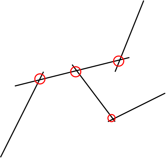
In the articles previously mentioned, the electronic transport in the percolating network is assumed dominated by the junction resistances, and the contribution of linear resistances, i.e. of the wires themselves, are neglected – Junction Dominated Assumption (JDA). Zezelj and al. performed in 2012 a pioneering study of the dependence of conductivity local critical exponents on the junction to linear resistance ratio Zezelj2012 . da Rocha and al. introduced in 2015 the Multi Nodal Representation (MNR) method Rocha2015 , generalizing the JDA – mostly used in the previous studies, e.g in Mutiso2013 –, to include wire resistances. In MNR, an electrical circuit made up of randomly dispersed nanowires is represented as a graph, with nodes at the crossing points of nanowires and edges (modelling connecting resistors) in-between. It is also the spirit of the method of nodal potentials already used in Ref. Wu2004 ; Kagan2015 , whose idea is to represent each point where the potential is well defined as a node. To account for the resistances across nanowires junctions, each node is then duplicated, yielding two nodes each representing the contact point on one nanowire Rocha2015 ; Kim2018 – every node is thus attached to a given nanowire. A new edge with junction conductance is created in-between. A typical example of construction of the graph is shown Figure 1.
da Rocha and al. applied this method to derive the contribution of both junction and linear resistances to the total resistance Rocha2015 . This allows to compute the minimal reachable network resistance. Indeed, for silver nanowires networks, the goal is often to decrease as much as possible the contribution of junction resistances. In the limit of zero junction resistances, the effective resistance is given by the contribution of linear resistances only. In 2016, O’Callaghan and al. introduced an equivalence between a random disordered network of nanowires and a regular (square) ordered network, the edges of the associated graph all having the same resistance OCallaghan2016 . They used effective medium theory arguments, introduced by Kirkpatrick Kirkpatrick1973 , valid over a certain regime (high above percolation) and exact only in the case of an infinite medium. The authors thus derived a closed-form expression for the homogeneous edge resistance of a square lattice equivalent to (i.e. having same total resistance as) the initial disordered network. Incidentally, as they used the MNR method to describe the network, this yielded an expression of the effective resistance as a function of geometrical parameters (number of wires) and physical parameters (with both linear and junction resistances), reported in Table 1. The contact resistance between the metallic electrodes and the nanowires was not included in the model. In 2018, Kim and al. used the same MNR method and a block-matrix representation of Kirchhoff’s laws to derive the effective conductivity of 2D random percolating networks of widthless rods Kim2018 , with three varying geometrical and structural parameters (aspect ratio , length of the rods , density of tubes ). However, as underlined by the authors, the internal resistance (linear resistance of the wires), although included in the model, was taken constant over all edges of the underlying graph – while it depends actually on the length of the edge in the diffusive regime. Moreover, the ratio of linear over junction resistance was fixed for the whole study. Thus, the functional dependence on the physical parameters (linear resistance per unit length of a nanowire, denoted as in the following, junction resistance , and metallic electrode/nanowire resistance, denoted as ) was not investigated.
Finally, Forró and al. Forro2018 also recently derived an analytical expression of the sheet resistance of random 2D networks of nanowires, valid at rather high densities (well above the percolation threshold), as a function of both geometrical parameters (wire density, wire length and electrode separation) and physical parameters (contact resistance) and – wire resistance, equal in our notations to where is the length of a wire – as seen in Eq. (6) of Ref. Forro2018 , reported Table 1. The authors assumed that the transport properties of the random network was the same as in an equivalent system of individual decoupled wires, with a linear average potential background. For the first time, average individual contact and linear resistance values and were extracted by fitting experimental values of resistances of SWCNTs thin films, of varying geometrical parameters, with and among the fitting parameters. This is worth mentioning as, except thanks to AFM measurements, the individual junction resistances and the average linear resistance cannot be deduced from the measured total resistance of a network. Still, the analytical expression of the total resistance derived by Forro and al. does not allow to separate the contributions of all linear resistances and of all the contact resistances to the total resistance (e.g. as a sum), contrary to the work of da Rocha and al. Rocha2015 . Moreover, electrode/nanowire resistance was not treated as an independent variable in this study Forro2018 , but taken proportional to the nanowire/nanowire contact resistance .
| Reference | Variables considered | Formula | Method | Validity of the expression and drawbacks |
| Forró and al. Forro2018 | , , , , (see expression in Forro2018 ) | Equivalent system of decoupled wires with linear average potential background | High density | |
| O’Callaghan and al. OCallaghan2016 | , , , average segment length , wire length , device size | , the expressions of , and are given below | Effective medium theory Kirkpatrick1973 | High above percolation, infinite medium. Assumption of small-world network behavior. |
| Kim and al. Kim2018 | Aspect ratio , length of the rods , density | No analytical expression | Block-matrix representation of Kirchoff’s laws | Ballistic internal wire resistance , fixed ratio (linear to junction resistance) |
| Zezelj and al. Zezelj2012 | Stick conductance , junction conductance , density , aspect ratio | Empirical expression (understanding and validation in terms of critical exponents) | Expression of this form in and on the whole density range (with modified geometrical coefficients to include finite-size effects on some ranges). |
where and , , a constant
The main recent results concerning the functional dependence of the effective resistance of 2D random nanowire networks on physical (and geometrical) parameters – i.e. individual resistances of the components – are summarized Table 1. We notice that very different expressions of the effective resistance as a function of the physical parameters have been reported, depending on the particular approach used. Moreover, the contact resistance between metallic electrodes and nanowires has never been included in these models.
We propose in this paper a different approach to derive an approximate analytical expression of the effective resistance of a random percolating network of nanowires, neither based on percolation nor on effective medium approaches. We study the dependence on all relevant geometrical and physical parameters, for a given random network generating procedure. We also use the MNR method to describe the percolating network of nanowires, including both linear and contact resistances ( and ) as in Ref. Rocha2015 ; OCallaghan2016 ; Kim2018 , and adding the electrode/nanowire contact resistance in the model, for the first time. A closed form expression for the effective resistance, as a function of these physical parameters, is estimated numerically, by means of Monte-Carlo simulations and fitting of the obtained data points. The effective resistance is found to write as simply as , validating numerically (in the particular case of ) the empirical functional dependence on the linear and junction resistances proposed by Zezelj and al. Zezelj2012 .
II Method
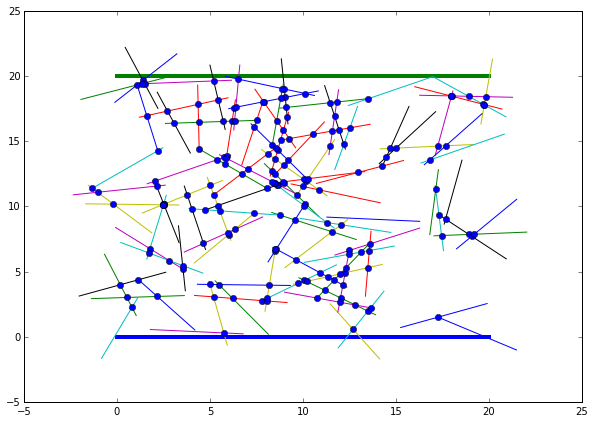
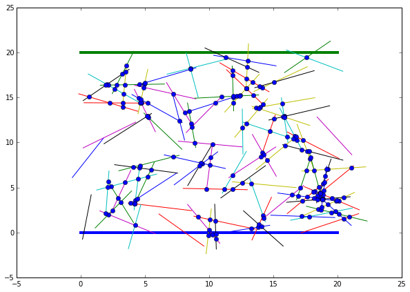
Two-dimensional random percolating networks of nanowires are generated by chosing randomly the positions of the centers of wires in the rectangle representing the device surface ( being the length of the channel and the width of the electrodes) and their angles with respect to the direction of the two electrodes (represented by the segment lines and ), following a uniform law in both cases. All the wires are assumed to have the same length . All the positions of the contacts between two wires are found analytically (as the wires are assumed widthless) and associated to ”internal” nodes of an underlying graph. The contacts which are on top of one of the electrodes are discarded as the current will flow preferentially from the metallic electrode to the nearest contact inside the device. Two examples of generated networks are depicted on Figure 2, with the detailed contributions of each type of resistance to the effective resistance (see section III). An example of construction of the underlying graph around 4 contacts is illustrated on Figure 1. The ”internal” nodes are first linked by edges of distance dependent resistance ( where is the wire resistance per unit length and the distance between two contacts indexed and ). The transport in individual wires is thus considered diffusive. Each of these nodes is then duplicated, and edges associated to contact resistances are added between each new pair of duplicated nodes. Finally, two other ”external” nodes are added to account for the two electrodes, and linked to nearest contacts along the wires contacting them (with an edge associated to a resistance , where is the contact resistance between the metallic electrode and the wire, being the shortest distance between the electrode and the first contact along the wire). From the construction of the graph detailed above, , the total number of nodes, is of order twice the number of contacts between nanowires.
The conductance matrix associated to this underlying graph is built accordingly, and allows to express Kirchhoff’s laws, written at all the nodes, in a matrix form. We define the vector of all the (algebraic) currents leaving the nodes :
| (1) |
which accounts for the injected current at the lower electrode (labeled by index ), flowing out at the higher electrode (labeled by index ). At all the other ”internal” nodes, the current entering the node is equal to the current leaving the node. The entries of the vector are the potentials at all the nodes of the graph (including the two nodes corresponding to the two electrodes) :
| (2) |
and are related one to another by the conductance matrix :
| (3) |
Equation 3 simply corresponds to the Kirchhoff laws written at each node. The (symmetric positive) matrix in equation 3 is given by :
| (4) |
where is equal either to (edge of linear resistance), (edge of contact resistance), or (edge between the metallic electrode and an internal node). We choose the same contact resistance to model all the junctions on the network (all the edges associated to contact resistances have thus the same conductance ), while the edges of nanowire linear pathways have a resistance proportional to the distance (contrary to the model of Ref. Kim2018 ), i.e. the transport in nanowires is assumed to be diffusive. It would be also possible to handle probabilistic distributions of contact and linear resistances.
In our model, each node is connected to a contact resistance edge, and one or two wire segments (one only in the case of a dead-end attached wire segment). Dead-end wire segments are not represented in the graph as they do not participate to the conduction. The degree of the nodes of the graph is thus either two or three for all inner nodes. The two nodes representing the two electrodes have a much higher connectivity, corresponding to the number of pathway departures or endings.
Non-dimensionalization of the problem :
We assume that the device is large enough so that the effective resistance has ohmic behavior, i.e. is inversely proportional to the device width. Thus, we can choose a square device area () without loss of generality. The effective resistance depends thus a priori on six independent physical variables , , , , and , so that there is a function satisfying . Performing a dimensional analysis and applying Buckingham theorem leads to five independent non-dimensional variables only, which can be for instance taken as – see Appendix for details. We can thus write the complete dependence of the non-dimensional effective resistance on both physical non-dimensional parameters and and geometrical parameters as :
| (5) |
In order to obtain explicitly this form, we rewrite a non-dimensionalized version of equation 3 :
| (6) |
where is a reference current, a reference potential, and a reference resistance. and are the non-dimensionnalized vectors of all node potentials and of all current leaving the nodes. The conductance matrix has coefficients of the following form, only :
| (7) |
where and are the set of indexes of nodes linked to the lower and outer electrode respectively. We choose , the length of a wire, as a reference distance and , the contact resistance, as normalizing resistance. can be rewritten as a matrix with non-dimensional entries :
| (8) |
Let us introduce the non-dimensional parameters and . We therefore have rewritten the conductance matrix as :
| (9) |
The ratios are geometrical features, and depend on the morphology of the randomly generated network only – they are thus constant for a given fixed network. The ratio of wire linear resistance to wire/wire contact resistance , plays as a parameter in the matrix, and so does the ratio of the contact resistance between electrode and nanowire to the junction resistance. Their values control the conduction regime, for instance dominated by contact resistance if .
Solving the resistor network problem formulated as is elementary for networks of moderate size. Several methods are possible to solve Kirchhoff laws, e.g. thanks to iterative solvers Zezelj2012 ; Simoneau2013 ; Simoneau2015 . The details of the calculation methods are reported in Appendix . The true resistance, expressed as a function of the physical parameters, is therefore :
| (10) |
where is the non-dimensional effective resistance, in units of , computed from the non-dimensional conductance matrix . Non-dimensionalizing the problem has enabled us to reduce a problem dependent on three physical variables (, and ) to a problem function of two variables ( and ) only. The dependence of the resistance on the random network generating process, on its structure and geometry (number of wires or normalized density , dimensions of the device area) is implicit through the geometrical (random) factors factoring and in the matrix and via the size of the matrix . This matrix dimension is of order twice the number of contacts. The latter depends directly on the number of wires and on the aspect ratio (from Ref. Heitz2011 , it can be estimated as ).
In the following, we perform numerical simulations to estimate an analytical expression of , focusing on the functional dependence on physical parameters and – the associated geometrical factors being the results of fitting and averages.
III Results
The functional dependence of the effective resistance on the physical parameters (, , , i.e. and in terms on non-dimensional parameters) has been first investigated for fixed percolating networks of nanowires, at a given aspect ratio . Then, for the sake of generality and applicability of the model to real devices – of random, unpredictable geometry –, this functional dependence on the resistance of the individual components of the network (, , ) was generalized for average networks by averaging, at a given aspect ratio , over several realizations of random networks made up of nanowires.
At fixed random network :
Fixing a percolating network allows one to fix the geometry and to have the physical parameters (resistances) vary, through the variation of and , without the variability due to the randomness of the network construction. For a given fixed network, the effective non-dimensional resistance obtained by solving the linear system is in the most general case a rational fraction of and (see Appendix for the details of the calculations).
Here, we show numerically that can be reduced to a very good level of accuracy, for any fixed network of nanowires above percolation, to a simple sum a linear terms in and , plus a constant : (over the physically relevant ranges of values of and ). This formula appears to be a very good approximation at any density above the percolation level.
First, a random network of nanowires is generated and its associated conductance matrix computed. The effective resistance is computed for values of such that the ratio varies over the range 0.01 to 1 (with steps of ) and such that varies over the range 0.1 to 1 (with steps of ), i.e. for a total of 1000 different values of . This enables to span all the conduction regimes – from junction resistances dominated to linear resistance dominated, for instance. The function is then fitted to the obtained data points by linear regression. The geometrical parameters are thus fixed.
This procedure can be repeated for different values of and – fixing a given generated network, for each value of . We obtain the following form, from least-squares fitting of to the computed data points, at each fixed geometry :
| (11) |
The result 11 is found to be valid for any network above the percolation threshold (with varying approximation errors on parameters , and depending on the geometry and the distance with respect to percolation). Examples of coefficients , and , for fixed nanowire networks of different densities (for a same device aspect ratio ), are given table 2, as well as fitting errors. It can be seen from the results displayed in table 2 that equation 11 holds to a very high degree of accuracy, given the very low standard deviations on the fitted geometrical parameters , and .
In physical units, from equation 11, the true resistance of a fixed given network is :
| (12) |
This decomposition of the effective resistance into its three different contributions (of different physical origin) is given for the random networks of Figure 2. The coefficients , and are purely geometrical factors. They could be interpreted as the ratio of the mean number of linear portions (or respectively of nanowire/nanowire junctions, or electrode/nanowire contacts) per ”typical” percolation pathway, to the number of such typical pathways (in a picture of parallel identical pathways). A very simple interpretation can also be a model with three resistances in series, each one accounting for the contributions of all the resistances of the network of a certain kind (linear, wire/wire junction, or electrode/wire contact), rescaled by a geometrical factor dependent on the number of wires and aspect ratio only.
| Number of nanowires | Distance to percolation | ||||||
| 150 | 1.66 | 0.818 | 2.00 10-4 | 1.153 | 1.00 10-3 | 0.195 | 1.20 10-3 |
| 200 | 2.22 | 0.435 | 2.00 10-4 | 0.482 | 7.00 10-4 | 0.196 | 8.00 10-4 |
| 250 | 2.77 | 0.267 | 1.00 10-4 | 0.260 | 4.00 10-4 | 0.118 | 5.00 10-4 |
| 300 | 3.33 | 0.178 | 7.00 10-5 | 0.145 | 3.00 10-4 | 8.21 10-2 | 4.00 10-4 |
| 350 | 3.88 | 0.149 | 6.00 10-5 | 0.101 | 3.00 10-4 | 8.28 10-2 | 3.00 10-4 |
| 400 | 4.43 | 0.126 | 5.00 10-5 | 8.27 10-2 | 2.00 10-4 | 5.73 10-2 | 3.00 10-4 |
| 450 | 4.99 | 0.116 | 5.00 10-5 | 6.81 10-2 | 2.00 10-4 | 7.19 10-2 | 2.00 10-4 |
Averaging over random networks :
Real random percolating networks of nanowires do not have a predictable geometry. Rather, they can be viewed as representatives of the class of all possible random percolating networks of nanowires at a given density (which is known or at least estimated experimentally). The detailed structure (i.e. the positions of all the wires, angles, and positions of the contacts) of a real random network of nanowires – of given density – is difficult to characterize from imaging techniques, specially at very high density, well above the percolation threshold. Capturing the actual precise distribution of wires from an SEM analysis of a real network was nonetheless done in Ref. Rocha2015 , for very low density networks of silver nanowires. As the reproducibility of the resistance of a given network increases with its density, for high density networks, a good estimation of the geometrical factors , and governing the effective resistance would be given by the coefficients averages over some realizations of random networks of same density.
For this purpose, we averaged, for each value of the physical variables , the computed values of resistances for several random networks made up of nanowires (with fixed). We obtained, after fitting, the same functional dependence (on physical parameters) for the average effective resistance of random percolating networks made up of nanowires (at a fixed geometry ), this time with average coefficients :
| (13) |
in terms of non-dimensional effective resistance and :
| (14) |
in physical units.
Let be the set of possible realizations of random networks of nanowires (with a geometry characterized by the aspect ratio ) and denote a particular realization. Expression 13 amounts to approximate, at each fixed value of and fixed values of and , the effective resistance (seen as a random variable from to ) by its average . The effective resistance of random networks of nanowires, all parameters being fixed, is indeed a well-behaved unimodal random variable, which can be fairly well approximated by its average value and standard deviation. We justified this assumption by calculating probability distributions of the network effective resistance, all parameters (geometrical and physical) being fixed. It yielded a trend depicted on Figure 3 – which had already been reported in the context of small-world resistor networks Korniss2006 .
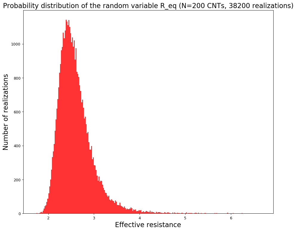
Varying the number of nanowires and the aspect ratio only changes the mean resistance and the standard deviation but does not change the shape of this law. Incidentally, this law gives an indication of the experimental non-reproducibility of the resistance that has to be expected when fabricating random nanowire networks.
The expression :
| (15) |
at is reminiscent of the empirical expression of Zezelj and al. Zezelj2012 successfully introduced to explain the high-density behavior of the local conductivity exponent depending on the junction resistance to wire resistance ratio (no electrode/wire contact resistance was included). The geometrical factors proposed in Ref. Zezelj2012 are and , for dense networks, well above percolation, and at fixed aspect ratio .
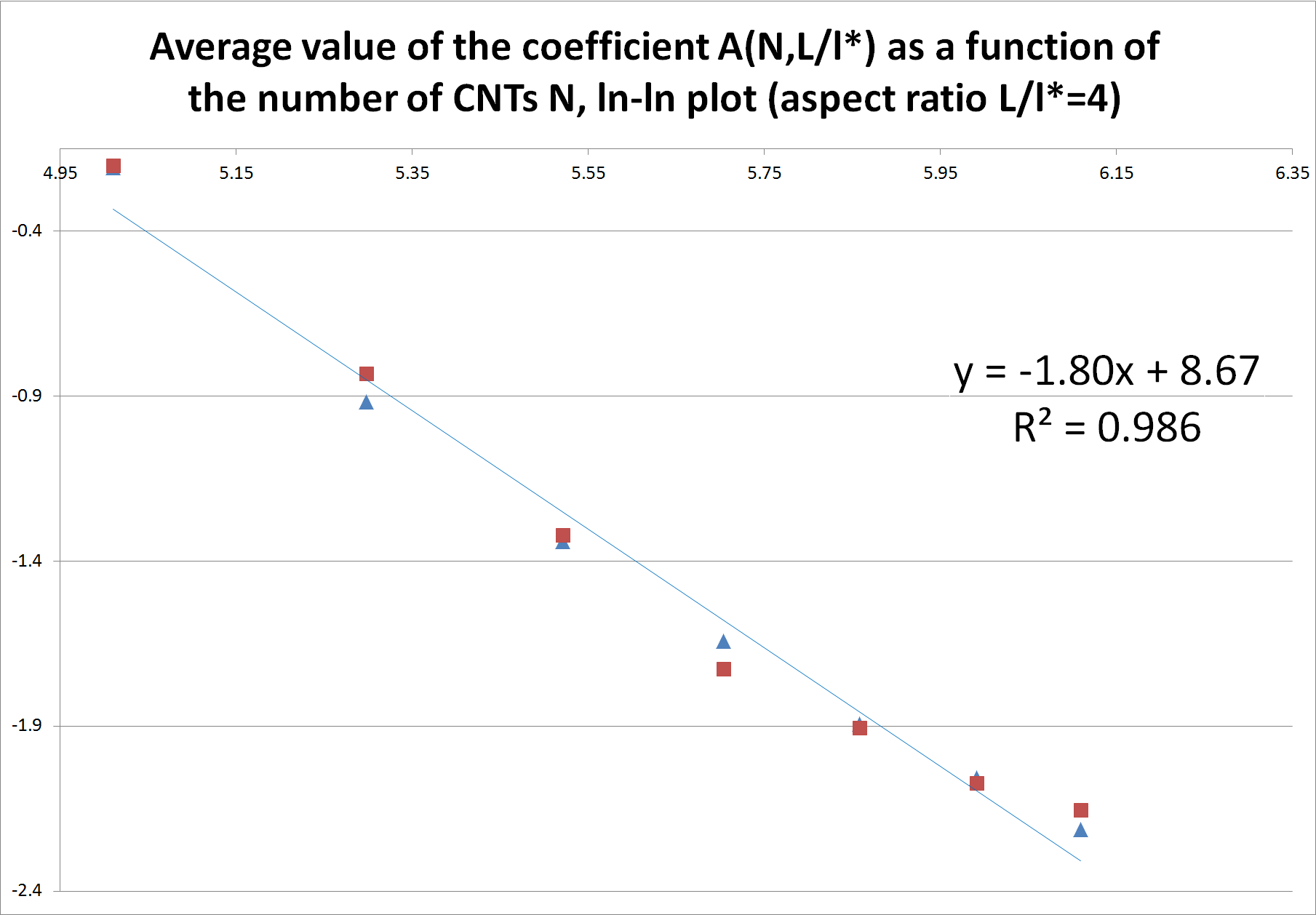
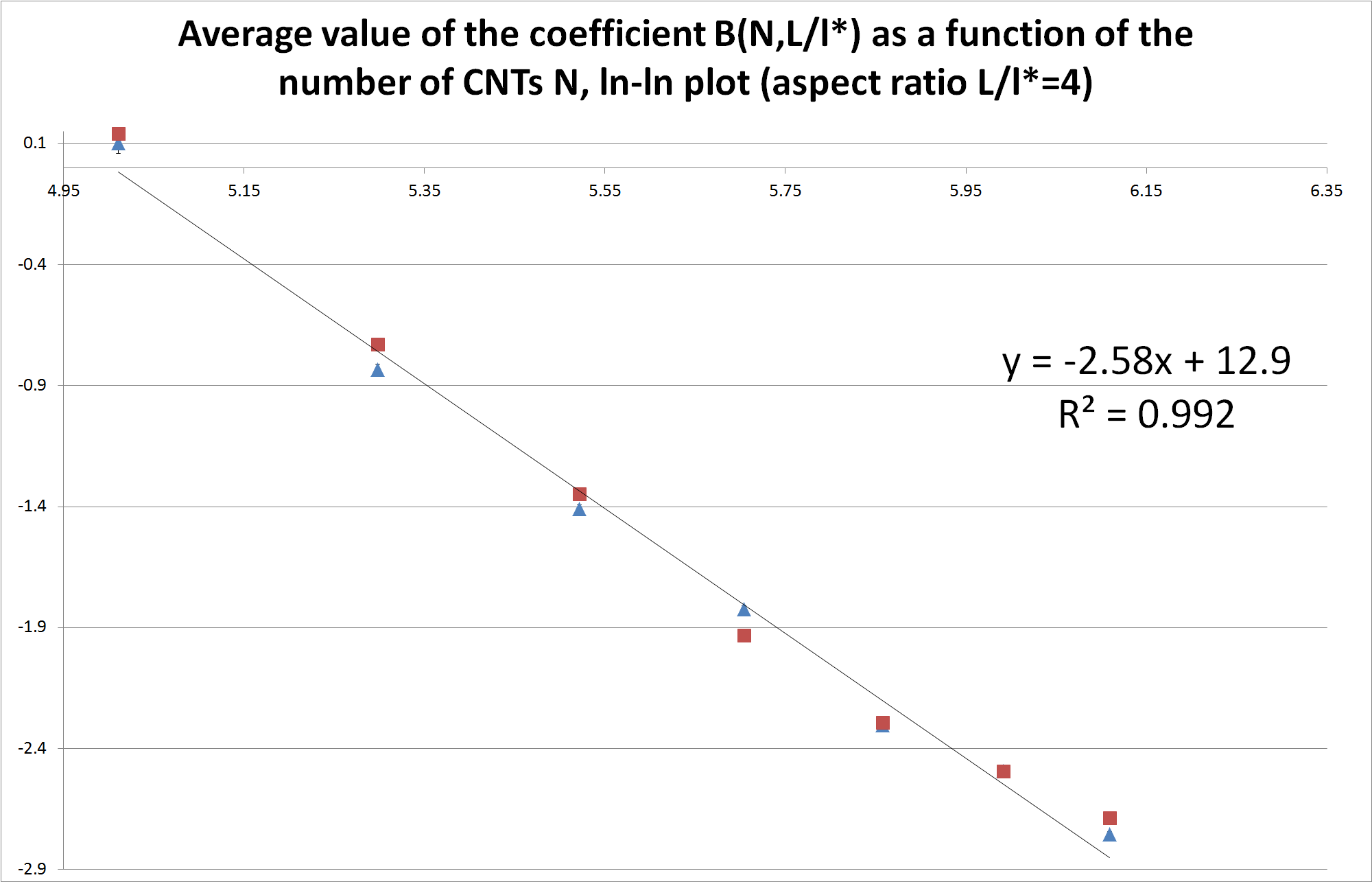
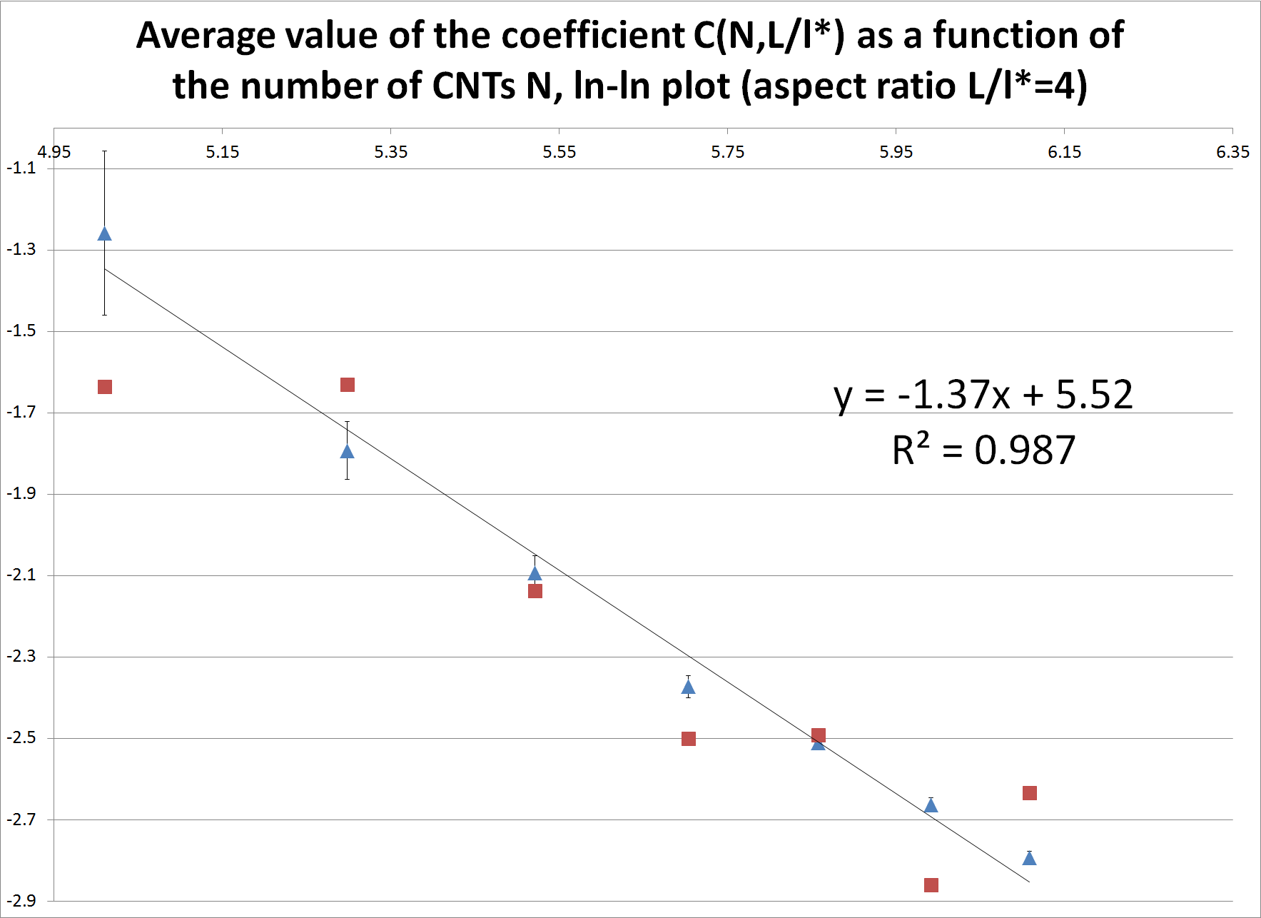
The values found for the average coefficients , and for an aspect ratio are reported table 3 as a function of the number of wires , and plotted on Figure 4. These three geometrical coefficients decrease with increasing number of wires following a power-law dependence, typical of percolation : , and with critical exponents , and . We note that these exponents are different from those of Ref. Zezelj2012 .
| Number of nanowires (N) | Distance to percolation | ||||||
| 150 | 1.66 | 0.812 | 1.14 10-2 | 1.11 | 4.58 10-2 | 0.284 | 5.74 10-2 |
| 200 | 2.22 | 0.400 | 2.30 10-3 | 0.435 | 9.40 10-3 | 0.167 | 1.18 10-2 |
| 250 | 2.77 | 0.262 | 1.00 10-3 | 0.245 | 4.10 10-3 | 0.123 | 5.10 10-3 |
| 300 | 3.33 | 0.193 | 5.00 10-4 | 0.162 | 2.10 10-3 | 9.32 10-2 | 2.60 10-3 |
| 350 | 3.88 | 0.151 | 3.00 10-4 | 0.100 | 1.10 10-3 | 8.13 10-2 | 1.40 10-3 |
| 400 | 4.43 | 0.128 | 2.00 10-4 | 8.27 10-2 | 9.00 10-4 | 6.98 10-2 | 1.10 10-3 |
| 450 | 4.99 | 0.109 | 2.00 10-4 | 6.36 10-2 | 7.00 10-4 | 6.13 10-2 | 9.00 10-4 |
As can be observed comparing Tables 2 and 3, those average coefficients , and are at sufficiently high density ( times the percolation threshold) very close to the coefficients , and obtained for particular realizations of random percolating networks (Table 2). In other words, a random network of nanowires is increasingly representative, when increases, of the whole class of random networks made up of nanowires (at given fixed aspect ratio ), and fewer random realizations are needed to estimate the average coefficients , and than at low densities (in other words, the width of the distribution of the random variable depicted Figure 3 decreases with increasing density).
IV Applications to the understanding and design optimization of nanowire network thin films and sensors
The very simple form (14) found for the effective resistance allows to separate clearly the dependence on physical and geometrical parameters. This feature can be of upmost importance for the design or understanding of thin films or sensors based on random percolating networks of nanowires. The origin of the measured resistance, and sensitivity, can be decomposed into three different types of resistances (of different physical origin) and controlled thanks to geometrical and structural features (density of wires and aspect ratio).
For instance, from the results obtained above for the average geometrical coefficients, at aspect ratio (Table 3), the ratio decreases following a power law as a function of the density, given the different critical exponents and for and respectively :
| (16) |
Thus, the contribution to the whole effective resistance of the contact resistances (numerator in equation 16) decreases in proportion, relatively to the contribution of nanowire linear resistances (denominator in equation 16), when the density increases, at this fixed aspect ratio. Still, the prefactor is controlled by the ratio of single contact to single wire resistance, and can take quite high values. From a sensor perspective, this makes a sensor based on 2D random percolating of nanowires increasingly sensitive to variations of linear resistances, compared to variations of contact resistances, when the density increases, at fixed aspect ratio.
A similar analysis gives that the contribution to the whole effective resistance of the electrode/wire contact resistances (numerator in equation 17) increases in proportion, relatively to the contribution of nanowire linear resistances (denominator in equation 17), when the density increases :
| (17) |
From a sensor perspective Michelis2015 , optimization of device sensitivities to particular types of resistances (e.g. of linear vs. contact origin) can be addressed, tuning either the density of nanowires in the networks, or the size of the device (aspect ratio). Indeed, the geometrical coefficients , and govern the relative contributions of linear resistance, wire/wire contact resistance, and electrode/wire contact resistance, respectively, to the total effective resistance.
Given the unveiled additive nature for the effective resistance of random percolating networks of nanowires, another possible application is to estimate the values of unit base (single nanowire, single contact) resistances , and (as done recently by Forró and al. Forro2018 ). Let us indeed consider at least three nanowire networks devices, made up of the same nanowires (whose local intrinsic properties, as linear or contact resistances, are thus the same) but of different densities and (or) aspect ratios. Let us assume that the effective resistances of these devices are simultaneously measured. Geometrical coefficients , , are estimated numerically either for the virtual ’twin’ networks of the real networks – in the case that the actual precise distribution of wires in the real network can be captured from an SEM analysis, as in Ref. Rocha2015 –, or from the average coefficients at the corresponding densities and aspect ratios. From these experimentally measured resistances, and numerically estimated geometrical coefficients, it is possible to recover the values of the elementary contact resistance between two wires, the wire resistance per unit length and the electrode/nanowire contact resistance (three unknowns, and at least three independent equations). The same idea would apply in a sensor perspective when resistance variations , and are measured simultaneously for the same sensitive element deposited between pairs of electrodes, but for (at least) three channel of varying lengths (or varying densities). In that case the elementary variations of the physical parameters, , and , that gave rise to the measured macroscopic resistance variation, could be recovered. The elementary resistances, or resistance variations, are derived by inverting a linear system of equations, involving the numerically estimated geometrical coefficients. As the inversion amplifies uncertainties, for the uncertainty on the estimated resistances to be low enough, the geometrical parameters have to be estimated with very high precision – and also the density and mean length of the wires be known with high precision.
V Conclusion
Thanks to Monte-Carlo numerical simulations, we have derived an accurate closed-form approximation of the functional dependence of the effective resistance of two-dimensional random percolating networks of widthless, stick nanowires, on physical parameters (wire resistance, wire/wire contact resistance and metallic electrode/wire contact resistance). The influence of geometrical parameters (number of wires, aspect ratio) has been identified as modulating the contributions of each type of resistance to the whole, effective resistance. The expression found for the effective resistance, much simpler than the expressions previously reported, is found to be applicable on the whole range of densities, in the relevant ranges for physical parameters. The simple additive nature of the effective resistance, with respect to the three main types of resistances (of different origins), opens the way to numerous applications for nanowire networks understanding and device optimization, in particular in the field of sensors.
The influence of other improved (i.e. closer to real networks) modelling choices, such as the dispersion in the length distribution of the generated wires – or also wire waviness, wire width – on the results found here for the effective resistance, have not been discussed. Arguably, only the geometrical coefficients , and would be changed (possibly leading to different critical exponents) by this refinements, but not the functional form with respect to the physical parameters (resistances) of equation 14. This robustness on the random generating procedure remains to be checked in future works.
The generalization of this framework to the modelling of 3D networks would be very interesting to get closer to real carbon nanotubes percolating networks at moderate to high densities. It would be also captured by a graph with nodes of well-defined potentials, with a possibly increased connectivity of the nodes for cases of two superposed wire/wire contacts in adjacent layers.
Finally, studying the precise current distribution in the network, and e.g. the current carrying fraction of the wires, as done for instance in Ref. Zezelj2012 ; Kumar2017 , as a function of varying physical parameters (i.e. of varying resistance of the individual components of the network) could also prove useful for sensor applications, to localise the most active sensing areas in the network.
Appendix A : Numerical calculation of the effective resistance
Several methods exist to solve Kirchhoff laws, written in a matrix form, . Direct solver, or iterative solvers (when the dimension of the conductance matrix increases) as the preconditionned conjugate gradient method are well-known methods to solve linear systems and have already been used to compute the effective resistance of random percolating networks Zezelj2012 ; Simoneau2013 ; Simoneau2015 .
The non-dimensional effective resistance can also be also obtained by a Green function approach (which amounts to invert operator on the orthogonal of its kernel), also called ”two-point resistance method” Wu2004 , as done by Kumar and al. Kumar2017 . The effective resistance is thus related to the eigenvalues and to two components (corresponding to the two electrode nodes) of every associated eigenvector of the conductance matrix :
| (18) |
as described by Wu in 2004 Wu2004 , or alternatively :
| (19) |
where is the Moore-Penrose pseudo-inverse of the conductance matrix . Indexes and are respectively associated to the lower and higher electrodes, are the eigenvalues of and are a set of orthonormal associated eigenvectors, and , their components over the two nodes representing the electrodes.
Here, we have used both this method Wu2004 (for small sizes of the adjacency matrix, up to a few thousand lines) and a direct linear system solver based on Cholevsky decomposition of for larger sizes (up to ten thousands lines). We asserted that the two methods yielded the same results within numerical accuracy.
Appendix B : Non-dimensionalization, application of theorem
The effective resistance of a nanowire network made up of nanowires of length , in a square device of size depends a priori on these three structural parameters, on top of the physical unit resistances at play (linear resistance per unit length , wire/wire contact resistance , electrode/ nanowire contact resistance ), so that there exists a function relating implicitly these 7 independent variables :
| (20) |
| Fundamental unity | |||||||
| (kg) | 1 | 1 | 1 | 1 | 0 | 0 | 0 |
| (m) | 2 | 1 | 2 | 2 | 1 | 1 | 0 |
| (s) | -3 | -3 | -3 | -3 | 0 | 0 | 0 |
| (Amperes) | -2 | -2 | -2 | -2 | 0 | 0 | 0 |
The rank of the matrix in Table 4 being 2, application of Buckingham -theorem leads to non-dimensional variables, so that there exists a function such that :
| (21) |
where the ’s are independent combinations of the seven physical parameters of the form where the exponents are integers.
| Fundamental unity | |||||||
|---|---|---|---|---|---|---|---|
| (kg.s-3.A-2) | 1 | 1 | 1 | 1 | 0 | 0 | 0 |
| (m) | 2 | 1 | 2 | 2 | 1 | 1 | 0 |
The construction of non-dimensional variables can be done from Table 5, choosing variables where the vector is in the kernel of this matrix. Chosing the five independent vectors , , , in the kernel of this matrix gives respectively , , , (which was already non-dimensional), i.e. :
| (22) |
Appendix C : is a rational fraction in and in the most general case
Let us consider the slightly perturbed system of non-dimensional Kirchoff’s laws , where is the identity matrix, is small enough and varies on a range such that . From Cramer’s formula, the voltages and solution of this system can be written as , with (respectively ), being the matrix with column replaced by the vector , and the matrix with at the entry and elsewhere. Given that all coefficients of are rational functions of and from equation 9, and are rational functions of , and , yielding a rational function of and when , in particular for the effective resistance (taking ).
Let us point out that Kagan already noticed that the effective resistance of a resistor network could be derived in a closed-form applying Cramer’s formula to the linear system Kagan2015 .
References
- (1) Claudia Gomes da Rocha, Hugh G. Manning, Colin O'Callaghan, Carlos Ritter, Allen T. Bellew, John J. Boland, and Mauro S. Ferreira. Ultimate conductivity performance in metallic nanowire networks. Nanoscale, 7(30):13011–13016, 2015.
- (2) Jiantong Li, Zhi-Bin Zhang, and Shi-Li Zhang. Percolation in random networks of heterogeneous nanotubes. Applied Physics Letters, 91(25):253127, dec 2007.
- (3) Jiantong Li, Zhi-Bin Zhang, Mikael Östling, and Shi-Li Zhang. Improved electrical performance of carbon nanotube thin film transistors by utilizing composite networks. Applied Physics Letters, 92(13):133103, mar 2008.
- (4) Jiantong Li and Shi-Li Zhang. Understanding doping effects in biosensing using carbon nanotube network field-effect transistors. Physical Review B, 79(15), apr 2009.
- (5) Colin O'Callaghan, Claudia Gomes da Rocha, Hugh G. Manning, John J. Boland, and Mauro S. Ferreira. Effective medium theory for the conductivity of disordered metallic nanowire networks. Physical Chemistry Chemical Physics, 18(39):27564–27571, 2016.
- (6) David Hecht, Liangbing Hu, and George Grüner. Conductivity scaling with bundle length and diameter in single walled carbon nanotube networks. Applied Physics Letters, 89(13):133112, sep 2006.
- (7) Ankush Kumar. Predicting efficiency of solar cells based on transparent conducting electrodes. Journal of Applied Physics, 121(1):014502, jan 2017.
- (8) Peter N. Nirmalraj, Philip E. Lyons, Sukanta De, Jonathan N. Coleman, and John J. Boland. Electrical connectivity in single-walled carbon nanotube networks. Nano Letters, 9(11):3890–3895, nov 2009.
- (9) Csaba Forró, László Demkó, Serge Weydert, János Vörös, and Klas Tybrandt. Predictive model for the electrical transport within nanowire networks. ACS Nano, 12(11):11080–11087, nov 2018.
- (10) C. Kocabas, N. Pimparkar, O. Yesilyurt, S. J. Kang, M. A. Alam, and J. A. Rogers. Experimental and theoretical studies of transport through large scale, partially aligned arrays of single-walled carbon nanotubes in thin film type transistors. Nano Letters, 7(5):1195–1202, may 2007.
- (11) Louis-Philippe Simoneau, Jérémie Villeneuve, Carla M. Aguirre, Richard Martel, Patrick Desjardins, and Alain Rochefort. Influence of statistical distributions on the electrical properties of disordered and aligned carbon nanotube networks. Journal of Applied Physics, 114(11):114312, sep 2013.
- (12) Louis-Philippe Simoneau, Jérémie Villeneuve, and Alain Rochefort. Electron percolation in realistic models of carbon nanotube networks. Journal of Applied Physics, 118(12):124309, sep 2015.
- (13) Philip E. Lyons, Sukanta De, Fiona Blighe, Valeria Nicolosi, Luiz Felipe C. Pereira, Mauro S. Ferreira, and Jonathan N. Coleman. The relationship between network morphology and conductivity in nanotube films. Journal of Applied Physics, 104(4):044302, aug 2008.
- (14) Rose M. Mutiso and Karen I. Winey. Electrical percolation in quasi-two-dimensional metal nanowire networks for transparent conductors. Physical Review E, 88(3), sep 2013.
- (15) Ashkan Behnam and Ant Ural. Computational study of geometry-dependent resistivity scaling in single-walled carbon nanotube films. Physical Review B, 75(12), mar 2007.
- (16) Milan Žeželj and Igor Stanković. From percolating to dense random stick networks: Conductivity model investigation. Physical Review B, 86(13), oct 2012.
- (17) F Y Wu. Theory of resistor networks: the two-point resistance. Journal of Physics A: Mathematical and General, 37(26):6653–6673, jun 2004.
- (18) Mikhail Kagan. On equivalent resistance of electrical circuits. American Journal of Physics, 83(1):53–63, jan 2015.
- (19) Dongjae Kim and Jaewook Nam. Systematic analysis for electrical conductivity of network of conducting rods by kirchhoff's laws and block matrices. Journal of Applied Physics, 124(21):215104, dec 2018.
- (20) Scott Kirkpatrick. Percolation and conduction. Reviews of Modern Physics, 45(4):574–588, oct 1973.
- (21) Jérôme Heitz, Yann Leroy, Luc Hébrard, and Christophe Lallement. Theoretical characterization of the topology of connected carbon nanotubes in random networks. Nanotechnology, 22(34):345703, jul 2011.
- (22) Jiantong Li and Shi-Li Zhang. Finite-size scaling in stick percolation. Physical Review E, 80(4), oct 2009.
- (23) G. Korniss, M.B. Hastings, K.E. Bassler, M.J. Berryman, B. Kozma, and D. Abbott. Scaling in small-world resistor networks. Physics Letters A, 350(5-6):324–330, feb 2006.
- (24) Fulvio Michelis, Laurence Bodelot, Yvan Bonnassieux, and Bérengère Lebental. Highly reproducible, hysteresis-free, flexible strain sensors by inkjet printing of carbon nanotubes. Carbon, 95:1020–1026, dec 2015.
- (25) Ankush Kumar, N. S. Vidhyadhiraja, and Giridhar U. Kulkarni. Current distribution in conducting nanowire networks. Journal of Applied Physics, 122(4):045101, jul 2017.