Giant Stokes shifts in AgInS2 nanocrystals
with trapped charge carriers
Abstract
Nanocrystals of AgInS2 demonstrate giant Stokes shifts eV, the nature of which is still not clearly understood. We propose a theoretical model of this phenomenon bringing together several different mechanisms previously considered only separately. We take into account the contribution of electron-electron interaction with the hybrid density functional theory, as well as the renormalization of energy spectrum due to the electron-phonon coupling. Furthermore, we consider the presence of at least one point defect responsible for hole trapping and the formation of a localized polaron state. Our numerical simulations show that photoluminescence due to the recombination of a non-trapped electron and a trapped hole results in the giant Stokes shift in AgInS2 nanocrystal, which is in close agreement with the recent experimental results.
pacs:
71.20.Nr, 73.21.La, 78.67.Bf, 71.38.-k, 71.35.AaI Introduction
In the last years, ternary I-III-VI (I = Cu, Ag; III = In, Sn, Ga, Al and VI = S, Se, Te) nanocrystals have received significant attention due to their compositional and structural versatility and unique optical properties.Bai et al. (2019); Girma et al. (2017); Kolny-Olesiak and Weller (2013); Ulusoy et al. (2016); Xu et al. (2016) These materials are promising candidates for the eco-friendly replacement of broadly studied II-VI and IV-VI binary nanocrystals containing inherently toxic elements such as Cd or PbPietryga et al. (2016); Xu et al. (2016). Particularly interesting examples of Cd-free ternary nanocrystals are CuInS2 and AgInS2 showing strong defect-state photoluminescence in the visible and near-infrared regions with comparatively high photoluminescence quantum yields exceeding 90%.Bergren et al. (2018) Their emission band is very broad, its characteristic FWHM (full width at half maximum) for nanocrystal ensembles is 300–800 meV and can be controlled by changing the composition, size, surface passivation, and ligand shell.Aldakov et al. (2013); Mao et al. (2011); Raevskaya et al. (2017); Song et al. (2016); Stroyuk et al. (2018); van der Stam et al. (2016) The single-particle photoluminescence spectra recently measured for both CuInS2 and AgInS2 show significant broadening. To some extent, this is an intrinsic property because the FWHM values of a single AgInS2/ZnS nanocrystal are varying from 240 to 360 meVStroyuk et al. (2019); Martynenko et al. (2019) while those of CuInS2/ZnS nanocrystals are varying from 60 meVZang et al. (2017) to 280 meV. Whitham et al. (2016) Another notable feature of the defect-assisted photoluminescence is its considerably long lifetime of a few hundreds of nanosecondsAldakov et al. (2013); Chang et al. (2012); Deng et al. (2012); Raevskaya et al. (2017), which makes AgInS2 nanocrystals attractive for time-gated fluorescence, lifetime multiplexing and barcoding.Evstigneev et al. (2019)
The most striking characteristic feature observed experimentally in these materials is the giant Stokes shift. Depending on the nanocrystal size and composition, this shift in CuInS2 nanocrystals may vary from 200 to 500 meVLeach and Macdonald (2016); Nagamine et al. (2018); van der Stam et al. (2016); Xia et al. (2018), while AgInS2 nanocrystals demonstrate even larger shifts between 300 and 1000 meV.Hamanaka et al. (2011); Jeong et al. (2017); Raevskaya et al. (2017); Stroyuk et al. (2019, 2018) Giant Stokes shifts open a possibility to achieve better efficiency in several technologies of light emission, including LEDs,Chen et al. (2018) solar cells,Chen et al. (2018); Suriyawong et al. (2016) and reabsorption-free luminescent solar concentrators.Hu et al. (2015); Klimov et al. (2016); Meinardi et al. (2015); Wu et al. (2018) Indeed, recent studies by Bergren et al. (2018) showed that a solar concentrator based on nearly reabsorption-free CuInS2 nanocrystals that are spectrally tuned for optimal solar spectrum splitting have a far better performance than any analogues in solar concentrator technology.Bergren et al. (2018) Furthermore, the giant Stokes shift makes ternary nanocrystals favorable for imaging of biological tissues.Martynenko et al. (2017)
Because of its technological relevance in optoelectronic and bioimaging applications, investigation of mechanisms responsible for the giant Stokes shift requires particular attention. The broadband emission is a complex phenomenon which has recently became an object of intense debate in the literature. Since the early days of the field, the donor-acceptor pair mechanism has been invoked to explain the radiative recombination in both AgInS2 and CuInS2 nanocrystals.Kolny-Olesiak and Weller (2013); van der Stam et al. (2016); Hamanaka et al. (2011) Recombination of a localized hole with a conduction band electron is the most likely emission mechanism for CuInS2 nanocrystals, according to recent publications.Fuhr et al. (2017); Knowles et al. (2015); Nagamine et al. (2018) Zang et al. (2017) use the model of Cu-based defects, include quantum confinement effects and take into account the defect position for CuInS2/ZnS. For all the defect-based models of photoluminescence, the Stokes shift depends on binding energies of donor and/or acceptor trapping.
Another possible mechanism without defects, the exciton self-trapping, was proposed for ternary nanocrystals in Refs. Knowles et al., 2015; Raevskaya et al., 2017; Stroyuk et al., 2019, 2018. It is based on an assumption of strong electron-phonon interaction and leads to a broadband emission even in the case of a single nanocrystal. In this model, the magnitude of a Stokes shift increases due to a large number of emitted phonons.
Shabaev et al. (2015) proposed a theory of photoluminescence from spherical chalcopyrite CuInS2 nanocrystals explaining shifts of up to 300 meV between the first allowed and the first forbidden transitions. In this approach, emission is generated by the formally forbidden transition and has a long photoluminescence lifetime. Recently, Nagamine et al. (2018) applied the two-photon absorption spectroscopy to confirm the existence of two-photon transition below the single-photon band edge, which has never been observed before for any other semiconductor nanostructure. This transition comes from the inversion of the and hole level order at the top of the valence band and results in a blue shift of the experimentally measured one-photon absorption edge by nearly 100–200 meV. However, it is not large enough to explain the Stokes shift of 200–500 meV.
In this paper, we develop a unified model including several different mechanisms and apply it for simulation of giant Stokes shifts in AgInS2 nanocrystals. In particular, we take into account the purely electronic contributions using the density functional simulations and the -method Kane (1956); Luttinger (1956) developed for tetragonal chalcopyrites in Ref. Shabaev et al., 2015. We consider the presence of at least one point defect, namely acceptor, and take into account the radial position of the defect.Zang et al. (2017); Fuhr et al. (2017); Knowles et al. (2015); Nagamine et al. (2018) We assume that the acceptor localizes a hole in a relatively small area leading to the formation of a polaron state with LO (longitudinal optical) phonons. The calculated polaron binding energy is large, similarly to the self-trapped and donor-acceptor pair models.Raevskaya et al. (2017); Stroyuk et al. (2019, 2018); Hamanaka et al. (2011) Finally, we calculate the size dependencies of Stokes shifts in AgInS2 nanocrystals and explain their physical origins. Our model predicts giant Stokes shifts of about 1 eV for nanocrystals with sizes of 1–2 nm, in agreement with the available experimental data.Hamanaka et al. (2011); Jeong et al. (2017); Raevskaya et al. (2017); Stroyuk et al. (2019, 2018)
II Energy spectrum of AgInS2 nanocrystals
II.1 Electronic energies
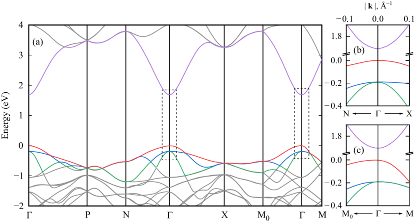
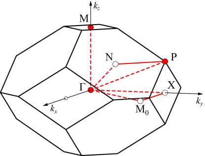
To describe electrons and holes confined in the AgInS2 nanocrystal we use the density functional theory and the multiband -theory. Luttinger (1956) The band structure and the Brillouin zone of AgInS2 are shown in Figs. 1 and 2, respectively. As in the case of CuInS2, Shabaev et al. (2015) our simulations of AgInS2 have shown that the spin-orbit splitting meV is much smaller than the energy difference between quantum-confined hole states ( meV, see Fig. 3), so we can use the spin unpolarized functionals.
The band structure was obtained from the ab initio simulation with the vasp code Kresse and Furthmüller (1996) and the B3LYP hybrid exchange functional Becke (1993)
The calculation was performed on a grid of points with 120 bands. The bands were interpolated with the wannier90 program.Mostofi et al. (2014) The calculated direct band gap at the point eV is close to the experimental one at the room temperature eV You et al. (2002); Kameyama et al. (2015). In comparison to B3LYP, simulations with the HSE06 hybrid functional and G0W0 approximation yield similar effective masses and , but smaller values of the fundamental band gap: eV and eV.
The crystal-field splitting comes from the breakdown of the cubic symmetry in the chalcopyrite structure, and exists even in the absence of the spin-orbit coupling.Shay et al. (1974) The crystal-field split band (cs) in AgInS2 lies above the bands of heavy (hh) and light holes (lh). Limpijumnong and Lambrecht (2002) Thus the calculated splitting energy is negative, meV, and the order of valence bands is reverse to the one in CuInS2. Shabaev et al. (2015)
To calculate the Luttinger parameters,Luttinger (1956) we fit the lowest conduction (c) and the highest valence bands (cs, hh, and lh) along the high-symmetry directions to points M, M0, and X by parabolic functions of . The close-up views for these directions in the vicinity of point are shown in Figs. 1(b) and 1(c). The effective masses found from the fitting procedure are summarized in Table 1. These masses are in close agreement with the previous DFT calculations.Huang and Persson (2014); Liu and Hua (2015)
In the the -method, Kane (1956) the electron energy is given byEfros and Rosen (2000); Shabaev et al. (2015)
| (1) |
where is the mass of a free electron, is the Kane energy, and is the contribution of the remote bands to the electron effective mass. The best fit of our first-principle spectrum is obtained for eV and . For the effective mass of electron is .
In spherical nanocrystals of radius and an infinitely high confining potential, the energy and wave function of the electron on the ground level can be written as follows:
| (2) |
and
| (3) |
where .
The valence band structure can be constructed by the method of invariants introduced by Luttinger.Luttinger (1956) The parameters of this Hamiltonian were obtained from our ab initio simulations. Following Shabaev et al. (2015), we neglect the hole energy spectrum warping and find the confined valence band levels using the first-order perturbation theory with the spherically-symmetric Hamiltonian:
| (4) |
where (Ref. Lipari and Baldereschi, 1970), , , and are the Luttinger parameters,Luttinger (1956) and and are the momentum and the spin-1 matrix operators, respectively.
The point group symmetry of AgInS2 allows for additional invariant terms , which can be added to the Hamiltonian in Eq. (4). For the band structure obtained from our DFT calculation, we found that the valence band spectrum can be described by the Hamiltonian in Eq. (4) with the following addition to the cubic Hamiltonian quadratic invariants:Limpijumnong and Lambrecht (2002)
| (5) |
where , , , plus four additional Luttinger parameters , , , and are associated with the effective masses of the three valence bands in various crystallographic directions.
By applying the fitting procedure to our first-principle results, we obtain the data summarized in Table 2. Parameters , , and are close to the parameters obtained for data fitting of CuInS2 by Shabaev et al. (2015)
In a spherical nanocrystal, one can separate variables for each state with total angular momentum . Here, we are interested only in the manifold of the lowest energy levels of holes with angular momentum . Using techniques developed in Ref. Ekimov et al., 1986 we find that the wave functions of even and odd states with and angular momentum projection can be written asShabaev et al. (2015)
| (6) |
and
| (7) |
where are the spherical harmonics, are the Clebsch-Gordan coefficients, and are the spinors representing the eigenvectors of the operator. Hereafter, all the primed symbols are related to the odd hole states, while the non-primed symbols — to the even states.
Energies of these states without perturbation of potential depend on Luttinger parameters and dimensionless coefficients and . Here, is the first zero of the Bessel function and depends on the ratio . For even and odd states we have
| (8a) | |||
| (8b) | |||
The fine structure of these states can be obtained as a perturbation associated with the deviation from cubic symmetry by the Hamiltonian in Eq. (5). These energy perturbations, and , are determined as follows:
| (9) |
where for one should replace by .
Finally, using the Luttinger parameters from Table 2, we find the explicit values of perturbed energies and :
| (10a) | ||||
| (10b) | ||||
| (10c) | ||||
| (10d) | ||||
Figure 3 shows energy corrections determining the fine structure of the hole states. In contrast to the CuInS2 nanocrystals, where the lowest energy state without the spin-orbit coupling is the optically inactive state,Shabaev et al. (2015) the lowest energy state in AgInS2 is the optically active -state. This is because the crystal splitting meV in AgInS2 has an opposite sign and larger absolute value. The order of other quantum-confined states is also different in these two chalcopyrite compounds and determined primarily by the crystal splitting.
II.2 Polaron and Coulomb shifts
The Hamiltonian of electronic and vibrational subsystems of a nanocrystal is given by Kittel (1987); Rukhlenko et al. (2011); Baimuratov et al. (2014)
| (11) |
where the first two terms correspond to the noninteracting electron-hole pairs and LO phonons, whereas the last one describes their interaction. Creation (annihilation) of electron-hole pairs in the state with the energy is described by the operators (), where and are the electron and hole energies, respectively, is the band gap of the bulk semiconductor, is the Coulomb interaction between the electron and hole. LO phonons with the energy and wave vector are described by the creation (annihilation) operators .
The polar electron-phonon interaction in nanocrystals induces intraband transitions between the states of electron-hole pairs. We take into account only the diagonal part. This allows representing the electron-phonon Hamiltonian as
| (12) |
where is the electron charge, , and are the reduced, low- and high-frequency dielectric permitivities of the bulk semiconductor, is the nanocrystal volume, and Fourier component of the charge carrier density is given by
| (13) |
It should be noted that the spatial quantization of the optical vibrational eigenmodes can be easily done, but it gives qualitatively similar results.Fedorov et al. (1997)
We start from the elimination of the electron and hole coordinates by averaging over the envelopes of electrons and holes Ipatova et al. (2001)
| (14) |
The unified consideration of interacting electrons and phonons leads to the formation of polarons.Pekar (1983) Their eigenstates can be found via diagonalization of the Hamiltonian (14), , with the Lee–Low–Pines transformation Lee et al. (1953)
| (15) |
By replacing the summation over by integration in (15), we find the energy of electron-hole pair renormalized by electron-phonon interaction, where the polaron binding energy is
| (16) |
In the case of spherical nanocrystal of radius , it is convenient to rewrite Eq. (16) in the dimensionless coordinates and as
| (17) |
where
| (18) |
The Coulomb interaction is considered as a perturbation to energy
| (19) |
where
| (20) |
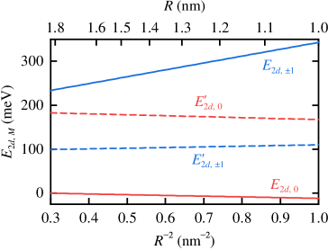
Using Eqs. (3), (6), and (7), we find the dimensionless parameters and as well as corrections and to the energy spectrum of the electron-hole pair with electron and holes of angular momentum in nanocrystals of radius nm. These results are summarized in Table 3.
| parity | ||||||
|---|---|---|---|---|---|---|
| even | ||||||
| even | ||||||
| odd | ||||||
| odd |
The polaron binding energy is relatively small, with the most significant value corresponding to the odd hole state with angular momentum projection , whereas two even hole states possess the lowest binding energies. This is because even hole states are determined by the -type wave functions, while odd hole states are formed by the wave functions of -type.
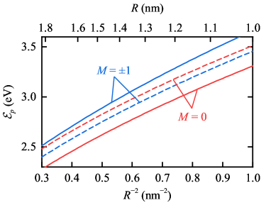
Figure 4 shows size dependencies of the electron-hole pair energies shifted by the Coulomb interaction and the polaron binding energy. For all the considered electron-hole pairs with an electron in the state the energy difference between their levels depends only on the energy of holes and shifts and . Electron-hole pairs with even hole states are optically active, while the pairs with odd hole states are not. The spin-orbit coupling is slightly activated optically by its admixture to the optically active even hole level.Shabaev et al. (2015) In any case, light absorption for optical transition between the state and odd hole states is rather weak. Therefore, the lowest optically active level corresponds to the odd hole state with and the lowest optically passive level is related to even hole state with . We emphasize that the mechanism of Stokes shift proposed by Shabaev et al. (2015) for CuInS2 does not work for AgInS2, due to the obtained reverse order of the lowest-energy levels (the lowest level is allowed in AgInS2).
II.3 Trap states
Due to the structural complexity of ternary nanocrystals, many trap states are commonly observed. The possible traps in these ternary compounds, namely donors and acceptors, are related to vacancies and interstitial atoms of Ag, In, and S,Hamanaka et al. (2011) or other charge defects such as substitution of In on the position of Ag and vice versa.Chevallier et al. (2017) If the nanocrystal has a shell of ZnS, there are additional mechanisms of defect formation via Zn ions.Mao et al. (2013)
Without loss of generality, we consider an acceptor trap with charge ( is integer number). We choose hole to be trapped charge carrier because its effective mass is much larger than that of an electron. We assume that the trap states are described by binding energy and the trial wave function
| (21) |
where is the trap position, and is the localization parameter of hole in the trap.
The total energy of an electron-hole pair in this state is given by
| (22) |
By assuming that the hole is strongly localized (), and the trap state is bulk-like, i.e. it does not strongly depend on the nanocrystal properties, we can write the binding energy of an electron-hole pair on the defect as follows:
| (23) |
where the first term is the sum of the trapped hole kinetic energy and its Coulomb interaction with acceptor, the second term is the energy of the Coulomb interaction between the electron and the acceptor after trapping of the hole,
| (24) |
, is the cosine integral, and the last term is the polaron binding energy for the trap state
| (25) |

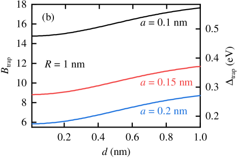
From Eqs. (18), (3), and (21) we find the strength of polaron effects for the states with trapped holes . We plot this dimensionless strength in Fig. 5, which shows that the obtained values of 10–70 are by a few orders of magnitude larger than in the case of non-trapped states. We calculate them for three different localization parameters, , and nm and for two defect positions . With the localization of a hole on the trap, the strength of polaron effect grows linearly due to the decrease of wave function overlapping of electron and hole. Fig. 5(b) shows that the maximal polaron strength relates to . For the estimation of polaron binding energy we use AgInS2 nanocrystal of nm. The obtained values of are shown on the right axis in Fig. 5(b).
III Photoluminescence and Stokes shift
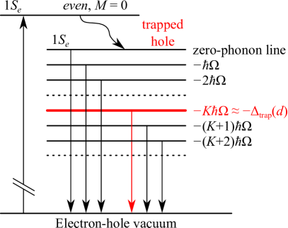
Absorption and photoluminescence processes involving trapped states are schematically shown in Fig. 6. First, the absorbed light creates an electron-hole pair, which is relaxed to the lowest energy non-trapped state. Second, the acceptor traps a hole, and finally, an electron recombines with the trapped hole and emits one photon and phonons. In the approximation of dispersionless phonons, , the Stokes shift has a contribution from the double polaron binding energy because the phonon replica with the energy has the highest intensity in the photoluminescence spectrum.Ipatova et al. (2001) Here, is the Huang–Rhys parameter.Huang et al. (1950) The probability of emission of photon of frequency and phonons can be calculated from the harmonic oscillator approximationLandau and Lifshits (1965)
| (26) |
where is the interband transition matrix element of the coordinate operator between the Bloch functions, which is given by , and is the overlap integral of the electron and hole wave functions.
Assuming that the first absorption peak relates to the even hole level with and the electron in the -state and that the maximum of the photoluminescence spectrum relates to the -phonon replica of the trapped state, we find the following expression for the Stokes shift of nanocrystal with a trapped hole
| (27) |
If we neglect small polaron shift , we obtain
| (28) |
Notably, the Stokes shift depends on the kinetic term of the nontrapped hole .
In recent experiments, the photoluminescence spectra from single nanocrystals of radius 1–2 nm demonstrate wide FWHM, –360 meV.Stroyuk et al. (2019) The phonon energy for this material is about 33 meV,Hamanaka et al. (2011), which leads to quite a large number of .
Assuming the finite linewidth of the replica and , we can rewrite Eq. (26) as
| (29) |
The FWHM of this spectra is . We estimate –21 and –700 meV by taking FWHM for a single nanocrystal as 240–360 meV from experimental data and find that the localization parameter is within the range of 0.08–0.14 nm.
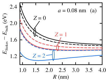
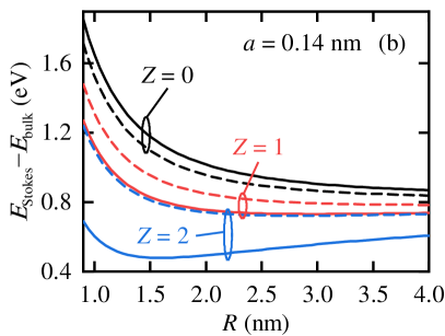
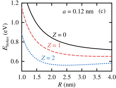
Finally, to determine the Stokes shift we consider acceptors with charges (the noncharged acceptor with is related to the self-trapped model). The results for Stokes shifts without a constant contribution for defect positions and the localization parameters nm and nm are shown in Figs. 7(a) and 7(b).
To compare our numerically calculated Stokes shifts for nanocrystal ensembles with experimental data, we make a few additional assumptions. First, we take the averaged value of the fitted data nm as a localization parameter. Second, for spherical nanocrystals the probability of finding a defect at position is proportional to whereas the overlap integral scales like . After taking the derivative of the product , we solve the transcendental equation and find that the largest contribution in ensemble comes from the nanocrystals with .
To roughly estimate the value of we assume the bulk limit and find that . The binding energy of acceptor for bulk AgInS2 was measured in several experiments. For instance, the photoluminescence upon optical transitions with meV was associated with a deep level of vacancies Ag, interstitial atoms of S,You et al. (2001) or other point defects –190 meV.Hamanaka et al. (2011) We take the value meV derived by Hamanaka et al. (2011), which is close to averaged value of the above mentioned experimental works. This simple analysis gives meV.
The results of fitting for the acceptor with charges are shown in Fig. 7(c). For all three values of charge we find the giant Stokes shifts of 0.5–1 eV, which are in good agreement with experimental values.Hamanaka et al. (2011); Jeong et al. (2017); Raevskaya et al. (2017); Stroyuk et al. (2019, 2018) According to our simulations, the Stokes shift decreases with the QD size [see Fig. 7(c)]. This dependence has been observed for II–VI and IV–VI binary nanoparticles, such as CdSe and CdS nanoparticles with excitonic emission. Efros et al. (1996); Yu et al. (2003) Stroyuk et al. (2018) demonstrated a similar dependency for aqueous glutation-capped size-selected AgInS2/ZnS nanoparticles with diameters of 2–3 nm but explained it by assuming that the number of phonons involved in the optical process decreases with the size of nanoparticles. On the other hand, the reported Stokes shifts of aqueous AgInS2/ZnS QDs capped with mercaptoacetic acid are nearly constant in the 2.0–3.5 nm diameter range.Raevskaya et al. (2017) This controversy between the experimental results could be explained by the insufficient accuracy of band gap measurements due to the absence of a sharp first peak in the absorption spectra. Martynenko et al. (2019)
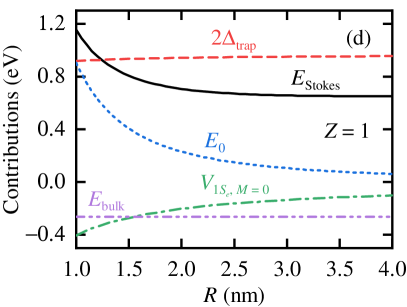
Figure 7(d) compares different contributions to the Stokes shift for a hole trapped by an acceptor with . There are two positive contributions: the doubled polaron binding energy and the kinetic term of the non-trapped hole . The first one weakly grows with whereas the second one decreases as . The other two contributions are negative, the first one is related to , and the second one is the Coulomb interaction of the non-trapped state decreasing with nanoparticle size as .
Our model predicts that the size dependence of the Stokes shift is determined by two qualitatively different contributions. The first one, , originates from the size-dependent part of a kinetic term . The second contribution, , is related to the Coulomb interaction. The first term is always positive, whereas the sign of the second may change with charge parameter and defect position . Remarkably, the polaron binding energy gives one of the main contributions to the Stokes shift and does not significantly dependent on the nanocrystal size. Figure 7(d) shows that only for small nanocrystals ( nm) the kinetic term closely approaches the value of .
IV Conclusions
We have developed a theoretical model of a giant Stokes shift in AgInS2 nanocrystals with trapped charge carriers. From the calculations with the B3LYP hybrid functional, we determined the Luttinger parameters and calculated the energies and wave functions of electrons and holes in spherical nanocrystals using the multiband -theory. Kane (1956); Luttinger (1956); Shabaev et al. (2015) For the first time, we calculated the size dependencies of the lowest electron-hole pairs with both Coulomb and polaron corrections. We took into account the presence of one point defect acceptor trapping holes from the lowest non-trapped state. The comparison of our results with experimental photoluminescence spectra for a single nanocrystal and the calculation of polaron binding energy for a trapped hole confirmed that the hole must be strongly localized with characteristic lengths of –0.14 nm.
Our simulations quantitatively reproduce the experimentally measured Stokes shift ( eV) for a state with the hole localized on acceptors ( nm) with charges and radial position . The main contribution is given by the polaron binding energy, eV. The size dependence of the Stokes shift primarily originates from the kinetic term of initially non-trapped hole and Coulomb interaction in a confined quantum system.
V Acknowledgements
A. S. B. has received funding from the European Union’s Framework Programme for Research and Innovation Horizon 2020 (2014–2020) under the Marie Skłodowska–Curie Grant Agreement No. 754388 and from LMU Munich’s Institutional Strategy LMUexcellent within the framework of the German Excellence Initiative (No. ZUK22). I. V. M., A. V. B, A. V. F., and I. D. R. were partially funded by the Federal Target Program for Research and Development of the Ministry of Education and Science of the Russian Federation, grant no. 14.587.21.0047 (ID RFMEFI58718X0047). S. Yu. K. acknowledges support from the Austrian Science Fund (FWF) within the Lise Meitner Project No. M2198-N30. The numerical calculations were partially performed at the Vienna Scientific Cluster (VSC-3).
References
- Bai et al. (2019) X. Bai, F. Purcell-Milton, and Y. K. Gun’ko, Nanomaterials 9, 85 (2019).
- Girma et al. (2017) W. M. Girma, M. Z. Fahmi, A. Permadi, M. A. Abate, and J.-Y. Chang, J. Mater. Chem. B 5, 6193 (2017).
- Kolny-Olesiak and Weller (2013) J. Kolny-Olesiak and H. Weller, ACS Appl. Mater. Interfaces 5, 12221 (2013).
- Ulusoy et al. (2016) M. Ulusoy, R. Jonczyk, J.-G. Walter, S. Springer, A. Lavrentieva, F. Stahl, M. Green, and T. Scheper, Bioconj. Chem. 27, 414 (2016).
- Xu et al. (2016) G. Xu, S. Zeng, B. Zhang, M. T. Swihart, K.-T. Yong, and P. N. Prasad, Chem. Rev. 116, 12234 (2016).
- Pietryga et al. (2016) J. M. Pietryga, Y.-S. Park, J. Lim, A. F. Fidler, W. K. Bae, S. Brovelli, and V. I. Klimov, Chem. Rev. 116, 10513 (2016).
- Bergren et al. (2018) M. R. Bergren, N. S. Makarov, K. Ramasamy, A. Jackson, R. Guglielmetti, and H. McDaniel, ACS Energy Lett. 3, 520 (2018).
- Aldakov et al. (2013) D. Aldakov, A. Lefrancois, and P. Reiss, J. Mater. Chem. C 1, 3756 (2013).
- Mao et al. (2011) B. Mao, C.-H. Chuang, J. Wang, and C. Burda, J. Phys. Chem. C 115, 8945 (2011).
- Raevskaya et al. (2017) A. Raevskaya, V. Lesnyak, D. Haubold, V. Dzhagan, O. Stroyuk, N. Gaponik, D. R. T. Zahn, and A. Eychmüller, J. Phys. Chem. C 121, 9032 (2017).
- Song et al. (2016) J. Song, C. Ma, W. Zhang, X. Li, W. Zhang, R. Wu, X. Cheng, A. Ali, M. Yang, L. Zhu, R. Xia, and X. Xu, ACS Appl. Mater. Interfaces 8, 24826 (2016).
- Stroyuk et al. (2018) O. Stroyuk, A. Raevskaya, F. Spranger, O. Selyshchev, V. Dzhagan, S. Schulze, D. R. T. Zahn, and A. Eychmüller, J. Phys. Chem. C 122, 13648 (2018).
- van der Stam et al. (2016) W. van der Stam, A. C. Berends, and C. de Mello Donega, Chem. Phys. Chem. 17, 559 (2016).
- Stroyuk et al. (2019) O. Stroyuk, F. Weigert, A. Raevskaya, F. Spranger, C. Würth, U. Resch-Genger, N. Gaponik, and D. R. T. Zahn, J. Phys. Chem. C 123, 2632 (2019).
- Martynenko et al. (2019) I. V. Martynenko, A. S. Baimuratov, F. Weigert, J. X. Soares, L. Dhamo, I. Doerfel, J. Pauli, P. Nickl, I. D. Rukhlenko, and A. V. Baranov, Nano Res. accepted (2019).
- Zang et al. (2017) H. Zang, H. Li, N. S. Makarov, K. A. Velizhanin, K. Wu, Y.-S. Park, and V. I. Klimov, Nano Lett. 17, 1787 (2017).
- Whitham et al. (2016) P. J. Whitham, A. Marchioro, K. E. Knowles, T. B. Kilburn, P. J. Reid, and D. R. Gamelin, J. Phys. Chem. C 120, 17136 (2016).
- Chang et al. (2012) J.-Y. Chang, G.-Q. Wang, C.-Y. Cheng, W.-X. Lin, and J.-C. Hsu, J. Mater. Chem. 22, 10609 (2012).
- Deng et al. (2012) D. Deng, Y. Chen, J. Cao, J. Tian, Z. Qian, S. Achilefu, and Y. Gu, Chem. Mater. 24, 3029 (2012).
- Evstigneev et al. (2019) R. V. Evstigneev, P. S. Parfenov, A. Dubavik, S. A. Cherevkov, A. V. Fedorov, I. Martynenko, U. Resch-Genger, E. V. Ushakova, and A. V. Baranov, Nanotechnology 30, 195501 (2019).
- Leach and Macdonald (2016) A. D. P. Leach and J. E. Macdonald, J. Phys. Chem. Lett. 7, 572 (2016).
- Nagamine et al. (2018) G. Nagamine, H. B. Nunciaroni, H. McDaniel, A. L. Efros, C. H. de Brito Cruz, and L. A. Padilha, Nano Lett. 18, 6353 (2018).
- Xia et al. (2018) C. Xia, W. Wu, T. Yu, X. Xie, C. van Oversteeg, H. C. Gerritsen, and C. de Mello Donega, ACS Nano 12, 8350 (2018).
- Hamanaka et al. (2011) Y. Hamanaka, T. Ogawa, M. Tsuzuki, and T. Kuzuya, J. Phys. Chem. C 115, 1786 (2011).
- Jeong et al. (2017) S. Jeong, H. C. Yoon, N. S. Han, J. H. Oh, S. M. Park, B. K. Min, Y. R. Do, and J. K. Song, J. Phys. Chem. C 121, 3149 (2017).
- Chen et al. (2018) B. Chen, N. Pradhan, and H. Zhong, J. Phys. Chem. Lett. 9, 435 (2018).
- Suriyawong et al. (2016) N. Suriyawong, B. Aragaw, J.-B. Shi, and M.-W. Lee, J. Colloid Interface Sci. 473, 60 (2016).
- Hu et al. (2015) X. Hu, R. Kang, Y. Zhang, L. Deng, H. Zhong, B. Zou, and L.-J. Shi, Opt. Express 23, A858 (2015).
- Klimov et al. (2016) V. I. Klimov, T. A. Baker, J. Lim, K. A. Velizhanin, and H. McDaniel, ACS Photonics 3, 1138 (2016).
- Meinardi et al. (2015) F. Meinardi, H. McDaniel, F. Carulli, A. Colombo, K. A. Velizhanin, N. S. Makarov, R. Simonutti, V. I. Klimov, and S. Brovelli, Nat. Nanotechnol. 10, 878 (2015).
- Wu et al. (2018) K. Wu, H. Li, and V. I. Klimov, Nature Photonics 12, 105 (2018).
- Martynenko et al. (2017) I. V. Martynenko, A. P. Litvin, F. Purcell-Milton, A. V. Baranov, A. V. Fedorov, and Y. K. Gun’ko, J. Phys. Chem. B 5, 6701 (2017).
- Fuhr et al. (2017) A. S. Fuhr, H. J. Yun, N. S. Makarov, H. Li, H. McDaniel, and V. I. Klimov, ACS Photonics 4, 2425 (2017).
- Knowles et al. (2015) K. E. Knowles, H. D. Nelson, T. B. Kilburn, and D. R. Gamelin, J. Am. Chem. Soc. 137, 13138 (2015).
- Shabaev et al. (2015) A. Shabaev, M. J. Mehl, and A. L. Efros, Phys. Rev. B 92, 035431 (2015).
- Kane (1956) E. Kane, J. Phys. Chem. Sol. 1, 82 (1956).
- Luttinger (1956) J. M. Luttinger, Phys. Rev. 102, 1030 (1956).
- Aroyo et al. (2011) M. I. Aroyo, J. Perez-Mato, D. Orobengoa, E. Tasci, G. De La Flor, and A. Kirov, Bulg. Chem. Commun. 43, 183 (2011).
- Kresse and Furthmüller (1996) G. Kresse and J. Furthmüller, Phys. Rev. B 54, 11169 (1996).
- Becke (1993) A. D. Becke, J. Chem. Phys. 98, 5648 (1993).
- Mostofi et al. (2014) A. A. Mostofi, J. R. Yates, G. Pizzi, Y.-S. Lee, I. Souza, D. Vanderbilt, and N. Marzari, Comp. Phys. Comm. 185, 2309 (2014).
- You et al. (2002) S. You, K. Hong, B. Lee, T. Jeong, C. Youn, J. Park, and S. Baek, J. Cryst. Growth 245, 261 (2002).
- Kameyama et al. (2015) T. Kameyama, T. Takahashi, T. Machida, Y. Kamiya, T. Yamamoto, S. Kuwabata, and T. Torimoto, J. Phys. Chem. C 119, 24740 (2015).
- Shay et al. (1974) J. L. Shay, B. Tell, L. M. Schiavone, H. M. Kasper, and F. Thiel, Phys. Rev. B 9, 1719 (1974).
- Limpijumnong and Lambrecht (2002) S. Limpijumnong and W. R. L. Lambrecht, Phys. Rev. B 65, 165204 (2002).
- Huang and Persson (2014) D. Huang and C. Persson, Chem. Phys. Lett. 591, 189 (2014).
- Liu and Hua (2015) J. Liu and E. Hua, Mater. Sci. Semicond. Process 40, 446 (2015).
- Efros and Rosen (2000) A. L. Efros and M. Rosen, Ann. Rev. Mater. Sci. 30, 475 (2000).
- Lipari and Baldereschi (1970) N. O. Lipari and A. Baldereschi, Phys. Rev. Lett. 25, 1660 (1970).
- Ekimov et al. (1986) A. Ekimov, A. Onushchenko, M. Raikh, and A. L. Efros, Sov. Phys. JETP 63, 1054 (1986).
- Kittel (1987) C. Kittel, Quantum Theory of Solids (Wiley, 1987).
- Rukhlenko et al. (2011) I. D. Rukhlenko, A. V. Fedorov, A. S. Baymuratov, and M. Premaratne, Opt. Expr. 19, 15459 (2011).
- Baimuratov et al. (2014) A. S. Baimuratov, I. D. Rukhlenko, M. Y. Leonov, A. G. Shalkovskiy, A. V. Baranov, and A. V. Fedorov, Opt. Expr. 22, 19707 (2014).
- Fedorov et al. (1997) A. V. Fedorov, A. V. Baranov, and K. Inoue, Phys. Rev. B 56, 7491 (1997).
- Ipatova et al. (2001) I. P. Ipatova, A. Y. Maslov, and O. V. Proshina, Europhys. Lett. 53, 769 (2001).
- Pekar (1983) S. Pekar, Crystal Optics and Additional Light Waves, Frontiers in Physics (Benjamin/Cummings Publishing Company, 1983).
- Lee et al. (1953) T. D. Lee, F. E. Low, and D. Pines, Phys. Rev. 90, 297 (1953).
- Márquez and Rincón (1995) R. Márquez and C. Rincón, Phys. Status Solidi B 191, 115 (1995).
- Chevallier et al. (2017) T. Chevallier, A. Benayad, G. Le Blevennec, and F. Chandezon, Phys. Chem. Chem. Phys. 19, 2359 (2017).
- Mao et al. (2013) B. Mao, C.-H. Chuang, F. Lu, L. Sang, J. Zhu, and C. Burda, J. Phys. Chem. C 117, 648 (2013).
- Huang et al. (1950) K. Huang, A. Rhys, and N. F. Mott, Proc. Royal Soc. A 204, 406 (1950).
- Landau and Lifshits (1965) L. D. Landau and E. M. Lifshits, Quantum Mechanics: Non-Relativistic Theory, Vol. 3 (Pergamon press, 1965).
- You et al. (2001) S. H. You, K. J. Hong, C. J. Youn, T. S. Jeong, J. D. Moon, H. S. Kim, and J. S. Park, J. Appl. Phys. 90, 3894 (2001).
- Efros et al. (1996) A. L. Efros, M. Rosen, M. Kuno, M. Nirmal, D. J. Norris, and M. Bawendi, Phys. Rev. B 54, 4843 (1996).
- Yu et al. (2003) Z. Yu, J. Li, D. B. O’Connor, L.-W. Wang, and P. F. Barbara, J. Phys. Chem. B 107, 5670 (2003).