YBa2Cu3O7/La2/3X1/3MnO3 (X: Ca, Sr) based Superconductor/Ferromagnet/Superconductor junctions with memory functionality
Abstract
Complex oxides exhibit a variety of unusual physical properties, which can be used for designing novel electronic devices. Here we fabricate and study experimentally nano-scale Superconductor/Ferromagnet/Superconductor junctions with the high- cuprate superconductor YBa2Cu3O7 and the colossal magnetoresistive (CMR) manganite ferromagnets La2/3X1/3MnO3 (X: Ca or Sr). We demonstrate that in a broad temperature range the magnetization of a manganite nanoparticle, forming the junction interface, switches abruptly in a mono-domain manner. The CMR phenomenon translates the magnetization loop into a hysteretic magnetoresistance loop. The latter facilitates a memory functionality of such a junction with just a single CMR ferromagnetic layer. The orientation of the magnetization (stored information) can be read out by simply measuring the junction resistance in an applied magnetic field. The CMR facilitates a large read-out signal in a small applied field. We argue that such a simple single layer CMR junction can operate as a memory cell both in the superconducting state at cryogenic temperatures and in the normal state up to room temperature.
pacs:
74.50.+r, 85.25.CpI Introduction
The competition of the antagonistic phenomena of spin-singlet superconductivity and spin-polarized ferromagnetism in superconductor/ferromagnet (S/F) heterostructures leads to several unusual phenomena, which are interesting both for fundamental and applied research Buzdin; Efetov2005; Golubov2007; Eschrig_2015; Sidorenko_2017. In particular, hybrid S/F structures are promising candidates for the creation of a scalable and dense cryogenic memory. Such a memory is needed for a superconducting digital exaflop computer, which can significantly outperform a semiconducting analog both in speed and energy efficiency Likharev_1991; Mukhanov_2011; Holmes_2013. At present there is no suitable cryogenic random access memory (RAM) for the superconducting computer. This is considered to be the “main obstacle to the realization of high performance computer systems and signal processors based on superconducting electronics” Ortlepp_2014. Several new concepts for scalable, nm-sized superconducting RAM, involving hybrid S/F structures, were proposed recently TLarkin_2012; Herr_2018; Sidorenko_2013; Dresselhaus_2014; Nevirkovets_2014; Golod_2015; Birge_2017. The non-volatile memory function in ferromagnets is naturally provided by the finite coercive field for the remagnetization of the ferromagnetic particle, and the information is stored in the orientation of the magnetization. The conventional (room temperature) magnetic RAM Parkin_2006; MRAM_2017 contains a multilayered spin-valve structure, in which the information is stored in terms of the relative orientation of the magnetization of the F-layers and the readout signal is provided by the orientation dependence of the resistance. In S/F memory cells the information is also stored in the orientation, but the readout parameter is the critical superconducting current of the device.
One of the unusual phenomena in S/F spin-valves is the possibility to generate a spin-triplet superconducting order parameter in the F-layers. This should occur in the non-collinear state of the S/F spin-valve and should lead to an enhancement of the supercurrent through the spin-valve Buzdin; Efetov2005; Golubov2007; Blamire2010; Khaire2010; Iovan_2014; Iovan_2017. It is anticipated that this phenomenon should be most spectacular in a fully spin-polarized ferromagnet, which would not be able to accommodate spin-singlet Cooper pairs Keizer2006; Aarts; Hu_LMO_Triplet2009; Dybko_LMO_Triplet2009; Kalcheim2011; Visani2012; Golod_2013; Ivan_2014. The full spin polarization occurs naturally in half-metallic ferromagnets such as the manganite perovskite-oxides considered in this work.
Perovskite-oxides and related oxides with strongly correlated electrons are known for their complex phase diagrams, with coexisting and often competing interactions and orders that give rise to a wealth of unconventional states with outstanding properties Corr_review; Imada_1998; Dagotto_2007. The most prominent examples are the high-temperature superconductivity (HTSC) Muller1986 in the cuprates and the colossal magetoresistance (CMR) in the manganites Samwer_1993 but there is also a wide range of ferro- and antiferro- magnetic, ferroelectric, multiferroic, charge/spin density wave, and orbital ordered states. Their versatile physical properties can be readily tuned by chemical substitution, which affects the carrier concentration and/or the crystal structure, external pressure, stress, temperature and electric Simcek_2016 and magnetic fields. Such a tunability is very interesting for fundamental research of unconventional states of matter as well as for designing novel electronic devices with new functionality. However, the sensitivity of the perovskites to structural modifications also requires an accurate control of the thin film structure and the crystalline and chemical quality. In recent years it has been demonstrated that such control can be achieved via the heteroepitaxial growth of complex oxide multilayers with sequentially matching crystal structures Christen_2008; Tokura_2012; Bibes_2011. Several all-perovskite electronic devices have already been demonstrated, such as solar cells Solarcell1; Solarcell2, memristors, and resistive RAM Memristor1.
Heteroepitaxial thin film multilayers of the cuprate HTSC YBa2Cu3O7-x (YBCO) and the ferromagnetic manganites La2/3Ca1/3MnO3+δ (LCMO) and La2/3Sr1/3MnO3+δ (LSMO) can be readily grown, thanks to the good matching of their crystal structures GalassoBook; Habermeier_2002; Varela_2003; Malik_2012; Goldman_2001; Sawicki_1997; Ovsyannikov_2017. High superconducting critical temperatures = 90 K of YBCO and Curie temperature = 270/370 K of LCMO/LSMO enables operation of S/F devices based on such heterostructures at the liquid nitrogen temperature, which is advantageous for various potential future applications.
In this work we fabricate and study experimentally complex oxide YBCO/LCMO/YBCO and YBCO/LSMO/YBCO nano-scale junctions with a minimum feature size of nm. We demonstrate that such SFS junctions with a single colossal magnetoresitive F-layer can be used as memory cells. In such a S-CMR-S memory the information is stored in the orientation of the magnetization of the single F-layer. However, in contrast to previous memory prototypes based on SFS Josephson junctions, the readout in our devices is based entirely on the CMR phenomenon measured across the junction. We demonstrate that the CMR effect allows us to reconstruct the magnetization loop of a single F-nanoparticle that forms the junction barrier. The magnetization loops are characterized by an abrupt switching between saturated magnetization states, typical for a mono-domain state of the ferromagnetic interlayer. Since YBCO is a high temperature superconductor with K, our devices can operate comfortably at liquid nitrogen temperatures. Furthermore, since we are not using the superconducting critical current for readout, such a device can operate above and even at room temperature. Therefore, we conclude that such cuprate/manganate heterostructures can be used to create complex oxide electronic and spintronic devices both superconducting at cryogenic temperatures and normal conducting at room temperature.
II Experimental
SFS trilayers composed of YBa2Cu3O7 and La2/3Ca1/3MnO3 (LCMO) or La2/3Sr1/3MnO3 (LSMO) were grown by pulsed laser deposition (PLD) on (0 0 1)-oriented La0.3Sr0.7Al0.65Ta0.35O3 (LSAT) substrates (Crystec) using an excimer KrF laser ( = 248 nm, ts = 25 ns). The trilayer denoted as LC_10 has the structure YBCO (100 nm) / LCMO (10 nm) / YBCO (100 nm), while the one labelled LS_11 is YBCO (100 nm) / LSMO (11 nm) / YBCO (100 nm). They were grown at 840∘C in a partial pressure of 0.34 mbar of O2 with a laser fluency of 1.42 Jcm-2 and a frequency of 7 Hz. Subsequently, the samples were cooled to 700∘C, where the pressure was increased to 1 bar of pure O2, and further cooled at a rate of to 30∘C per minute to a first in situ annealing step at 485∘C and a second one at 400∘C (each for 1 hour) to ensure a full oxygenation of the trilayer. Finally, the trilayers were coated with 100 nm of Au (using a thermal evaporator) as protective layer during the device fabrication.
The dc magnetization was measured with the vibrating sample magnetometer (VSM) of a physical properties measurement system by Quantum Design (QD-PPMS). The magnetic field was applied parallel to the film surface. The magnetic signal from the LSAT substrate was subtracted to obtain the magnetization of the film which in the presentation below is scaled to a magnetic moment per Mn atom. Below the superconducting transition of YBCO the interpretation of the VSM data is complicated by the diamagnetic signal of YBCO. Therefore, we show in the following only the data above 90 K.
The SFS junctions were made from the trilayers using nanofabrication techniques. First, finger-like electrodes of m in width were defined on the samples by optical lithography and cryogenic reactive ion etching at -50∘C (cryo-RIE) in Ar plasma. Cryogenic etching preserves the oxygen content in the oxides and minimizes the deterioration of the samples. Next, the samples were transferred to a dual beam scanning electron microscope (SEM) - Ga+ focused ion beam (FIB) system. Using the FIB we made narrow bridges in the electrodes of m length and 275 nm width. Subsequently, the sample was tilted to a glazing angle with respect to the FIB column, and two sidecuts were made to interrupt the bottom and top YBCO layers in the bridge, forcing the current flow through the F barrier. Details of the fabrication procedure can be found in Ref. Golod_2013.
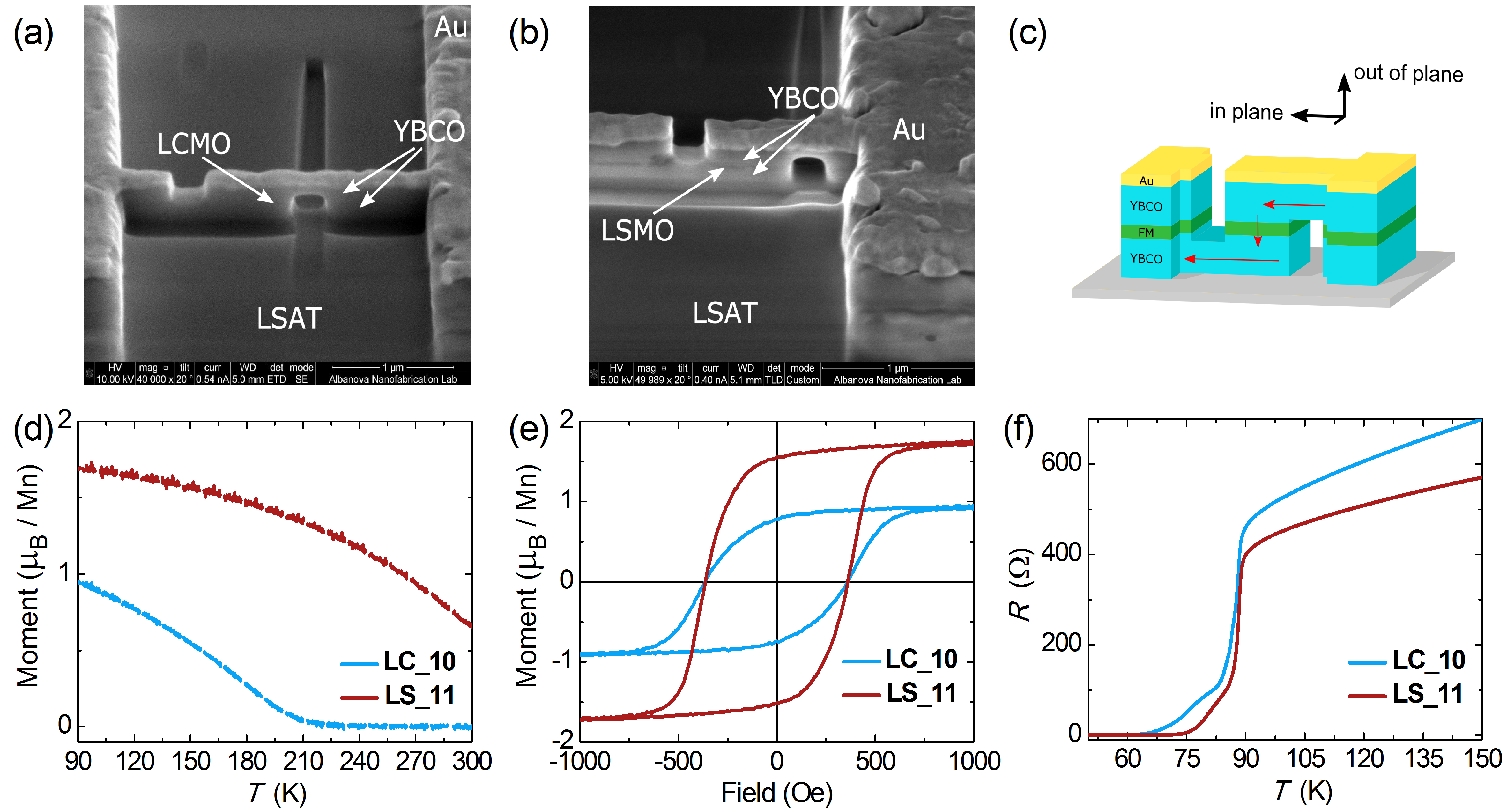
Figures 1 (a) and (b) show SEM images of junctions on samples LC_10 and LS_11, respectively. In Fig. 1 (a) the interrupting cuts are 700 nm apart, thus creating a nm2 LCMO junction. For LS_11 in Fig. 1 (b), the LSMO junction is nm2. A sketch of the junctions that consist of a single F-layer sandwiched between two S-electrodes is displayed in Fig. 1 (c). The electric current through the bridge is interrupted by the sidecuts, forcing it to flow in the vertical direction through the F-layer. The current path is shown by the red arrows.
Transport measurements were performed in a closed cycle 4He cryostat with the samples cooled in He gas. The cryostat is equipped with a superconducting magnet for magnetic fields up to 17 T. The samples were mounted on a rotating sample holder that enables measurements in different field configurations. The in-plane and out-of-plane orientations considered below are indicated in Fig. 1 (c). The junctions are contacted by bonding four electrodes to the top Au layer. Two independent voltage and current contacts on each side of the bridge facilitate 4-probe measurements. At < they allow us to directly probe the junction characteristics, whereas above the bridge resistance adds to the measured signal.
Figures 1 (d) and (e) display the dc magnetization data of the unpatterned trilayer films (before the junctions were fabricated). Figure 1 (d) shows the temperature dependent magnetization of both samples, during cooling with an in plane oriented field of Oe. The onset of the ferromagnetic signal occurs for the LCMO layer of the LC_10 sample at 210 K and for the LSMO layer of LS_11 already above 300 K, roughly consistent with 270 K and 370 K reported for bulk LCMO and LSMO crystals, respectively Righi_1997; Urushibara1995. The magnetic moment per Mn reaches values of 0.95 for LCMO and 1.7 for LSMO at K. These values are considerably lower than in the corresponding bulk materials (with a low-T saturation moment of about 3.7 Righi_1997; Urushibara1995) but are still characteristic of a pronounced ferromagnetic response of these very thin manganite layers. Figure 1(e) displays the magnetization versus field loops for both samples at K. A clear hysteretic behavior is observed for both samples with very similar coercive fields of 360 Oe. Overall, the presented VSM data confirm that the thin manganite layers of these heterostructures exhibit a sizable ferromagnetic response.
Figure 1 (f) compares the temperature dependence of the resistance of the YBCO layers of both trilayers. These results were obtained from nano-bridges at which only one of the two sidecuts was made. Consequently, the bias current does not cross the manganite layer but flows along one of the YBCO electrodes. The plots thus represent the electronic response and superconducting transition of YBCO alone. The curves are metallic in the normal state and exhibit clear superconducting transitions with an onset at 90 K. This proves that the superconducting state of the YBCO layers is preserved during the nanofabrication.
III Results and Discussion
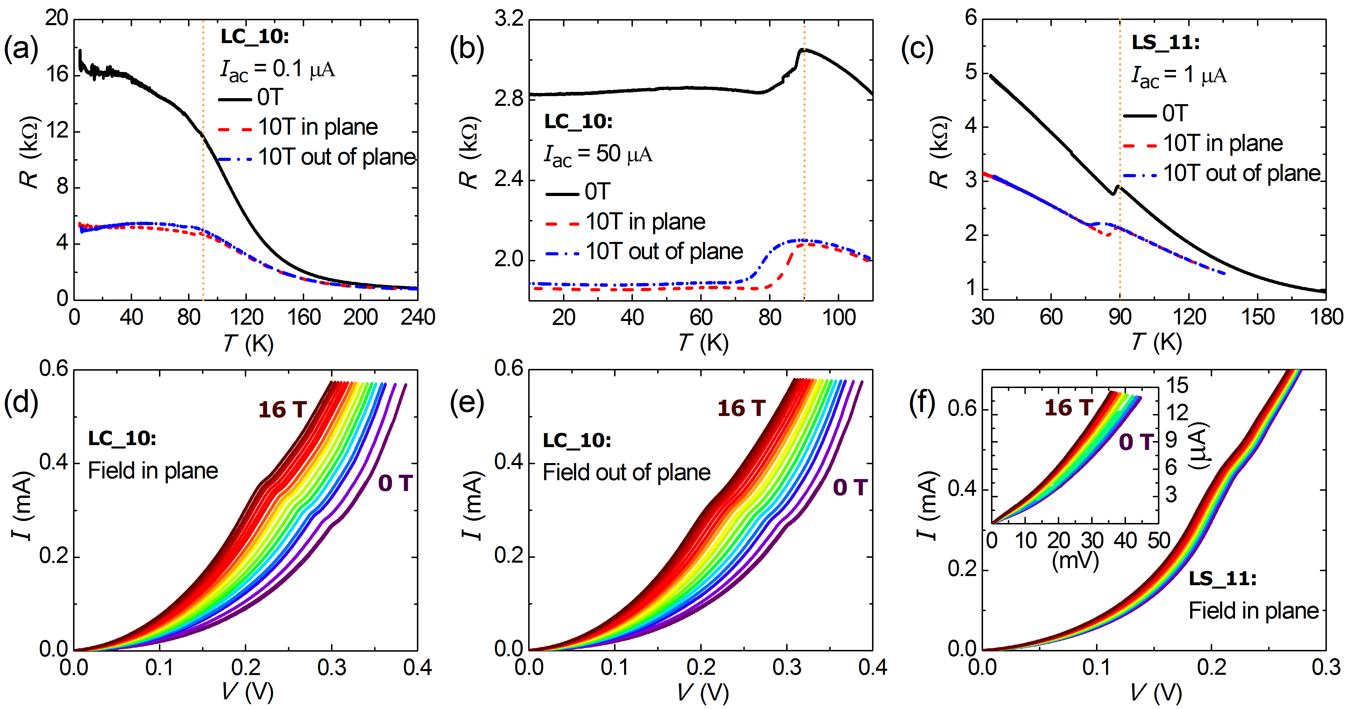
Figure 2 summarizes the vs. measurements and the current-voltage characteristics (-’s) at the base temperature of 7 K in different magnetic fields, obtained from the junctions made on LC_10 and LS_11 trilayers. Figure 2 (a) shows representative curves as measured with a small ac-bias current of A for junction No. 2 of LC_10 at zero field (black line) and at 10 T for in-plane (red line) and out-of-plane (blue line) orientation. A SEM picture of this junction is shown in Fig. 1 (a).
It is evident that the junction has a much higher resistance than the bridge, see Fig. 1 (f), and displays an insulating dependence. Furthermore, it exhibits a large negative magnetoresistance (MR), characteristic of the CMR effect of the manganites, that appears below K, increases rapidly below K and is almost isotropic with respect to the field orientation. These data suggest that the thin LCMO layer behaves as a ferromagnetic insulator (FI) with a small band-gap, qualitatively similar to the LaMnO3+δ layers of the previously studied junctions of Refs. Golod_2013; Roberto_2019. From Fig. 2 (a) it can also be seen that the low-bias does not drop at and continues to increase with decreasing temperature. Therefore, at this low bias, there is no supercurrent passing through the 10 nm thick FI layer. This indicates that the LCMO layer is uniform (without microshots) and that there is no direct tunneling of Cooper pairs through the LCMO barrier.
Fig. 2 (b) shows for the same junction measured at a 500 times larger ac-current of A. At this high bias signatures of the superconducting transition are clearly seen, although the resistance does not drop to zero. Fig. 2 (c) shows a similar behavior for the junction with the LSMO barrier measured at an intermediate current of A. This type of unusual superconducting proximity effect through a FI layer at large bias has been reported earlier for YBCO/LMO/YBCO junctions Golod_2013; Roberto_2019. It was attributed to the occurrence of a Zenner-type tunneling at a bias voltage larger than the band-gap of the FI and subsequent direct Cooper pair transport in the conduction band of the FI.
Figures 2 (d-f) display - curves measured in the superconducting state at K at different magnetic fields, ranging from 0 T to 16 T with field increments of 1 T. Panels (d) and (e) show the data for the junction on LC_10 with in-plane and out-of-plane fields, respectively, and (f) for the junction on LS_11 with in-plane fields. The reduction of the resistance with increasing field, due to the negative CMR, is once more clearly seen. Note that, in line with the above described bias dependence of the resistance, the - curves are strongly non-linear with a decrease in the differential resistance towards increasing bias. There is also a well-defined kink in the - curves which in zero magnetic field occurs at V for LCMO and V for LSMO. Such a kink was also observed for the YBCO/LMO/YBCO junctions in Ref. Golod_2013 and explained in terms of Zenner tunneling, leading to an anomalous high-bias proximity effect through the conduction band of the ferromagnetic insulator. Notably, the kink voltage in the -’s of the junctions with the LCMO and LSMO barriers, see Figs. 2 (d-f), has a 4-5 times smaller value than for the junctions with the LMO barrier Golod_2013; Roberto_2019. This trend is qualitatively consistent with the expectation that the band gaps of LCMO and LSMO, which should be both very close to a half-metallic state, are considerably smaller than the one of the ferromagnetic insulator LMO. Note that the weak insulator-like behavior of the LCMO and LSMO layers (which in the bulk are half-metallic) can be understood in terms of the strain and disorder effects, which are common for such thin layers as well as a charge transfer at the interface between the manganite and YBCO Varela_2003; Chakhalian2007; Holden_2004.
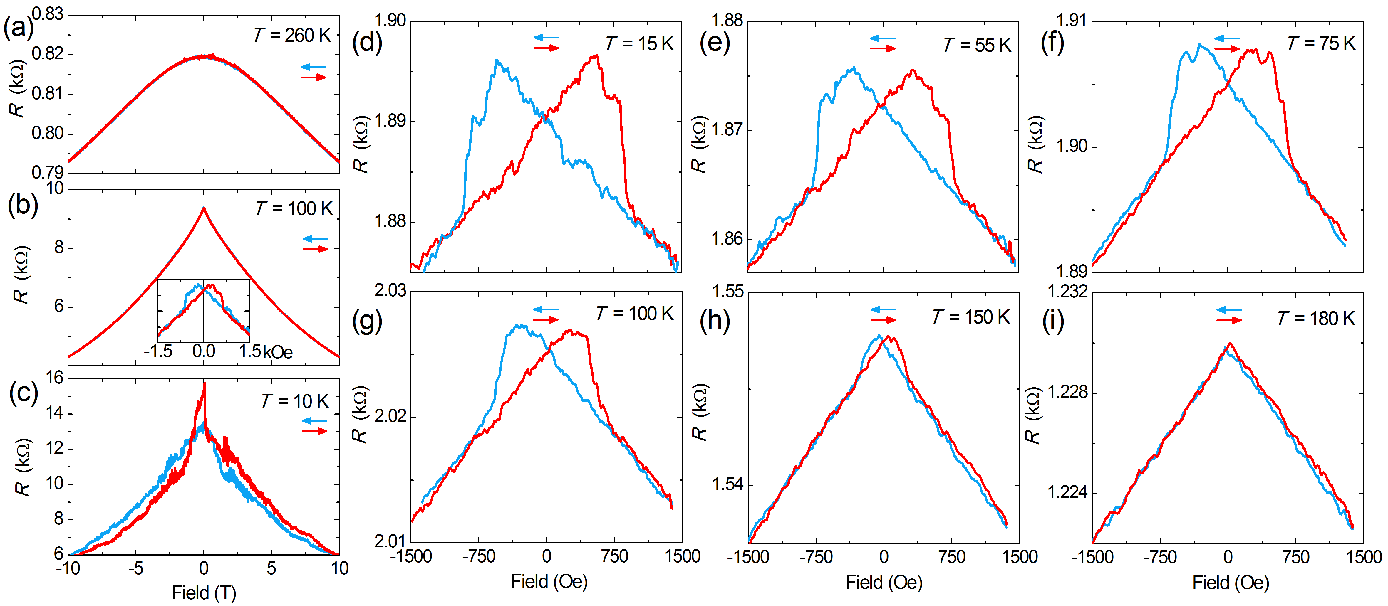
Figure 3 shows the magneto-resistance (MR) curves for junction No. 2 of LC_10 at different temperatures for an in-plane magnetic field. Panels (a-c) show the MR curves for a small ac current of A over a large field ranging from -10 T to +10 T at representative temperatures of (a) K, (b) K and (c) K . A negative MR, typical for the CMR manganites, occurs in the entire temperature range. Above K of the LCMO layer, see Fig. 3 (a), the MR is relatively small and the curve has a smooth shape with a broad maximum at zero field that does not exhibit any hysteresis with respect to the direction of the field sweeping. Below the CMR effect becomes rather large with a maximal value of at 10 T at low . As shown in the inset of Fig. 3 (b), the curves exhibit now clear hysteretic effects around the origin that are indicative of a field-induced magnetization switching of ferromagnetic domains at a finite coercive field .
Additional hysteresis effects and irregularities in the MR curves that appear below are likely related to Abrikosov vortices that enter the superconducting YBCO electrodes, see Fig. 3 (c). The stray fields from these vortices can lead to large offset fields in the FM barrier (on the order of kOe per vortex Golod_2015). The vortex pinning thus can strongly affect the hysteresis and the shape of the measured MR curves. These vortex-induced effects can be avoided if the sweep range is limited to small enough fields for which the vortex cannot enter the sample. An estimate of this vortex entrance field can be obtained by dividing the flux quantum by the cross sectional area of the electrode, which for our junctions amounts to kOe thanks to the small crossection area ( nm2) for the in-plane field orientation, see Fig. 1 (c). The vortex entrance field is further increased by the mesoscopic nature of our junctions with an electrode size that is comparable to the London penetration depth of YBCO of nm. Moreover, the metastability of the vortex state can be reduced by applying a larger transport current.
Accordingly, Figures 3 (d)-(i) show MR-curves for different temperatures in a narrower field range measured with a larger ac current of 100 A. The hysteresis between the MR curve for upward (red) and downward (blue lines) field sweeps is now evident, and the curves are regular and very reproducible even below . All the MR loops exhibit a qualitatively similar behavior. Upon decreasing the field, when going from positive to negative field, increases linearly up to a maximum at a small negative field at which the resistance decreases abruptly, and in the following decreases linearly with the same absolute value of the slope as on the positive side. This hysteresis is most pronounced at low temperature, and its magnitude decreases continuously with increasing temperature without a clear disruption at . This behavior is qualitatively different from the magnetoresistance of superconducting films induced by stray fields from ferromagnets in S/F hybrid films Flokstra_2010. Therefore, the observed hysteresis on the MR loops is not related to vortices or superconductivity in YBCO, but is solely associated with the CMR of LCMO and reflects the switching of magnetization in the F-layer. This is fully consistent with our earlier conclusion that the resistance of the junction is almost entirely determined by the highly-resistive manganite interlayer in the ferromagnetic insulator state, compare resistances in Figs. 1 (f) and 2 (a). The observation of such magneto-resistive hysteresis loops in junctions with a single manganite layer is our central result.
The above described hysteresis of the MR curves has a fairly straightforward interpretation. The MR of the manganites depends on the absolute value of the magnetic induction , where and is the magnetization of the manganite layer. At high fields the ferromagnetic manganite layer is fully magnetized and reaches the saturation value . Upon decreasing the applied field (from positive to negative values) increases due to CMR effect for which . The curve exhibits a constant linear slope as long as the manganite layer remains fully saturated. This changes only close to the negative coercive field at which the magnetization flips to . Such a magnetization flipping causes a co-aligned orientation of and which leads to an increase of the magnetic induction and a corresponding decrease of . The abrupt decrease of at the corrective field thus reflects a sudden flipping of the magnetization of the ferromagnetic manganite layer. In general, the type of switching depends on the size and geometry of the F nano-particle. We observe in most cases an abrupt change of around that is typical for the switching of a barrier with a mono-(or few)-domain ferromagnetic state along the easy axis of magnetization. This type of switching is expected for an elongated nano-sized ferromagnetic layer for which the field is oriented parallel to the long axis, as occurs in our experiment (see Fig. 1 (c)).
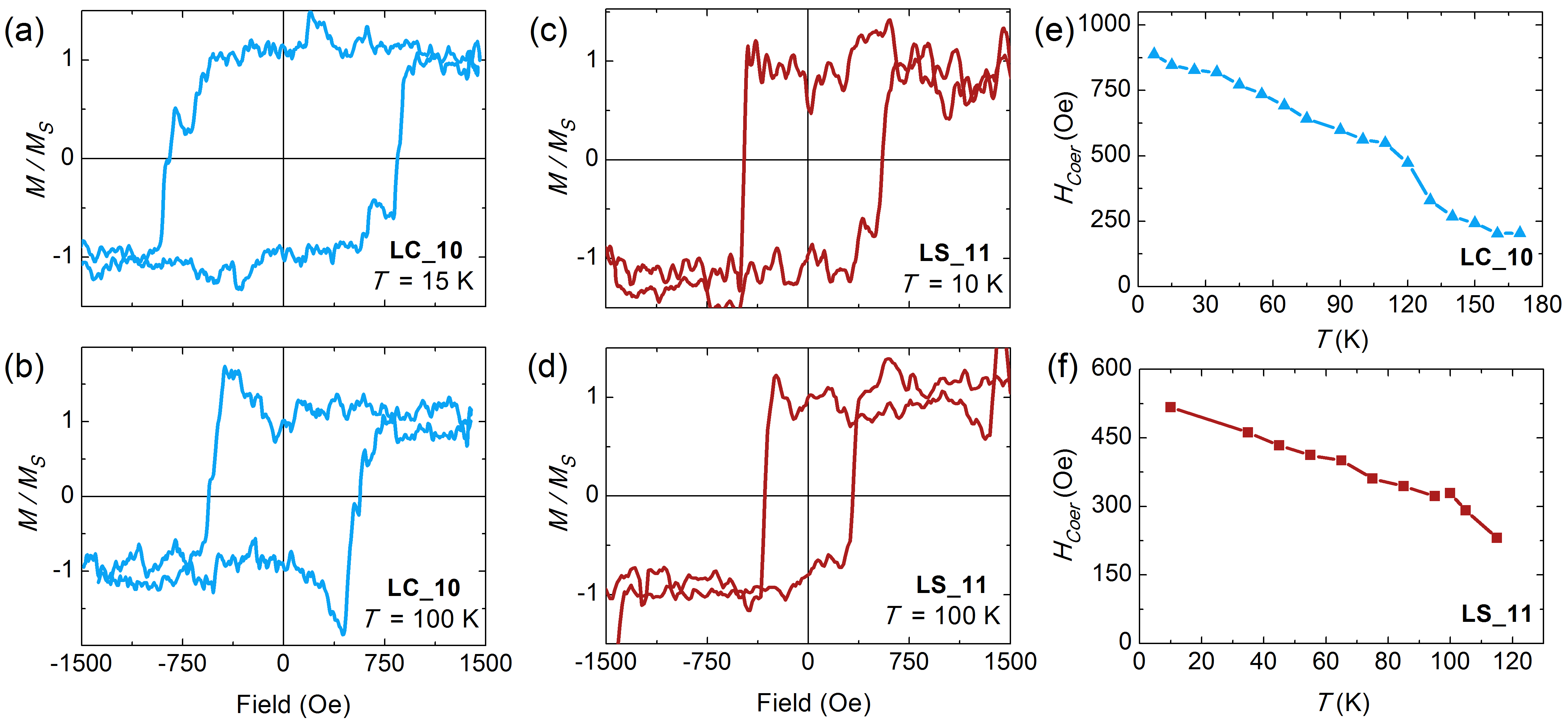
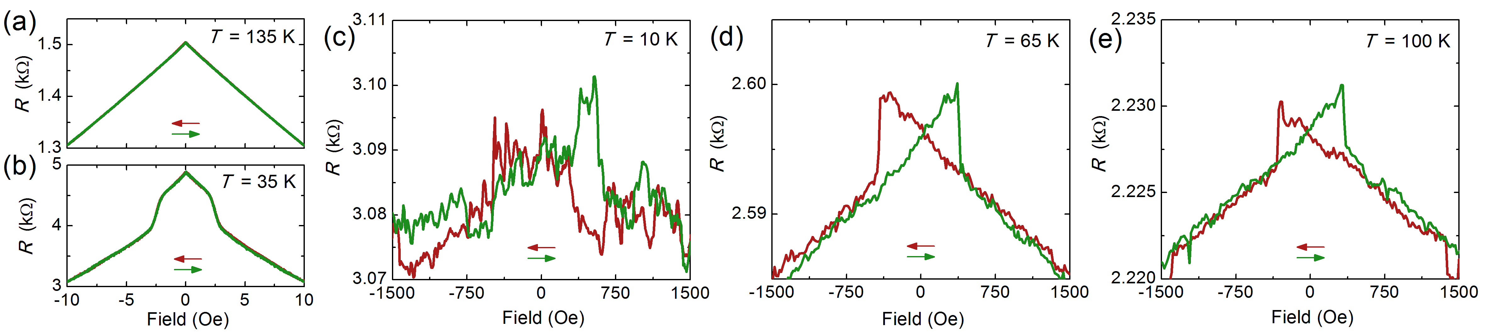
Figure 4 shows MR loops recorded from junction No. 2 on the YBCO/LSMO/YBCO trilayer. Figures 4 (a) and (b) show curves in a large field range of T, measured at A at temperatures (a) above and (b) below . A linear negative MR due to CMR in the LSMO layer is evident in panel (a). However, below we also observe a jump in the resistance around 3 T. This jump disappears as the measurement current is increased (not shown). Figures 4 (c-e) display corresponding MR-loops in a narrow field range, measured at a larger current of A, for the same junction. The overall behavior concerning the hysteresis is similar to the one of the junction with the LCMO barrier in Fig. 3. A closer comparison of the MR loops obtained from the junctions on LCMO and LSMO (Figs. 3 and 4) shows that the magnetic switching of the LSMO interlayer is abrupt and does not show any intermediate steps, while for LCMO a small intermediate step can be observed in some curves, see e.g. Fig. 3 (d). The latter may indicate the formation of two magnetic domains in the longer nm LCMO junction, while the shorter nm LSMO junction switches in a mono-domain manner. This is in line with the expected size and geometry dependencies of domain configurations in ferromagnetic nano-particles.
All together, the experimental data are consistent with the interpretation that the observed hysteretic MR loops of the junctions are due to a combination of ferromagnetic moment switching and CMR of the manganite barrier. The hysteresis arises from the finite coercive field for the remagnetization of the junction interlayer, while the CMR effect enables a resistive read-out of the direction of magnetization. This facilitates a memory operation of the junction with just one F-layer, as discussed below.
The simple linear MR (in a limited field range) allows us to reconstruct the in situ magnetization loop of the manganite nanoparticle forming the junction interlayer. The MR can be written as
| (1) |
where and is a constant coefficient. Thus,
| (2) |
The magnetization can be obtained as where the appropriate sign of needs to be chosen.
Figures 5 (a)-(d) show the magnetization loops that have been reconstructed from the MR loops in Figs. 3(d), 3(g), 4(c) and 4(e), for (a,b) the LCMO and (c,d) the LSMO interlayers. Panels (a) and (c) show the loops at low with superconducting YBCO electrodes, and panels (b) and (d) the ones at K for which YBCO is in the normal state. The magnetization loops have a rectangular shape and exhibit an abrupt switching behavior between the saturated magnetization states. The overall behavior is typical for a mono-domain switching along the easy axis, as expected for ferromagnetic nanoparticles with the applied field parallel to the longer side. This type of switching is sustained over a broad temperature range up to . The persistence of this magnetic switching behavior to high temperature is also seen in Figures 5 (e) and (f), which display temperature dependencies of the coercive fields for the two junctions, deduced from the reconstructed magnetization loops. Apparently, manganite nano-particles forming junction interlayers are acting as homogeneous (mono-domain type) CMR ferromagnets.
IV Memory functionality
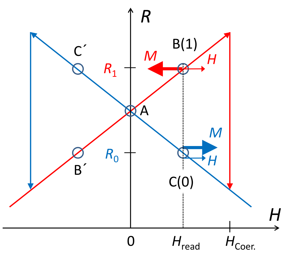
The combination of ferromagnetism and colossal magnetoresistance provides a unique memory functionality in our junctions with just a single F-layer. Figure 6 represents a sketch of the operation of such a CMR-based memory cell, which is based on the experimental MR-loops of Fig. 3. The memory information is stored, as usual, in terms of the orientation of the magnetization of the interlayer ferromagnetic nanoparticle. For example, in Fig. 6 we interpret the state with the magnetization pointing to the left and to the right as 1 and 0, respectively. The key requirement here is the switching of the ferromagnetic nanoparticle, which facilitates only two stable states with . This requirement is fulfilled in our junctions, as demonstrated in Fig. 5.
The resistance of the junction is determined by the magnetic induction , according to Eq. (1). Without an applied field at , point in Fig. 6, the two states are degenerate. This degeneracy is lifted if a local read-out magnetic field is applied, which should be smaller than the coercive field . Due to the CMR phenomenon, the resistance of the 1-state, point-, with opposite directions of and , , is larger than the resistance of the 0-state, point-, with co-aligned and , . The resistance change during the readout is or . A significant readout signal is facilitated here by the large CMR coefficient . The readout signal can be doubled by sequential measurements at opposite readout fields, as marked by points and in Fig. 6. This increases the readout fidelity and reduces the required readout field.
For a multi-bit random-access memory application the read-out field has to be local and individual for each cell, to avoid cross-talking. This may seem like a difficult task. However, instead of making a complex network of control lines, it is possible to utilize a self-field effect from the bias (read-out) current for the generation of the local field at the junction. Such a self-field phenomenon is well known and often utilized in superconducting Josephson-junctions Krasnov_1997; Golod_2019. Furthermore, the Meissner effect in superconductors leads to a so called “short-circuit principle” in a system of current-carrying superconducting electrodes. According to this principle, the current induced magnetic field is localized and enhanced between electrodes and does not affect the surroundings, as if the electrodes were short-circuited. With a proper design of bias electrodes, this may greatly reduce the cross-talking between neighboring memory cells.
Finally, we list the benefits of the proposed complex oxide YBCO/CMR-manganite/YBCO memory cells:
i) Extreme simplicity. Only a single F-layer is required for the operation of the memory cell.
ii) Non-volatility.
iii) Scalability to nm-sizes. The manganites preserve their ferromagnetic properties down to a size of about nm Roberto_2019. Such a miniaturization would require metallic manganites to reduce the junction resistance.
iv) High- superconductivity of YBCO allows comfortable operation at liquid nitrogen temperature. Zero resistance of electrodes enables low power dissipation and high operation speed.
v) The colossal magnetoresistance facilitates a large readout signal.
vi) The CMR readout does not rely on superconductivity. Therefore, such a memory cell can be operated even at room temperature for manganites like LSMO with K.
V Conclusions
To conclude, we have fabricated complex oxide Superconductor/Ferromagnet/Superconductor junctions with layers of the high- cuprate superconductor YBa2Cu3O7-x and the colossal magneto-resistive manganites La2/3X1/3MnO3+δ (X: Ca or Sr). Nano-scale YBCO/LCMO/YBCO and YBCO/LSMO/YBCO junctions with a minimum feature size down to nm have been fabricated and studied experimentally. We found that the LCMO and LSMO layers of these junctions are qualitatively similar and behave as ferromagnetic insulators with Curie temperatures of about 210 K for LCMO and above 300 K for LSMO. Therefore the junction characteristics, especially in the superconducting state of YBCO, carry solely information about the perpendicular transport properties of the manganite interlayers.
Our main new experimental result is the observation of hysteretic magneto-resistance loops, which are caused by the CMR effect in the manganite interlayer and, therefore, persist both below and above the superconducting critical temperature K. The shape of the MR loops reflects the shape of ferromagnetic magnetization loops. This allows for an in situ reconstruction of the magnetization loops of the ferromagnetic nanoparticle that forms the junction interface. The magnetization loops have rectangular shapes with abrupt switching between the saturated magnetization states, and are characteristic of a mono (or dual) domain switching of the ferromagnetic interlayer.
Finally, we have argued that the combination of a ferromagnetic response and a colossal magneto-resistance effect in our junctions facilitates a memory functionality. In such a S-CMR-S memory cell the information is stored in the orientation of the magnetization of a single F-layer, which can be read out at a finite magnetic field via the CMR effect. The main benefits of such a memory cell are an extreme simplicity with only a single F-layer; non-volatility; scalability to nm-sizes; high- superconductivity of YBCO which allows comfortable operation at liquid nitrogen temperature, low power dissipation and high operation speed; the CMR facilitates large readout signals (or small readout fields); furthermore, since the CMR readout does not rely on superconductivity, such a memory cell can operate even at room temperature. We have argued that such a device can be one of the elements of complex oxide electronics in general, and for a digital superconducting computer operating at liquid nitrogen, in particular.
Acknowledgements.
The work at the University of Fribourg was supported by the Swiss National Science Foundation (SNF) through grants No. 200020-172611 and CRSII2-154410/1. The work at SU is partly supported by the European Union H2020- WIDESPREAD- 05-2017-Twinning project SPINTECH under Grant Agreement No. 810144. V. M. K. is grateful for the hospitality during a visiting professor semester at MIPT, supported by the Russian Ministry of Education and Science within the program 5top100.References
- (1)