Tuning insulator-semimetal transitions in 3D topological insulator thin films by inter-surface hybridization and in-plane magnetic fields
Abstract
A pair of Dirac points (analogous to a vortex-antivortex pair) associated with opposite topological numbers (with Berry phases) can be merged together through parameter tuning and annihilated to gap the Dirac spectrum, offering a canonical example of a topological phase transition. Here, we report transport studies on thin films of BiSbTeSe2 (BSTS), which is a 3D TI that hosts spin-helical gapless (semi-metallic) Dirac fermion surface states (SS) for sufficiently thick samples, with an observed resistivity close to at the charge neutral point. When the sample thickness is reduced to 10 nm thick, the Dirac cones from the top and bottom surfaces can hybridize (analogous to a “merging” in the real space) and become gapped to give a trivial insulator. Furthermore, we observe that an in-plane magnetic field can drive the system again towards a metallic behavior, with a prominent negative magnetoresistance (MR, up to 95%) and a temperature-insensitive resistivity close to at the charge neutral point. The observation is interpreted in terms of a predicted effect of an in-plane magnetic field to reduce the hybridization gap (which, if small enough, may be smeared by disorder and a metallic behavior). A sufficiently strong magnetic field is predicted to restore and split again the Dirac points in the momentum space, inducing a distinct 2D topological semimetal (TSM) phase with 2 single-fold Dirac cones of opposite spin-momentum windings.
A wide range of quantum materials including graphene, topological insulators (TIs), Dirac/Weyl semimetals, and their artificial analogues, have been identified whose low-energy excitations behave as massless Dirac particles to host novel relativistic quantum phenomena Castro Neto et al. (2009); Hasan and Kane (2010); Qi and Zhang (2011); Armitage et al. (2018); Lu et al. (2014); Bellec et al. (2013); Tarruell et al. (2012). The Dirac spectra can be gapped by breaking the underlying symmetry that protects the Dirac points (DPs), or by pairwise merging and annihilation of DPs Bellec et al. (2013); Tarruell et al. (2012); Wehling et al. (2014); Hasegawa et al. (2006); Baik et al. (2015); Pereira et al. (2009); Feilhauer et al. (2015). Previously predicted material platforms to explore this latter mechanism, such as graphene with engineered anisotropic nearest-neighbor hopping Hasegawa et al. (2006) and thin black phosphorus under a strong electric field Baik et al. (2015), require extreme parameter tuning that is difficult to realize experimentally Pereira et al. (2009); Feilhauer et al. (2015); Kim et al. (2015). Alternative platforms that have enabled experimental demonstration of this effect include a microwave analogue of strained graphene Bellec et al. (2013) and cold atoms in honeycomb optical lattices Tarruell et al. (2012). On the other hand, 3D TI thin films with hybridization gapped surface states bring new opportunities to study such topological transitions in a solid-state system. In particular, merging and annihilating of top and bottom surface DPs (with opposite spin windings) can be controlled both in the real space (by sample thickness, for example demonstrated experimentally in Ref. Zhang et al. (2010) by angle-resolved photoemission spectroscopy on thin films grown by molecular beam epitaxy) and the momentum space (by an in-plane magnetic field, as theoretically proposed in Ref. Zyuzin et al. (2011)).
In a relatively thick 3D TI film (thickness nm), the top and bottom surfaces are well separated and their corresponding topological SS Dirac cones are gapless with opposite spin helicities. When the sample is thin enough (typically 10 nm) to enable hybridization between the two surfaces, a gap is opened at the DP (even though the time-reversal symmetry is still preserved). The SS band structure acquires massive Dirac dispersion , with being the Plank constant divided by , the Fermi velocity and the (in-plane) wave vector Zhang et al. (2010). Such a crossover of 3D TIs to the two-dimensional (2D) limit, as well as their response to magnetic fields, is little explored by electronic transport measurements in 3D TI materials with no bulk conduction and surface-dominant transport (such as BSTS). Previous in-plane magneto-transport studies in 3D TIs often suffer from their residual bulk conduction Wiedmann et al. (2016); Breunig et al. (2017) and few have been reported in the hybridization regime Lin et al. (2013); Liao et al. (2015); Taskin et al. (2017).
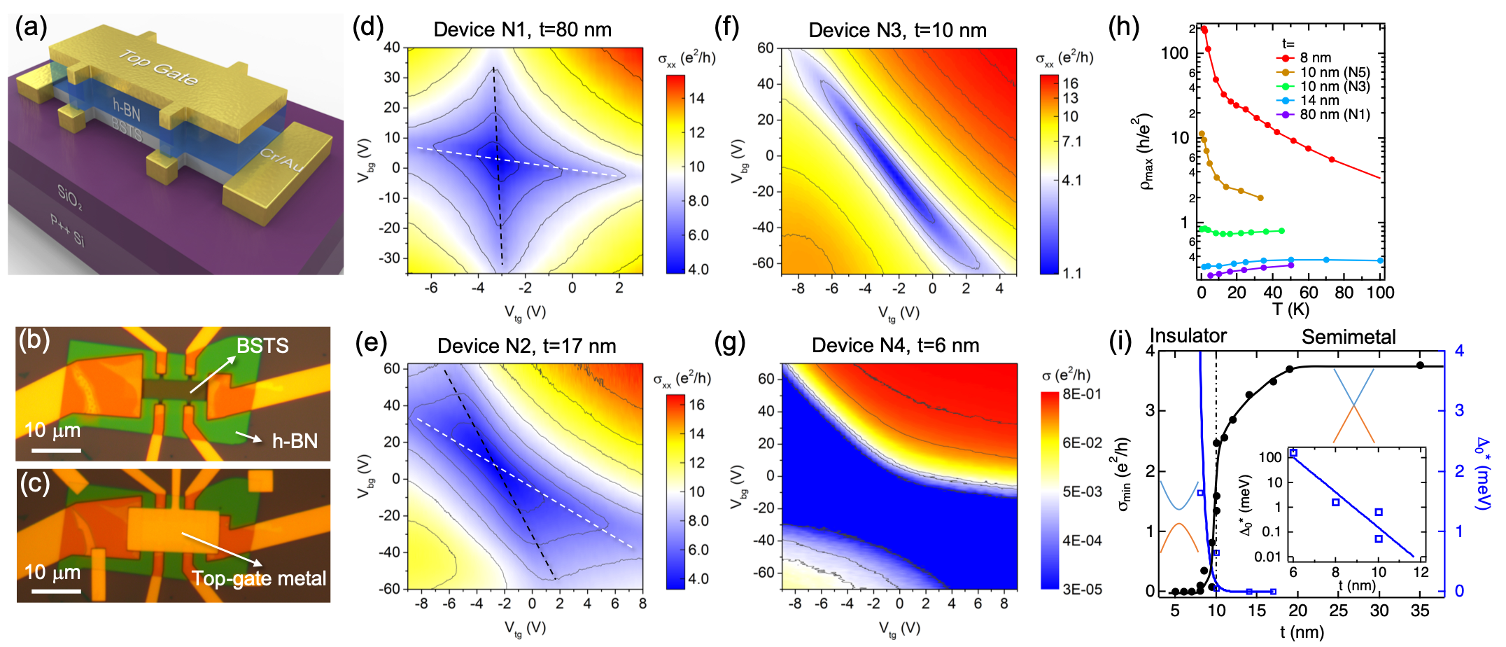
Our experiment is based on a 3D TI crystal BSTS (BiSbTeSe2) that has no detectable bulk conducting carriers at low temperature, with DPs of the topological SS exposed in the bulk band gap Xu et al. (2014, 2016), thus ideal for the study of low energy excitations in the vicinity of the surface DPs. The dual-gated BSTS devices Xu et al. (2016) were fabricated into Hall-bar structures (with channel length , width , thickness ) on highly p-doped Si substrates (with 300 nm-thick SiO2 coating). Hexagonal boron nitride (h-BN) flakes (tens of nm in thickness) are transferred onto the devices as top-gate dielectrics (see a typical device schematic in Fig. 1a and optical images of Device N3 in Fig. 1b, c). Top and back gate voltages (denoted as and ) relative to the BSTS flake are applied to the top-gate metal and the doped Si, respectively. Upon dual-gating, the carrier types and densities of both the top and bottom surfaces, thus the measured conductivity, can be modulated. By reducing the thickness of the BSTS flake, the capacitive coupling between the two surfaces becomes stronger Kim et al. (2012); Fatemi et al. (2014). As it can be seen in the color map of 2D conductivity (), with being the longitudinal resistance) versus and measured at low temperature, the black and white dashed lines tracing the DPs of top and bottom surfaces tend to merge together when the thickness t is reduced from 80 nm to 17 nm (Fig. 1d and 1e). Further reducing to 10 nm results in the DPs from the two surfaces to become indistinguishable (Fig. 1f). When the sample is only a few nm thick (e.g., Device N4 with nm in Fig. 1g), a hard gap opens, as indicated by the highly insulating (two-terminal conductivity ) blue region.
The minimum conductivity and maximum resistivity (=1/) are reached when the two surfaces are gated simultaneously to charge neutrality or DPs. In Fig. 1h, we plotted as a function of temperature () for a few representative samples. At nm, shows a metallic behavior (), implying a zero or negligible gap. However, at nm, a strong insulating behavior () is observed. Around nm, different samples can behave differently. For example, while device N5 exhibits an insulating behavior, another device N3 exhibits a non-monotonic temperature dependence with its close to and separating curves with metallic and insulating behaviors. It is consistent with the general observation from previous studies that the critical resistivity for metal-insulator transition in 2D electron systems is on the order of the resistance quantum Das Sarma and Hwang (2014). Fig. 1i shows at base temperatures ( K) for samples with various thicknesses. At large (20 nm), saturates around a value close to Xu et al. (2016). The starts to decrease below 20 nm and drops abruptly to zero below nm. For samples that exhibits insulating behaviors, their were fitted to thermal activation behavior (with being the Boltzmann constant) over appropriate temperature ranges to extract (see SI for details) the non-zero gap , plotted on the right axis of Fig. 1i. The grows by about an order of magnitude when is reduced by 1.4 nm (see the exponential fitting in the inset of Fig. 1i), comparable to what was found for Bi2Se3 Zhang et al. (2010); Kim et al. (2013). Our data suggest that a measurable transport gap (presumably driven by the inter-surface hybridization) opens at the DPs below a critical thickness nm in our samples.
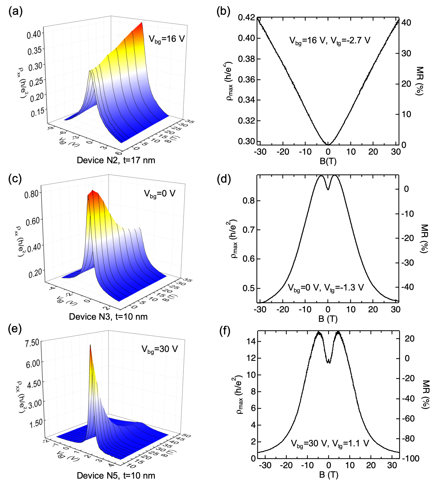
We have found that the resistances of the thicker and thinner samples respond to the in-plane magnetic field differently at low temperatures. For consistency, the samples are mounted with current direction parallel to (unless otherwise specified). We have measured multiple samples by either sweeping (with carefully tuned and then fixed at voltages such that these sweeps go through ) at different in-plane fields, or measuring versus in-plane at fixed gate voltages. For relatively thick samples such as Device N2 with nm, the in-plane field up to 31 T only induced a relatively small positive MR of 40% (Fig. 2a and 2b, noting is approximately proportional to at low fields and to at higher fields). At low fields ( T), thinner devices N3 and N5 (both 10 nm) also show some positive MR (for N5, we also observed an additional tiny cusp with negative MR near 0 T). Such low-field features in thinner devices disappear when we increase the temperature to just a few Kelvin (see SI), thus are attributed to phase coherent transport Lin et al. (2013); Liao et al. (2015). In the following, we mainly focus on the higher field data showing a giant negative MR that has only been observed in thin samples with insulating behavior (hybridization gapped). For example, in Device N3 (Fig. 2c and 2d), drops dramatically above 5 T and saturates at high field (30 T) to . Notably for the more insulating sample N5 (Fig. 2e and 2f), drops by a factor of 20 (giving an MR-95%) from a very resistive value of at T to a value () again close to at T. We have verified that Device N5 also showed a large negative MR (-85% at 31 T) when the in-plane field is perpendicular to the current direction (SI Fig. S6). This contrasts with the negative MR associated with chiral anomaly in 3D Dirac/Weyl semimetals Xiong et al. (2015) and with various scattering mechanisms Goswami et al. (2015); Wiedmann et al. (2016), as in those cases the negative MR disappears when the current is orthogonal to . The field and temperature dependences we observed, as further discussed below, are also different from the behavior due to quantum interference effect in a variable-range-hopping regime Sivan et al. (1988).
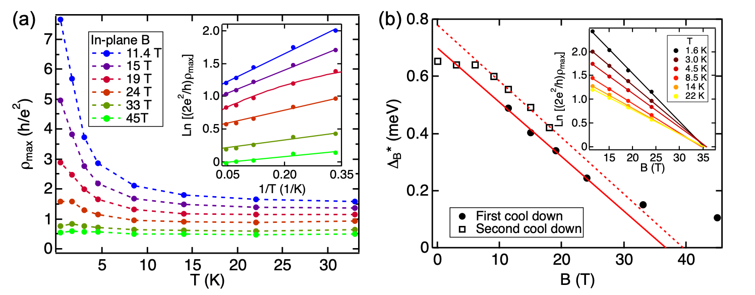
We performed systematic sweeps (fixed V) to extract with temperatures at various in-plane fields from 11.4 T to 45 T in Device N5. As shown in Fig. 3a, the insulating behavior of is strongly suppressed at higher fields. At the highest field (45 T), saturates to a value close to and becomes relatively insensitive to temperature. We estimated the thermal activation gap from the slope of Ln] versus in the temperature range of 3 K to 22 K (Fig. 3a inset) and plotted it versus the corresponding in Fig. 3b, which also displays the gap size measured in another (second) cool down for up to 18 T. The gap size is found to differ slightly over different cool-downs but exhibits a similar dependence on in the intermediate field range (5 T30 T).
Extrapolating the linear fits in Fig. 3b to zero suggests that the gap would close at a critical field () between 36 T to 40 T, around which we observe the sample (N5) to become metallic (, see Fig. 3a) below K. However, some non-metallic behavior () can still be observed between 2 K to 22 K even at the highest fields (Fig. 3a) and fitted to a thermal activation, giving data points that deviate from the red solid line (Fig. 3b). A non-metallic behavior under large in-plane magnetic fields was also observed in gapless samples such as N2 with nm (SI Fig. S8b). The reason for this behavior remains to be understood. We have also verified that Ln of sample N5 is linear with ( T) at different temperatures and all the fitted lines converge to a critical field of 36 T (inset of Fig. 3b). This also suggests , with a saturation resistivity (when ) and gap closing at 36 T at fixed temperatures.
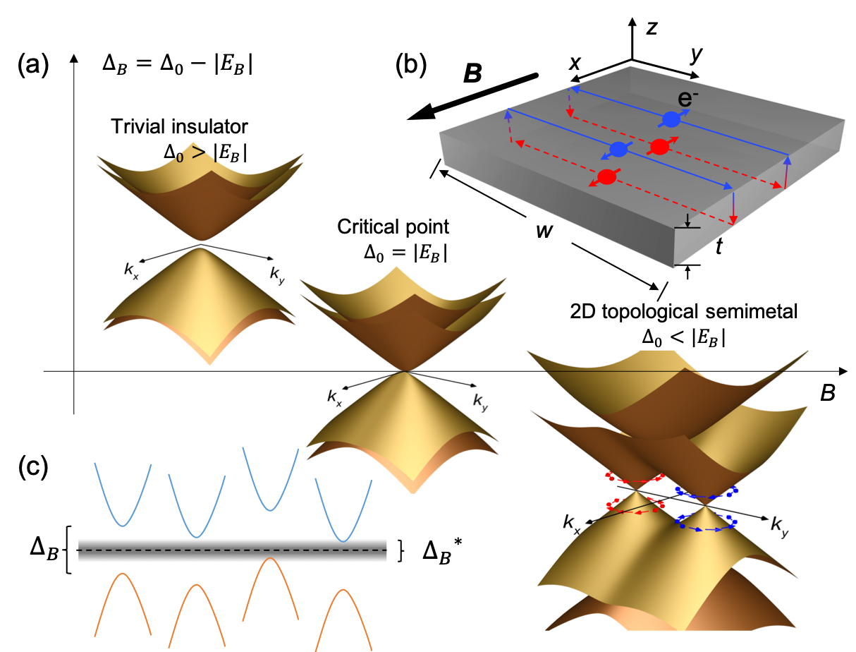
Such large negative MR and the corresponding insulator-semimetal transition have not been reported before in thin nonmagnetic 3D TIs with surface dominant conduction. Our observations of distinct behavior between thick and thin BSTS samples may be interpreted in terms of a theoretical prediction by A. A. Zyuzin et al. Zyuzin et al. (2011). Generally, in thick TIs the in-plane magnetic field (set to be along the direction) can introduce opposite shifts (along ) of top and bottom surface Dirac cones in the momentum space. This does not produce any MR effect in thick 3D TIs but will prevent the two DPs from annihilation and will tend to eliminate the hybridization gap in thin TIs (schematics shown in Fig. 4a). Semiclassically, a spin-helical SS electron with spin orientated along the field (thus spin magnetic moment , with being the in-plane spin g-factor and the Bohr magneton) moves clockwise around the circumference (Fig. 4b) with orbital magnetic moment (parallel to field) (noting width in our samples) Minot et al. (2004). Both the spin and orbital magnetic moments couple to the field, giving rise to an effective Zeeman energy (total effective , the second term can also be considered as due to the Aharonov-Bohm phase gradient between the two opposite surfaces). In thin TIs with hybridization gap (at zero field), one can show (Ref. Zyuzin et al. (2011) and SI) that the massive Dirac band is spin-split by the above “effective Zeeman energy”, shrinking the hybridization gap linearly with as . The gap vanishes at a critical field (), where the dispersion near becomes quadratic along and linear along (see Fig. 4a). With further increasing (), two DPs are restored and separated by along . This gives rise to a distinct 2D TSM that is topologically stable as long as translational symmetry is preserved Zyuzin et al. (2011).
The above mechanism can qualitatively explain the trend we observed in experiments. However, the slope of the linear fitting yields the gap closing rate meV/T (corresponding to ). This is nearly two orders of magnitudes smaller compared with meV/T theoretically estimated for a 10-nm sample by A. A. Zyuzin et al. Zyuzin et al. (2011), which assumed , leading to a negligibly small contribution from the Zeeman effect. Our results imply a large , giving rise to a Zeeman term () that is comparable with the orbital term (). Thus, the two nearly cancel to give a small . Assuming a typical m/s for topological SS with purely linear dispersion, we get a in-plane SS g-factor of . In actual 3D TI materials such as BSTS, the surface Dirac cone contains substantial nonlinearity that can be described by a quadratic mass term added to the SS Hamiltonian. Subsequently, a reduced m/s, which describes the linear part in the Hamiltonian, yields a g-factor of (SI). It has been pointed out that the Zeeman coupling of the SS carriers can be highly anisotropic Chu et al. (2011). In previous experiments, only an out-of-plane SS g-factor is determined and found to vary significantly in different TI materials Taskin and Ando (2011); Fu et al. (2016). Our study provides a method to extract the in-plane g-factor of SS carriers.
We have to note that in our experiments, the gap extracted from thermal activation is an effective transport gap () and can be smaller than the real band gap () due to disorder-induced smearing, namely , where is a correction due to the potential fluctuations (likely to be on the order of several meV or higher Nam et al. (2017)) in the system (Fig. 4c). Therefore, the observed apparent metallic behavior ( reaching 0) in Device N5 above 36 T does not necessarily indicate the realization of the 2D TSM phase, which requires closing the real gap and possibly much larger magnetic field than (noting the relatively small gap-closing rate of 0.02 meV/T in light of the estimated meV in our BSTS samples). It might be easier to realize the 2D TSM phase (at lower field) in other TI systems with a smaller or even negative g-factor (so the gap closing rate can be much larger than that in our samples). It would also be interesting for future studies to clarify whether the saturation resistivity is related to the modification of band structure and magnetic field induced spin-flip scatterings Taskin et al. (2017).
To summarize, we have demonstrated in ultrathin BSTS films with hybridized and gapped surface states a transition from an insulator to semimetal induced by either increasing thickness or an in-plane magnetic field. The in-plane magnetic field can shrink the hybridization gap and give a large negative MR that may be exploited for applications. Sufficient in-plane magnetic field is predicted to drive the thin 3D TI with hybridization gap to a 2D TSM phase, which would have 2 single-fold Dirac cones separated in the momentum space and provide a 2D analogue of Weyl semimetal (even though Weyl fermions cannot be strictly defined in even spatial dimensions Armitage et al. (2018)). Such a TSM (with the momentum space displacement between Dirac cones tunable by the in-plane magnetic field) can possess interesting 1D edge states Castro Neto et al. (2009); Takahashi (2015), which are analogous to the Fermi arcs in 3D Weyl semimetals Armitage et al. (2018) and have signatures that future experiments (e.g. performed at even higher magnetic fields) can search as evidence for the TSMs.
Acknowledgements.
We thank A. Suslov, T. Murphy, J-H. Park and Z. Lu for experimental assistance, and Y. Jiang, C. Liu and K. T. Law for discussions. This work has benefited from partial support from DARPA MESO program (Grant N66001-11-1-4107) and NSF (Grant DMR #1410942 and EFMA #1641101). G. Jiang and R. Biswas were supported by Purdue University startup funds. A portion of this work was performed at the National High Magnetic Field Laboratory, which is supported by NSF Cooperative Agreement No. DMR-1157490, the State of Florida, and the U.S. Department of Energy.References
- Castro Neto et al. (2009) A. H. Castro Neto, F. Guinea, N. M. R. Peres, K. S. Novoselov, and A. K. Geim, Reviews of Modern Physics 81, 109 (2009).
- Hasan and Kane (2010) M. Z. Hasan and C. L. Kane, Reviews of Modern Physics 82, 3045 (2010).
- Qi and Zhang (2011) X.-L. Qi and S.-C. Zhang, Reviews of Modern Physics 83, 1057 (2011).
- Armitage et al. (2018) N. P. Armitage, E. J. Mele, and A. Vishwanath, Reviews of Modern Physics 90, 015001 (2018).
- Lu et al. (2014) L. Lu, J. D. Joannopoulos, and M. Soljačić, Nature Photonics 8, 821 (2014).
- Bellec et al. (2013) M. Bellec, U. Kuhl, G. Montambaux, and F. Mortessagne, Physical Review Letters 110, 033902 (2013).
- Tarruell et al. (2012) L. Tarruell, D. Greif, T. Uehlinger, G. Jotzu, and T. Esslinger, Nature 483, 302 (2012).
- Wehling et al. (2014) T. Wehling, A. Black-Schaffer, and A. Balatsky, Advances in Physics 63, 1 (2014).
- Hasegawa et al. (2006) Y. Hasegawa, R. Konno, H. Nakano, and M. Kohmoto, Physical Review B 74, 033413 (2006).
- Baik et al. (2015) S. S. Baik, K. S. Kim, Y. Yi, and H. J. Choi, Nano Letters 15, 7788 (2015).
- Pereira et al. (2009) V. M. Pereira, A. H. Castro Neto, and N. M. R. Peres, Physical Review B 80, 045401 (2009).
- Feilhauer et al. (2015) J. Feilhauer, W. Apel, and L. Schweitzer, Physical Review B 92, 245424 (2015).
- Kim et al. (2015) J. Kim, S. S. Baik, S. H. Ryu, Y. Sohn, S. Park, B.-G. Park, J. Denlinger, Y. Yi, H. J. Choi, and K. S. Kim, Science 349, 723 (2015).
- Zhang et al. (2010) Y. Zhang, K. He, C.-Z. Chang, C.-L. Song, L.-L. Wang, X. Chen, J.-F. Jia, Z. Fang, X. Dai, W.-Y. Shan, S.-Q. Shen, Q. Niu, X.-L. Qi, S.-C. Zhang, X.-C. Ma, and Q.-K. Xue, Nature Physics 6, 584 (2010).
- Zyuzin et al. (2011) A. A. Zyuzin, M. D. Hook, and A. A. Burkov, Physical Review B 83, 245428 (2011).
- Wiedmann et al. (2016) S. Wiedmann, A. Jost, B. Fauqué, J. van Dijk, M. J. Meijer, T. Khouri, S. Pezzini, S. Grauer, S. Schreyeck, C. Brüne, H. Buhmann, L. W. Molenkamp, and N. E. Hussey, Physical Review B 94, 081302(R) (2016).
- Breunig et al. (2017) O. Breunig, Z. Wang, A. A. Taskin, J. Lux, A. Rosch, and Y. Ando, Nature Communications 8, 15545 (2017), 1703.10784 .
- Lin et al. (2013) C. J. Lin, X. Y. He, J. Liao, X. X. Wang, V. Sacksteder IV, W. M. Yang, T. Guan, Q. M. Zhang, L. Gu, G. Y. Zhang, C. G. Zeng, X. Dai, K. H. Wu, and Y. Q. Li, Physical Review B 88, 041307(R) (2013).
- Liao et al. (2015) J. Liao, Y. Ou, X. Feng, S. Yang, C. Lin, W. Yang, K. Wu, K. He, X. Ma, Q. K. Xue, and Y. Li, Physical Review Letters 114, 216601 (2015).
- Taskin et al. (2017) A. A. Taskin, H. F. Legg, F. Yang, S. Sasaki, Y. Kanai, K. Matsumoto, A. Rosch, and Y. Ando, Nature Communications 8, 1340 (2017).
- Xu et al. (2014) Y. Xu, I. Miotkowski, C. Liu, J. Tian, H. Nam, N. Alidoust, J. Hu, C.-K. Shih, M. Z. Hasan, and Y. P. Chen, Nature Physics 10, 956 (2014).
- Xu et al. (2016) Y. Xu, I. Miotkowski, and Y. P. Chen, Nature Communications 7, 11434 (2016).
- Kim et al. (2012) D. Kim, S. Cho, N. P. Butch, P. Syers, K. Kirshenbaum, S. Adam, J. Paglione, and M. S. Fuhrer, Nature Physics 8, 460 (2012).
- Fatemi et al. (2014) V. Fatemi, B. Hunt, H. Steinberg, S. L. Eltinge, F. Mahmood, N. P. Butch, K. Watanabe, T. Taniguchi, N. Gedik, R. C. Ashoori, and P. Jarillo-Herrero, Physical Review Letters 113, 206801 (2014).
- Das Sarma and Hwang (2014) S. Das Sarma and E. H. Hwang, Physical Review B 89, 235423 (2014).
- Kim et al. (2013) D. Kim, P. Syers, N. P. Butch, J. Paglione, and M. S. Fuhrer, Nature Communications 4, 2040 (2013).
- Xiong et al. (2015) J. Xiong, S. K. Kushwaha, T. Liang, J. W. Krizan, M. Hirschberger, W. Wang, R. J. Cava, and N. P. Ong, Science 350, 413 (2015).
- Goswami et al. (2015) P. Goswami, J. H. Pixley, and S. Das Sarma, Physical Review B 92, 075205 (2015).
- Sivan et al. (1988) U. Sivan, O. Entin-Wohlman, and Y. Imry, Phys. Rev. Lett. 60, 1566 (1988).
- Minot et al. (2004) E. D. Minot, Y. Yaish, V. Sazonova, and P. L. McEuen, Nature 428, 536 (2004).
- Chu et al. (2011) R.-L. Chu, J. Shi, and S.-Q. Shen, Physical Review B 84, 085312 (2011).
- Taskin and Ando (2011) A. A. Taskin and Y. Ando, Physical Review B 84, 035301 (2011).
- Fu et al. (2016) Y.-S. Fu, T. Hanaguri, K. Igarashi, M. Kawamura, M. S. Bahramy, and T. Sasagawa, Nature Communications 7, 10829 (2016).
- Nam et al. (2017) H. Nam, Y. Xu, I. Miotkowski, J. Tian, Y. P. Chen, C. Liu, M. Z. Hasan, W. Zhu, G. A. Fiete, and C.-K. Shih, Journal of Physics and Chemistry of Solids (2017), doi:10.1016/j.jpcs.2017.10.026.
- Takahashi (2015) R. Takahashi, in Topological States on Interfaces Protected by Symmetry (Springer Japan, Tokyo, 2015) pp. 63–71.
![[Uncaptioned image]](/html/1904.03722/assets/x1.png)
![[Uncaptioned image]](/html/1904.03722/assets/x2.png)
![[Uncaptioned image]](/html/1904.03722/assets/x3.png)
![[Uncaptioned image]](/html/1904.03722/assets/x5.png)
![[Uncaptioned image]](/html/1904.03722/assets/x6.png)
![[Uncaptioned image]](/html/1904.03722/assets/x7.png)
![[Uncaptioned image]](/html/1904.03722/assets/x8.png)
![[Uncaptioned image]](/html/1904.03722/assets/x9.png)
![[Uncaptioned image]](/html/1904.03722/assets/x10.png)
![[Uncaptioned image]](/html/1904.03722/assets/x11.png)
![[Uncaptioned image]](/html/1904.03722/assets/x12.png)
![[Uncaptioned image]](/html/1904.03722/assets/x13.png)