Grain boundary characteristics of oxypnictide NdFeAs(O,F) superconductors
Abstract
We have systematically investigated the grain boundary angle () dependence of transport properties for NdFeAs(O,F) fabricated on [001]-tilt symmetric MgO bicrystal substrates. In our previous study, NdFeAs(O,F) bicrystal films showed a weak-link behaviour even at a of 6∘. However, this was caused by an extrinsic effect originating from the damage to both NdFeAs(O,F) and MgO substrate by excess F-diffusion along the grain boundary. To investigate the intrinsic nature of grain boundaries, we minimized the damage to NdFeAs(O,F) and MgO by reducing the deposition temperature of NdOF over-layer needed for F-doping. The resultant NdFeAs(O,F) bicrystal films have a critical angle of 8.5∘, above which starts to decrease exponentially. This critical angle is almost the same as those of other Fe-based superconductors.
1 Introduction
The discovery of iron-based superconductors (FBS) triggered a huge excitement for the community of fundamental and applied superconductivity research. Since then many physical quantities of FBS have been revealed, e.g. the coherence length is short, which results from the small Fermi velocity and low carrier density [1]. The in-plane coherence length at zero kelvin obtained from upper critical field measurements is 24 nm for FBS [e.g. the respective for Fe(Se,Te), BaFe2(As0.7As0.3)2, (Ba,K)Fe2As2, NdFeAsO0.8F0.2, and SmFeAs(O,F) were 1.5 nm [2], 2.1 nm [3], 1.6 nm [4], 3.9 nm [5], and 1.4 nm [6]], which is similar to that for the cuprates. This short coherence length arouses concern that the superconductivity of FBS at grain boundaries may be depressed by crystalline disorder. However, the symmetry of the superconducting order parameter of FBS is reported to be an extended -wave [7, 8, 9], which differs from the -wave of the cuprates [10]. Hence, the critical current density () of FBS across the GB is expected to be not as severely reduced as cuprates. In fact, the critical angle (), above which starts to decrease exponentially, is around 9∘ for Co-doped BaFe2As2 (Ba-122) [11] and Fe(Se,Te) [12, 13], much larger than YBa2Cu3O7 (=3∘5∘) [14]. Additionally, the grain boundaries for Co- and P-doped Ba-122 [11, 15], and Fe(Se,Te) [12, 13] are of metallic nature. Both of these features are favourable for high-field conductor applications.
Among the various FBS FeAs(O,F) (: lanthanoide) has the highest superconducting transition temperature (), which yields a large margin between and the temperature where a cryocooler can reach. Hence, SmFeAs(O,F) wires [16] and NdFeAs(O,F) tapes [17] have been demonstrated as proof-of-principle studies for conductor applications. However, a large gap between those conductors and the counterpart of single crystals or epitaxial thin films was recognised [18]. To understand the reason for such performance gap, GB characteristics of FeAs(O,F) should be clarified.
Previously, we have investigated the grain boundary angle () dependence of inter-grain () for NdFeAs(O,F) grown on [001]-tilt symmetric MgO bicrystal substrates [19]. As a result, for =6∘ was reduced by nearly 30% compared to the intra-grain (). Microstructural investigation by transmission electron microscope (TEM) revealed that fluorine preferentially diffused through GB and thereby eroded NdFeAs(O,F) and the substrate. Hence, suppressing the excess diffusion of F is the key to exploring the intrinsic grain boundary properties. In the aforementioned study, F-doping has been conducted by a NdOF over-layer method [20], where parent NdFeAsO was deposited at 800∘C, followed by the deposition of NdOF at the same temperature. Here, a growth temperature of 800∘C was necessary for achieving high crystallinity of NdFeAsO [21]. On the other hand, the deposition temperature () of NdOF would not affect the crystalline quality of NdFeAs(O,F). Hence, it is possible to suppress the excess F diffusion by lowering of NdOF. However, the lack of F leads to low- or even non-superconducting NdFeAs(O,F) films. Therefore, NdFeAs(O,F) bicrystal films should be fabricated by employing a of NdOF as low as possible without compromising the superconducting properties.
In this paper, we firstly determine the lowest for the NdOF over-layer that results into a NdFeAs(O,F) film with a sufficiently high by mapping the diagram of versus . Then NdFeAs(O,F) bicrystal films are fabricated by employing the thus determined for NdOF, followed by structural characterisations as well as transport measurements.
2 Experiment
NdFeAs(O,F) thin films were grown on MgO(001) single crystalline substrates by molecular beam epitaxy (MBE) using solid sources of Fe, Fe2O3, As, NdF3 and Ga. Here, Ga was used as a F-getter to adjust the amount of fluorine [22]. A two-step process was employed to grow superconducting NdFeAs(O,F) thin films: parent NdFeAsO films of 40 nm thickness were grown at 800∘C, followed by the deposition of 12 nm thick NdOF in the temperature range C. For identifying the lowest deposition temperature of NdOF, of the resultant NdFeAs(O,F) films was plotted as a function of (see fig. 2). After determination of the lowest of NdOF, NdFeAs(O,F) thin films were fabricated on [001]-tilt symmetric MgO bicrystal substrates (=6∘, 9∘, 12∘, 24∘) by the two-step process, whereas the respective thicknesses of NdFeAsO and NdOF were 160 nm and 50 nm to maintain the thickness ratio of NdOF to NdFeAsO as around 0.3.
Phase purity and -axis texture were examined by x-ray diffraction (XRD) in Bragg-Brentano geometry using Cu-K radiation. In-plane orientation of NdFeAs(O,F) was investigated by the -scan of the 102 peak. After structural characterisation by XRD, the NdOF over-layer was removed by Ar-ion milling. Microstructural analyses on the NdFeAs(O,F) bicrystal film with =6∘ were performed by TEM. From the TEM image of cross-sectional view away from the GB region, the thickness of NdFeAs(O,F) was found to be around 130 nm after Ar-ion milling.
For transport measurements of both inter- and intra-grain , two micro-bridges were fabricated on the same film. The thin films were patterned by a photolithography method and then etched by Ar-ion milling to form micro-bridges. The bridges were 20-40 µ-wide and 1 mm-long across the grain boundary and 0.25 mm-long away from the grain boundary. Transport properties using the resultant bridges were measured by a four-probe method. The onset was determined as the intersection between the fit to the normal state resistivity and the steepest slope of resistivity. An electric field criterion of =1 µ was applied for evaluating intra-grain () and inter-grain () for =6∘ and 9∘. for =12∘ was defined as the intersection between and a linear fit to the non-ohmic linear differential (NOLD) region (i.e. the region where increased linearly with the current density ).
3 Results and discussion
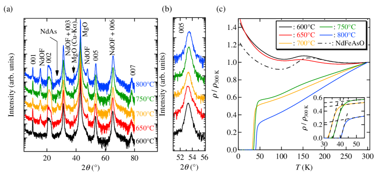
Figure 1(a) shows the XRD patterns of the NdFeAs(O,F) thin films for various deposition temperatures of the NdOF over-layer. All NdFeAs(O,F) films were grown -axis oriented. The diffraction peak of NdAs, which is a by-product of chemical reaction between NdOF and NdFeAsO, appeared above =700∘C. This is a natural consequence that higher deposition temperatures stimulate the chemical reaction. Another feature is a shift of the 00 reflections to higher angles with increasing , indicative of shortening the -axis length [fig. 1(b)]. It was reported that the -axis lattice parameter of LaFeAsO1-xFx [23] and CeFeAsO1-xFx [24] monotonously decreased with increasing F content. Hence, the observed change indicates that F diffuses into NdFeAsO and the amount of F in NdFeAs(O,F) increased with increasing the deposition temperature of the NdOF over-layer.
The temperature dependence of the normalised resistivity () varies with [fig. 1(c)]. Below =650∘C the normalised resistivity curves of the films were almost similar to those of the parent NdFeAsO. The upturn of at around 150 K corresponds to the structural transition from a high temperature tetragonal phase to a low temperature orthorhombic one. An onset of 38 K was recorded for the film with =700∘C. Further increase of the leads to an improvement of .
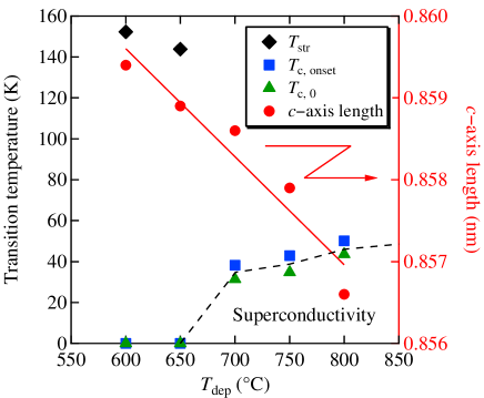
Figure 2 summarises the -axis lattice parameter and for the NdFeAs(O,F) films as a function of deposition temperature of NdOF. The -axis lattice parameter decreased almost linearly with increasing . Superconductivity can be induced by the deposition of NdOF at . From these results, the lowest with keeping superconductivity is determined to be 700∘C. In the following results, the NdOF over-layer was deposited at 700∘C.
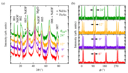
Structural characterisation of the NdFeAs(O,F) films grown on [001]-tilt symmetric MgO bicrystal substrates is summarised in fig. 3. The /2-scans showed that the NdFeAs(O,F) films were -axis oriented. The azimuthal -scan of the off-axis 102 reflection of NdFeAs(O,F) showed clearly eight peaks from two adjacent NdFeAs(O,F) grains separated by [fig. 3(b)]. Hence, the NdFeAs(O,F) films were grown epitaxially on [001]-tilt symmetric MgO bicrystal substrates.
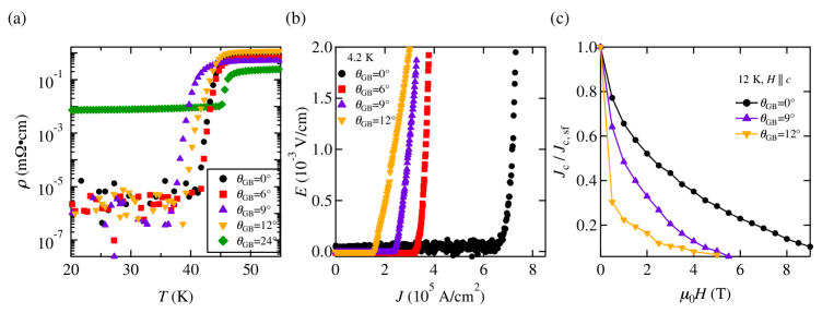
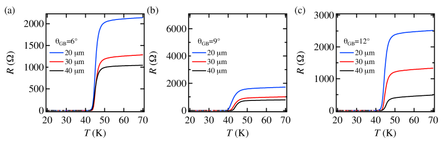
In fig. 4(a) the resistivity curves for the inter-grain bridges (bridge width =30 µ) with various misorientation angles are shown. For comparison the data of the intra-grain bridge (=0∘) fabricated from the NdFeAs(O,F) film with =6∘ are also plotted. As can be seen, the superconducting transition temperature did not systematically change with the grain boundary angle, which differs from our previous study (i.e. decreased with increasing ) [19]. The inter-grain bridges with =6∘ and 12∘ had an onset () of 45 K, which is almost the same as for the intra-grain bridges. For a wide transition width of 5 K was observed. As shown in Supplementary fig. S1, almost no difference in as well as the superconducting transition width were found with changing the bridge width.
A finite resistivity was observed for the inter-grain bridge with =24∘ below , whereas the other bridges showed a resistivity well below the instrumental limitation. Hence, the grain boundary region for =24∘ was destroyed by F even at =700, and accordingly, across the GB is zero.
Figure 4(b) compares the curves for the inter-grain bridges with various measured at 4.2 K without a magnetic field. The curve for the intra-grain bridge (=0∘) is also included, which exhibited a power-law behaviour described by , representing flux creep effects. The same behaviour was also seen for the inter-grain bridges with =6∘ and 9∘, which indicates that the two adjacent grains were strongly coupled. On the other hand, the inter-grain curve for =12∘ showed a non-Ohmic linear differential (NOLD) behaviour (i.e. is linearly changing with ) originating from viscous flux flow along the grain boundaries [25], indicative of limitation by grain boundaries [26]. The resistance area product for =12∘ was estimated to be 8.510-10 cm2, which is of the same order of magnitude for Co-doped Ba-122 with =45∘ (510-10 cm2)[11], P-doped Ba-122 with =24∘ (1.310-10 cm2)[15], and Fe(Se,Te) with =24∘ (710-10 cm2)[12]. Hence, the grain boundary of NdFeAs(O,F) is of metallic nature, which is similar to other FBS.
The field dependence of normalised to the self-field () plotted in fig. 4(c) also shows a typical behaviour of GB transport observed for FBS. For the bridge with =12∘, inter-grain was decreased by 70% even at a small applied magnetic field of 0.5 T, whereas the corresponding reduction for =0∘ (i.e. intra-grain) and =9∘ were 23% and 36%, respectively. Such a sharp drop of inter-grain for large by small magnetic fields is due to the weak coupling nature between adjacent grains.
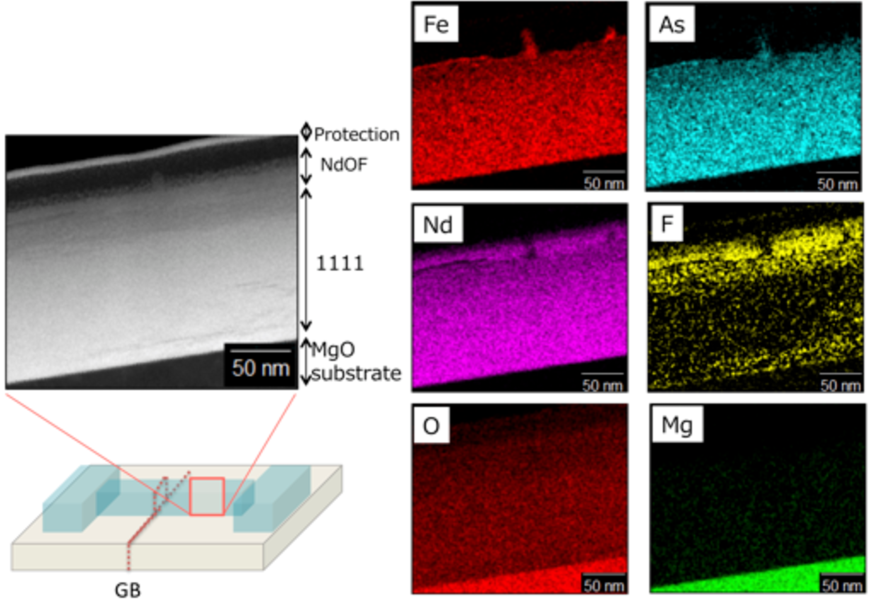
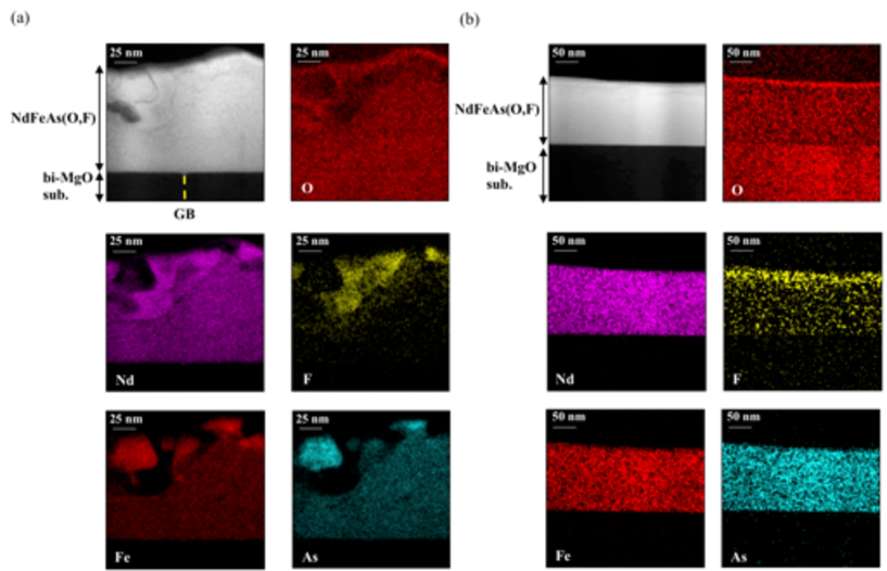
To further characterise the coupling between the grains with =6∘, microstructural observation by TEM was conducted [fig. 5(a)]. For comparison, the microstructures away from the GB region are also shown in fig. 5(b). The elemental mappings revealed a uniform distribution of all elements except for O and F [fig. 5(b)]. The observed high concentration of O and F at the surface region may be caused by heating due to Ar-ion milling to remove the NdOF over-layer. Uniform distribution of Nd, Fe, As, O and F within NdFeAs(O,F) was also observed in a different bridge (see Supplementary fig. S2). In stark contrast, the elemental distribution of the top region of NdFeAs(O,F) around the GB was strongly inhomogeneous due to the damage to NdFeAs(O,F) by F even though the deposition temperature of the NdOF over-layer was lowered [fig. 5(a)]. This is very similar to what was observed in our previous investigation[19]. However, the bottom region (about half of the thickness from the substrate) was quite uniform and free from damage by F. Hence, the grains are still coupled strongly in this region.
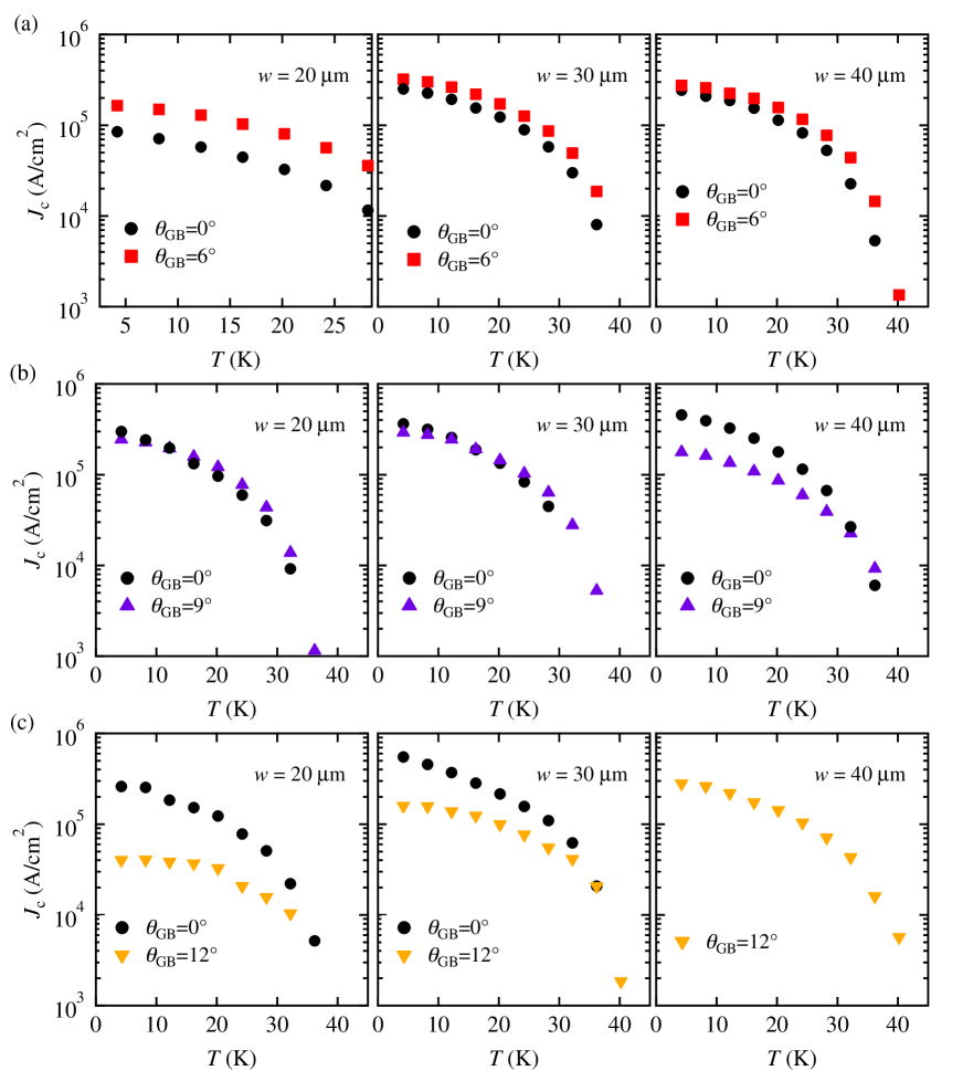
The temperature dependence of self-field for various misorientation angles are summarised in figs. 6(a)–(c). The intra-grain () of each film is also shown for comparison. Here, the measurements were conducted using 30 µ-wide bridges. The results obtained from various bridges are summarised in Supplementary fig. S3. The self-field of the intra-grain at low temperatures is in the order of A/cm2 for all three samples, which is one order of magnitude lower than our NdFeAs(O,F) films grown by employing =800 [27]. By comparing the at the same reduced temperatures (), of an ordinal NdFeAs(O,F) film prepared with =700 is smaller than that of a film with =800 [fig. 6(d)]. This is due to low carrier concentration. Hall effect measurements on our NdFeAs(O,F) films grown on single crystalline MgO revealed that the carrier concentration decreased from 1.981021 /cm3 for =800 to 1.341021 /cm3 for =750 at 50 K [28], although a precise evaluation of the carrier concentration is not easy due to the multi-band nature of the current superconductor. The carrier concentration of NdFeAs(O,F) for =700 is expected to be even smaller than that for =750, which probably explains the smaller .
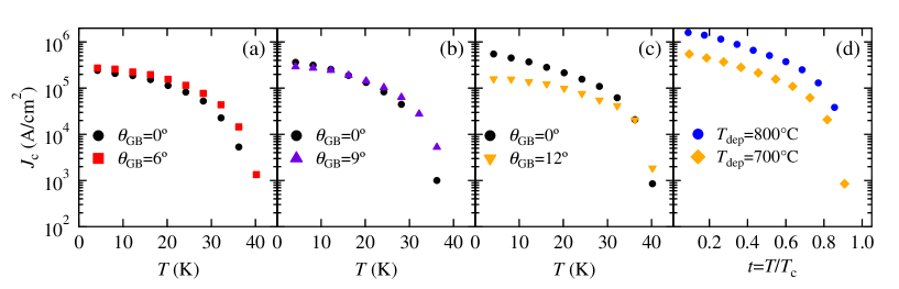
The distinct feature of the above results is that the respective inter-grain critical current densities () for =6∘ and are almost comparable to their intra-grain () at all temperatures [figs. 6(a), (b)], indicative of the absence of weak-links for both bicrystal films. For =12∘ below 32 K was certainly lower than . In Cu-Ag alloys it has been observed that the GBs are completely wetted by Ag when the misorientation angle is large [29]. It might be possible that F-rich phase had covered GBs and caused the transition from strong-link to weak-link behaviour. Nevertheless, at 4.2 K decreased by only 28% compared to in stark contrast to our previous study [19]. Note that the effective cross-sectional area in the vicinity of the GB with =6∘ was smaller than the intra-grain bridge as a consequence of the damage caused by F diffusion [see fig. 5(a)]. This is probably the reason why the plotted values are higher than in fig. 6(a), since was calculated by assuming that both the inter- and intra-grain bridges have the identical thickness.
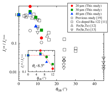
Figure 7 shows the dependence of the ratio of inter- to intra-grain () for the NdFeAs(O,F) bicrystal films at 4.2 K. For comparison the data of Co-doped Ba-122 at 4 K [11], Fe(Se,Te) at 4.2 K [12, 13], and our previous work on NdFeAs(O,F) at 4.2 K [19] are also plotted. The present work on NdFeAs(O,F) bicrystal films showed that was unity up to 8.5∘ (i.e. ), followed by a decrease with . On the other hand, was less than 6∘ in our previous investigation. These results indicate that the grain boundary properties were improved by lowering of NdOF. It is interesting that all FBS have a similar critical angle of around 9∘, suggesting that the symmetry of the superconducting order parameter for NdFeAs(O,F) may be the same as Co-doped Ba-122 and Fe(Se,Te).
Although =8.5∘ was determined for NdFeAs(O,F), it is still ambiguous how the inter-grain decreases with beyond 12∘. Additionally, it is not ruled out completely that the damage to the GB region by F had influenced the obtained results. To answer these issues and explore further the intrinsic GB characteristics, studying F-free oxypnictides, e.g. (Fe1-xCox)AsO [30, 31], would be interesting. Albeit the highest is around 25 K for Nd(Fe1-xCox)AsO [31], there would be no damage to the GB region by F. The misorientation angle dependence of for Nd(Fe1-xCox)AsO bicrystal films would be the direction of our future studies.
4 Summary
NdFeAs(O,F) epitaxial thin films were fabricated by MBE using a two-step process, where the deposition temperature () of NdOF was varied in the temperature range C. The -axis lattice parameter and of NdFeAs(O,F) changed systematically with of NdOF, and the F content in NdFeAs(O,F) increased with increasing . The lowest of NdOF without compromising was determined as 700∘C. By using =700 epitaxial NdFeAs(O,F) thin films were grown on [001]-tilt symmetric MgO bicrystal substrates with =6∘, 9∘, 12∘ and 24∘. Even for this reduced , however, the inter-grain bridge with =24∘ showed a finite resistance and hence was zero due to the erosion of NdFeAs(O,F) by F. Additionally, of the inter-grain bridges with and the intra-grain bridge were around 105 A/cm2 at low temperatures, which is almost one order of magnitude lower than NdFeAs(O,F) with =800 due probably to low carrier concentration. Nevertheless, the GB properties of the inter-grain bridges with lower were improved, resulting in a critical angle of =8.5∘. This critical angle is identical to Co-doped Ba-122 and Fe(Se,Te).
References
References
- [1] Putti M, Pallecchi I, Bellingeri E, Cimberle M R, Tropeano M, Ferdeghini C, Palenzona A, Tarantini C, Yamamoto A, Jiang J, Jaroszynski J, Kametani F, Abraimov D, Polyanskii A, Weiss J D, Hellstrom E E, Gurevich A, Larbalestier D C, Jin R, Sales B C, Sefat A S, McGuire M A, Mandrus D, Cheng P, Jia Y, Wen H H, Lee S and Eom C B, 2010 Supercond. Sci. Technol. 23 034003
- [2] Klein T, Braithwaite D, Demuer A, Knafo W, Lapertot G, Marcenat C, Rodière P, Sheikin I, Strobel P, Sulpice A and Toulemonde P, 2010 Phys. Rev. B 82 184506
- [3] Chaparro C, Fang L, Rydh A, Crabtree G W, Stantev V, Kwok W K and Welp U, 2012 Phys. Rev. B 85 184525
- [4] Kacmarcik J, Marcenat C, Klein T, Pribulova Z, van der Beek C J, Konczykowski M, Budko S L, Tillman M, Ni N and Canfield P C, 2009 Phys. Rev. B 80 014515
- [5] Adamski A, Krellner C and Abdel-Hafiez M, 2017 Phys. Rev. B 96 100503
- [6] Welp U, Chaparro C, Koshelev A E, Kwok W K, Rydh A, Zhigadlo N D, Karpinski J and Weyeneth S, 2011 Phys. Rev. B 83 100513
- [7] Mazin I I, Singh D J, Johannes M D and Du M H, 2008 Phys. Rev. Lett. 101 057003
- [8] Kuroki K, Onari S, Arita R, Usui H, Tanaka Y, Kontani H and Aoki H 2009 Phys. Rev. Lett. 101 087004
- [9] Hanaguri T, Niitaka S, Kuroki K and Takagi H 2010 Science 328 474
- [10] Tsuei C C and Kirtley J R 2000 Rev. Mod. Phys. 72 969
- [11] Katase T, Ishimaru Y, Tsukamoto A, Hiramatsu H, Kamiya T, Tanabe K and Hosono H 2011 Nat. Commun. 2 409
- [12] Si W, Zhang C, Shi X, Ozaki T, Jaroszynsski J and Li Q 2015 Appl. Phys. Lett. 106 032602
- [13] Sarnelli E, Nappi C, Camerlingo C, Enrico E, Bellingeri E, Kawale S, Braccini V, Leveratto A and Ferdeghini C 2017 IEEE. Trans. Appl. Supercond. 27 7400104
- [14] Hilgenkamp H and Mannhart J 2002 Rev. Mod. Phys. 74 485
- [15] Sakagami A, Kawaguchi T, Tabuchi M, Ujihara T, Takeda Y and Ikuta H 2013 Physica C 494 181
- [16] Zhang Q, Zhang X, Yao C, Huang H, Wang D, Dong C, Ma Y, Ogino H and Awaji S 2017 Supercond. Sci. Technol.30 065004
- [17] Iida K, Kurth F, Chihara M, Sumiya N, Grinenko V, Ichinose A, Tsukada I, Hänisch J, Matias V, Hatano T, Holzapfel B and Ikuta H 2014 Appl. Phys. Lett. 105 172602
- [18] Iida K, Hänisch J and Tarantini C 2018 Appl. Phys. Rev. 5 031304
- [19] Omura T, Matsumoto T, Hatano T, Iida K and Ikuta H 2018 J. Phys.: Conf. Ser. 1054 012024
- [20] Kawaguchi T, Uemura H, Ohno T, Tabuchi M, Ujihara T, Takenaka K, Takeda Y and Ikuta H 2010 Appl. Phys. Lett. 97 042509
- [21] Chihara M, Sumiya N, Arai K, Ichinose A, Tsukada I, Hatano T, Iida K and Ikuta H 2015 Physica C 518 69
- [22] Kawaguchi T, Uemura H, Ohno T, Tabuchi M, Ujihara T, Takeda Y and Ikuta H 2011 Appl. Phys. Express 4 083102
- [23] Huang Q, Zhao J, Lynn J W, Chen G F, Luo J L, Wang N L and Dai P 2008 Phys. Rev. B 78 054529
- [24] Zhao J, Huang Q, de la Cruz C, Li S, Lynn J W, Chen Y, Green M A, Chen G F, Li G, Li Z, Luo J L, Wang N L and Dai P 2008 Nat. Mater. 7 953
- [25] Díaz A, Mechin L, Berghuis P and Evetts J E 1998 Phys. Rev. B 58 R2960
- [26] Verebelyi D T, Christen D K, Feenstra R, Cantoni C, Goyal A, Lee D F, Paranthaman M, Arendt P N, DePaula R F, Groves J R and Prouteau C 2000 Appl. Phys. Lett. 76 1755
- [27] Chiara T, Iida K, Hänisch J, Kurth F, Jaroszynski J, Sumiya N, Chihara M, Hatano T, Ikuta H, Schmidt S, Seidel P, Holzapfel B and Larbalestier D C 2016 Sci. Rep. 6 36047
- [28] Matsumoto T, Kondo K, Hatano T, Iida K and Ikuta H in preparation
- [29] Straumal B B, Bokshtein B S, Straumal A B and Petelin A L 2008 JETP Letters 88 537
- [30] Wang C, Li Y K, Zhu Z W, Jiang S, Lin X, Luo Y K, Chi S, Li L J, Ren Z, He M, Chen H, Wang Y T, Tao Q, Cao G H and Xu Z A 2009 Phys. Rev. B 79 054521
- [31] Kim S K, Tillman M E, Kim H, Kracher A, Bud’ko S L, Prozorov R and Canfield P C, 2010 Supercond. Sci. Technol. 23 054008
Supplementary information