Fragility of Fermi arcs in Dirac semimetals
Abstract
We use tunable, vacuum ultraviolet laser-based angle-resolved photoemission spectroscopy and density functional theory calculations to study the electronic properties of Dirac semimetal candidate cubic PtBi2. In addition to bulk electronic states we also find surface states in PtBi2 which is expected as PtBi2 was theoretical predicated to be a candidate Dirac semimetal. The surface states are also well reproduced from DFT band calculations. Interestingly, the topological surface states form Fermi contours rather than double Fermi arcs that were observed in Na3Bi. The surface bands forming the Fermi contours merge with bulk bands in proximity of the Dirac points projections, as expected. Our data confirms existence of Dirac states in PtBi2 and reveals the fragility of the Fermi arcs in Dirac semimetals. Because the Fermi arcs are not topologically protected in general, they can be deformed into Fermi contours, as proposed by [Kargarian et al., PNAS 113, 8648 (2016)]. Our results demonstrate validity of this theory in PtBi2.


Topological materials hosting Dirac fermions, Weyl fermions, and Majorana fermions are recognized as having the potential to revolutionize the field of high-performance electronics and fault-tolerant quantum computing Nayak et al. (2008). The focus on topological materials started with two-dimensional (2D) Dirac states discovered either in 2D materials such as graphene Geim and Novoselov (2007) or on the surface of three-dimensional (3D) topological insulators Zhang et al. (2009); Xia et al. (2009); Chen et al. (2009). Generalizing the 2D Dirac states to the 3D case leads us to the era of 3D Dirac and Weyl semimetals. Na3Bi and Cd3As2 are the two archetypical 3D Dirac semimetals, where the bulk Dirac points are protected by crystal symmetry Liu et al. (2014a); Neupane et al. (2014); Liu et al. (2014b). Breaking either the time-reversal Wang et al. (2016) or inversion symmetry Xu et al. (2015a) of a 3D Dirac semimetal can result in a Weyl semimetal with pairs of Weyl nodes that have opposite chirality. The Weyl nodes are monopoles in the Berry curvature with non-zero Chern number that naturally lead to exotic surface states such as Fermi arcs. The discovery of Fermi arcs in both type-I Xu et al. (2015a) and type-II Huang et al. (2016); Tamai et al. (2016); Deng et al. (2016) Weyl semimetals confirmed the existence of these exotic states. Although Fermi arc surface states have been predicted Wang et al. (2012, 2013) and observed in 3D Dirac semimetals Xu et al. (2015b); Yi et al. (2014), the topological nature and stability of these surface states are still under debate Kargarian et al. (2016); Armitage et al. (2018).
Here we demonstrate that the measured surface and bulk band structure of cubic PtBi2 agrees well with calculations and confirms that it is a Dirac semimetal. We further demonstrate that the surface state in this system forms closed Fermi contours rather than double Fermi arcs as reported in Na3Bi Xu et al. (2015b). Since the Fermi arcs in Dirac semimetals are not topologically protected, they can be deformed into closed Fermi contours by a strong surface potential. This was first proposed by Kargarian et al. Kargarian et al. (2016) and our data confirms that this indeed occurs in cubic PtBi2. Our results point to fragility of Fermi arcs in Dirac semimetals due to lack of topological protection.
PtBi2 crystallizes in at least four phases, one of which is a pyrite type with simple cubic crystal structure (space group 205). The pyrite type PtBi2 was predicted to host 3D Dirac points along the - line, which are protected by the threefold rotational symmetry Gibson et al. (2015). Similar to some of the topological materials, such as Dirac node arc metal PtSn4 Mun et al. (2012); Wu et al. (2016), Dirac semimetal Cd3As2 Liang et al. (2015), and type-II Weyl semimetal WTe2 Ali et al. (2014), cubic PtBi2 also exhibit extremely large magnetoresistance up to (11.2)% at K in a magnetic field of 33 T Gao et al. (2017). Interestingly, another phase, hexagonal PtBi2 also exhibits giant magnetoresistance Yang et al. (2016). Topological surface states have been predicted Xu et al. (2016) and observed Yao et al. (2016); Thirupathaiah et al. (2018) in hexagonal PtBi2. However, no evidence of the 3D Dirac semimetallic state has been reported in cubic PtBi2 as of yet.
Single crystals of PtBi2 were grown out of Bi rich binary melts. Elemental Pt and Bi were put into a Canfield Crucible Set Canfield et al. (2016) with initial stoichiometry, Pt0.05Bi0.95, and sealed into an amorphous silica tube. The ampules were heated up to 430 within 5 hours, held for 5 hours, cooled to 300 \celsius over 75 hours, and finally decanted using a centrifuge Canfield and Fisk (1992). Single crystals obtained from the growth were ground to obtain a room temperature powder x-ray diffraction (XRD) pattern with a Rigaku MiniFlex II diffractometer (Cu radiation with monochromator).
Band structures with spin-orbit coupling (SOC) in density functional theory (DFT) Hohenberg and Kohn (1964); Kohn and Sham (1965) have been calculated using a PBE Perdew et al. (1996) exchange-correlation functional, a plane-wave basis set and projector augmented wave method Blöchl (1994) as implemented in VASP Kresse and Furthmüller (1996, 1996). For the bulk band structure of cubic PtBi2, we used the primitive cubic cell of 12 atoms with a Monkhorst-Pack Monkhorst and Pack (1976) () -point mesh including the point and a kinetic energy cutoff of 230 eV. The convergence with respect to -point mesh was carefully checked, with total energy converged below 1 meV/atom. The experimental lattice parameters have been used with atoms fixed in their bulk positions. A tight-binding model based on maximally localized Wannier functions Marzari and Vanderbilt (1997); Souza et al. (2001); Marzari et al. (2012) was constructed to reproduce closely the bulk band structure including SOC in the range of 1 eV with Pt and Bi orbitals. Subsequently, the Fermi surface and spectral functions of a semi-infinite PtBi2 (001) surface, with Bi-termination, were calculated by using the surface Green’s function methods Lee and Joannopoulos (1981a, b); Sancho et al. (1984, 1985) as implemented in WannierTools Wu et al. (2017).
Samples used for ARPES measurements were cleaved in situ at 40 K under ultrahigh vacuum (UHV). The data were acquired using a tunable VUV laser ARPES system, that consists of a Scienta R8000 electron analyzer, a picosecond Ti:Sapphire oscillator and fourth harmonic generator Jiang et al. (2014). Data were collected with a photon energy of 6.7 eV. Momentum and energy resolutions were set at 0.005 Å-1 and 2 meV. The size of the photon beam on the sample was 30 m.
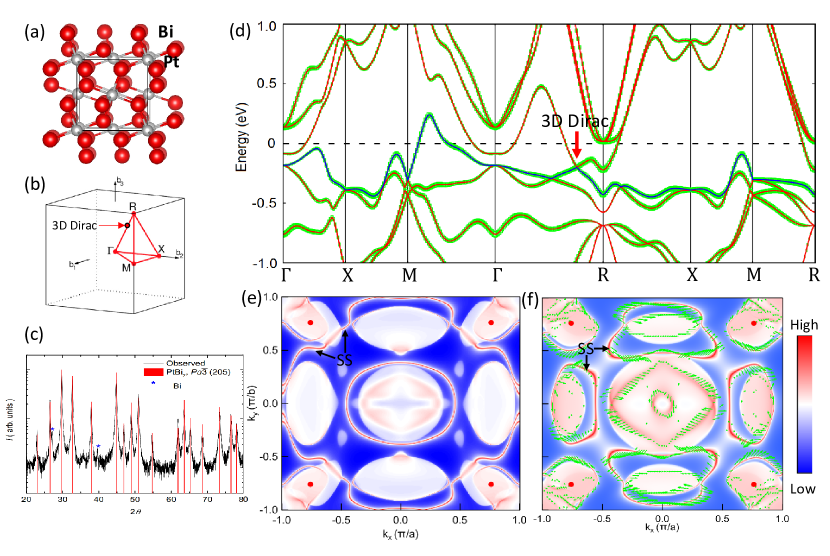
Figure 1 shows the crystal structure and calculated electronic structure of PtBi2. Fig. 1(a) shows the crystal structure of cubic PtBi2, where the red and white spheres correspond to Bi and Pt atoms, respectively. The acquired XRD patterns are well matched with calculated peaks for pyrite structure type of PtBi2 with (205) as shown in Fig. 1(c). The small intensity, extra peaks, marked with blue stars, are associated with residual Bi solvent left on the surface of the crystals. Fig. 1(d) presents the bulk electronic structure with the red arrow points to the 3D Dirac point along the - line, consistent with the results in Ref. Gibson et al., 2015. The coordinates of the bulk Dirac points are (0.76, 0.76, 0.76) and at meV (Fig. 1d). The green shading represents the magnitude of the projection on orbitals. The constant energy contours calculated with surface Green’s function using a semi-infinite PtBi2 (001) surface with Bi-termination are shown in Figs. 1(e) and (f). The bulk bands are projected onto a plane and therefore appear as white patches with various degree of red. The surface states are the sharp lines mostly going through the bulk gap regions and sometimes connecting with the bulk states. The green arrows in Fig. 1(f) shows the spin texture of the surface states with a helical structure similar to Na3Bi Wang et al. (2012). The red dots are the projections of the 3D Dirac points onto the surface Brillouin zone. Interestingly, at Fermi level (), there are distinct Fermi arc surface states connecting the projections of the 3D Dirac point; whereas at 100 meV above , the “Fermi arc” surface states break from the bulk projections and form closed loops in between Dirac nodes projections. This calculation result is consistent with the theoretical model in Ref. Kargarian et al., 2016, demonstrating the fragility of the “Fermi arc” surface states in 3D Dirac semimetals.
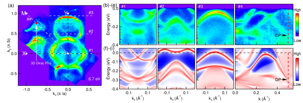
Next, we present detailed ARPES measurements to compare with the results of band structure calculations. Fig. 2(a) shows the ARPES intensity map of PtBi2 integrated within 10 meV about the chemical potential. The Fermi surface is generated by overlaying two data sets measured along 0∘ and 45∘ with respect to the crystal axis. The Fermi surface consists of an electron pocket at the center and several hole pockets along the high symmetry lines. Interestingly, the FS in ARPES resembles the FS calculation at 100 meV above , where the topological surface states are completely disconnected from the projection of the 3D Dirac point (the red solid dot). This chemical potential shift can be better visualized by comparing the band dispersions from ARPES measurements and band structure calculations. The band dispersions along cuts #1 to #4 from ARPES and DFT calculations are shown in Figs. 2(b)–(e) and (f)–(i), respectively. We can clearly see that the experimental and theoretical results match very well, except that the chemical potential in the calculations needs to be shifted upwards by roughly 100 meV to achieve good agreement. This works luckily to our advantage, saving us the trouble to purposely dope PtBi2 with electrons in order to verify the fragility of the “Fermi arc” surface states as shown in Fig. 1. Furthermore, by comparing with the calculation results, we can conclude that the high intensity Fermi surface sheets along - and - directions in the ARPES data are actually surface states.
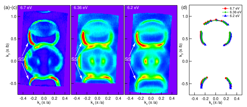
In order to verify that the high intensity Fermi surface sheets indeed have a surface origin, we performed photon energy dependent measurements as shown in Fig. 3. Figs. 3(a), (b), and (c) show the Fermi surface plots of PtBi2 measured using 6.7, 6.36, and 6.05 eV photons. We can clearly see that the surface states have almost the same intensity profile, whereas the states close to the center of the Brillouin zone vary significantly with different photon energies. To better quantify our observations, we plotted the fitted results of the high intensity locations in Fig. 3(d). It is clear that the SS measured from three different photon energies almost perfectly match each other. This photon energy independent characteristic, in tandem with the good match between ARPES and DFT calculations, provide solid arguments for the surface origin of these states.
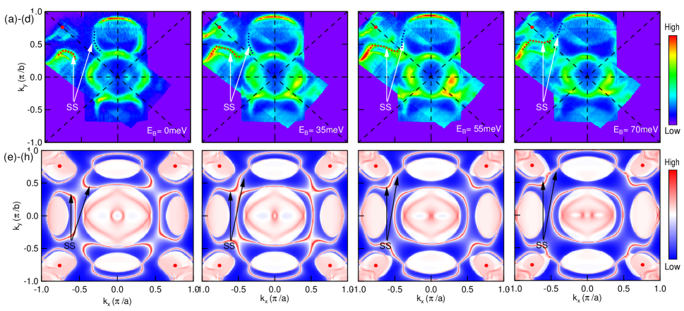
To demonstrate the fragility of the “Fermi arc” surface states in this Dirac semimetal, we plot the constant energy contours at different binding energies in Fig. 4. The red dots in Fig. 4 are the projections of the 3D Dirac points along - line. In Fig. 4(a), we can clearly see the surface states forming closed loops are well separated from the bulk states containing the projection of the 3D Dirac point (red dot). This can be better visualized in Fig. 4(e), the corresponding surface calculations. Moving down in binding energy, we can see the surface state along the - direction starts to detach from the electron pocket surrounding the point and moving closer to the other surface states along - direction. As we move further down to the binding energy of 55 meV, both surface states along - and - directions start to move closer to the bulk states containing the 3D Dirac point projection. Finally, at =70 meV, both surface states merge with the bulk states, matching well the calculation results shown in Fig. 4(h). The blue and red dashed lines are guides to the eye marking the path of the surface states. This demonstrates that the topological surface states evolve from closed loops completely dissociated from the projection of 3D Dirac point to actual arc states connecting the bulk states containing the projections. This is a definite experimental proof of the calculation results in Fig. 1 and the theoretical model in Ref. Kargarian et al., 2016. Thus, we show the Fermi arc surface states in this Dirac semimetal are not topological protected and they change from arcs to closed-loops by varying the binding energy. Because there are an even number of (four, to be specific) pairs of Dirac points not located at time reversal invariant momentum locations in PtBi2, it belongs to the “weak” Dirac semimetal category, i.e., the surface states observed in PtBi2 could be gapped out by translation symmetry-breaking perturbations Kargarian et al. (2016).
In conclusion, we use ultrahigh resolution ARPES and DFT calculations to demonstrate that the “Fermi arc” surface states in 3D Dirac semimetal cubic PtBi2 is not topologically protected, in stark contrast to the Fermi arc surface states in Weyl semimetals. At one binding energy ( meV), the surface states display an arc form connecting the bulk states containing the projections of the 3D Dirac points. At another binding energy (), they become completely disconnected from the projections of the Dirac point and form closed loops in-between the projections at the Fermi level. This demonstrates the fragility of the “Fermi arc” surface states in 3D Dirac semimetal cubic PtBi2, consistent with the theoretical model proposed in Ref. Kargarian et al., 2016. Furthermore, we observe a Fermi arc-like surface state along - direction which is not obvious in DFT calculations. More thorough theoretical understanding is required to better explore the topological nature of this state.
We would like to thank Mohit Randeria, Yuan-Ming Lu and Peter Orth for very useful comments. Research was supported by the U.S. Department of Energy, Office of Basic Energy Sciences, Division of Materials Science and Engineering. Ames Laboratory is operated for the U.S. Department of Energy by Iowa State University under Contract No. DE-AC02-07CH11358. Y. W. and L. L. W. were supported by Ames Laboratory’s Laboratory-Directed Research and Development (LDRD) funding. N.H.J. was supported by the Gordon and Betty Moore Foundation EPiQS Initiative (Grant No. GBMF4411). B. S. was supported by CEM, a NSF MRSEC, under Grant No. DMR-1420451.
Raw data for this manuscript will be available from the authors upon reasonable request.
References
- Nayak et al. (2008) C. Nayak, S. H. Simon, A. Stern, M. Freedman, and S. Das Sarma, Rev. Mod. Phys. 80, 1083 (2008).
- Geim and Novoselov (2007) A. K. Geim and K. S. Novoselov, Nat Mater 6, 183 (2007).
- Zhang et al. (2009) H. Zhang, C.-X. Liu, X.-L. Qi, X. Dai, Z. Fang, and S.-C. Zhang, Nat. Phys. 5, 438 (2009).
- Xia et al. (2009) Y. Xia, D. Qian, D. Hsieh, L. Wray, A. Pal, H. Lin, A. Bansil, D. Grauer, Y. S. Hor, R. J. Cava, and M. Z. Hasan, Nat. Phys. 5, 398 (2009).
- Chen et al. (2009) Y. L. Chen, J. G. Analytis, J.-H. Chu, Z. K. Liu, S.-K. Mo, X. L. Qi, H. J. Zhang, D. H. Lu, X. Dai, Z. Fang, S. C. Zhang, I. R. Fisher, Z. Hussain, and Z.-X. Shen, Science 325, 178 (2009).
- Liu et al. (2014a) Z. K. Liu, B. Zhou, Y. Zhang, Z. J. Wang, H. M. Weng, D. Prabhakaran, S.-K. Mo, Z. X. Shen, Z. Fang, X. Dai, Z. Hussain, and Y. L. Chen, Science 343, 864 (2014a).
- Neupane et al. (2014) M. Neupane, S. Xu, R. Sankar, N. Alidoust, G. Bian, C. Liu, I. Belopolski, T. Chang, H. Jeng, H. Lin, A. Bansil, F. Chou, and M. Z. Hasan, Nat Commun 5 (2014).
- Liu et al. (2014b) Z. K. Liu, J. Jiang, B. Zhou, Z. J. Wang, Y. Zhang, H. M. Weng, D. Prabhakaran, S.-K. Mo, H. Peng, P. Dudin, T. Kim, M. Hoesch, Z. Fang, X. Dai, Z. X. Shen, D. L. Feng, Z. Hussain, and Y. L. Chen, Nat Mater 13, 677 (2014b).
- Wang et al. (2016) Z. Wang, M. G. Vergniory, S. Kushwaha, M. Hirschberger, E. V. Chulkov, A. Ernst, N. P. Ong, R. J. Cava, and B. A. Bernevig, Phys. Rev. Lett. 117, 236401 (2016).
- Xu et al. (2015a) S.-Y. Xu, I. Belopolski, N. Alidoust, M. Neupane, G. Bian, C. Zhang, R. Sankar, G. Chang, Z. Yuan, C.-C. Lee, S.-M. Huang, H. Zheng, J. Ma, D. S. Sanchez, B. Wang, A. Bansil, F. Chou, P. P. Shibayev, H. Lin, S. Jia, and M. Z. Hasan, Science 349, 613 (2015a).
- Huang et al. (2016) L. Huang, T. M. McCormick, M. Ochi, Z. Zhao, M. Suzuki, R. Arita, Y. Wu, D. Mou, H. Cao, J. Yan, N. Trivedi, and A. Kaminski, Nat Mater 15, 1155 (2016).
- Tamai et al. (2016) A. Tamai, Q. S. Wu, I. Cucchi, F. Y. Bruno, S. Riccò, T. K. Kim, M. Hoesch, C. Barreteau, E. Giannini, C. Besnard, A. A. Soluyanov, and F. Baumberger, Phys. Rev. X 6, 031021 (2016).
- Deng et al. (2016) K. Deng, G. Wan, P. Deng, K. Zhang, S. Ding, E. Wang, M. Yan, H. Huang, H. Zhang, Z. Xu, J. Denlinger, A. Fedorov, H. Yang, W. Duan, H. Yao, Y. Wu, S. Fan, H. Zhang, X. Chen, and S. Zhou, Nat Phys 12, 1105 (2016).
- Wang et al. (2012) Z. Wang, Y. Sun, X.-Q. Chen, C. Franchini, G. Xu, H. Weng, X. Dai, and Z. Fang, Phys. Rev. B 85, 195320 (2012).
- Wang et al. (2013) Z. Wang, H. Weng, Q. Wu, X. Dai, and Z. Fang, Phys. Rev. B 88, 125427 (2013).
- Xu et al. (2015b) S.-Y. Xu, C. Liu, S. K. Kushwaha, R. Sankar, J. W. Krizan, I. Belopolski, M. Neupane, G. Bian, N. Alidoust, T.-R. Chang, H.-T. Jeng, C.-Y. Huang, W.-F. Tsai, H. Lin, P. P. Shibayev, F.-C. Chou, R. J. Cava, and M. Z. Hasan, Science 347, 294 (2015b).
- Yi et al. (2014) H. Yi, Z. Wang, C. Chen, Y. Shi, Y. Feng, A. Liang, Z. Xie, S. He, J. He, Y. Peng, X. Liu, Y. Liu, L. Zhao, G. Liu, X. Dong, J. Zhang, M. Nakatake, M. Arita, K. Shimada, H. Namatame, M. Taniguchi, Z. Xu, C. Chen, X. Dai, Z. Fang, and X. J. Zhou, Sci. Rep. 4 (2014).
- Kargarian et al. (2016) M. Kargarian, M. Randeria, and Y.-M. Lu, Proceedings of the National Academy of Sciences 113, 8648 (2016).
- Armitage et al. (2018) N. P. Armitage, E. J. Mele, and A. Vishwanath, Rev. Mod. Phys. 90, 015001 (2018).
- Gibson et al. (2015) Q. D. Gibson, L. M. Schoop, L. Muechler, L. S. Xie, M. Hirschberger, N. P. Ong, R. Car, and R. J. Cava, Phys. Rev. B 91, 205128 (2015).
- Mun et al. (2012) E. Mun, H. Ko, G. J. Miller, G. D. Samolyuk, S. L. Bud’ko, and P. C. Canfield, Phys. Rev. B 85, 035135 (2012).
- Wu et al. (2016) Y. Wu, L. Wang, E. Mun, D. D. Johnson, D. Mou, L. Huang, Y. Lee, S. L. Bud/’ko, P. C. Canfield, and A. Kaminski, Nat Phys 12, 667 (2016).
- Liang et al. (2015) T. Liang, Q. Gibson, M. N. Ali, M. Liu, R. J. Cava, and N. P. Ong, Nat Mater 14, 280 (2015).
- Ali et al. (2014) M. N. Ali, J. Xiong, S. Flynn, J. Tao, Q. D. Gibson, L. M. Schoop, T. Liang, N. Haldolaarachchige, M. Hirschberger, N. P. Ong, and R. J. Cava, Nature 514, 205 (2014).
- Gao et al. (2017) W. Gao, N. Hao, F.-W. Zheng, W. Ning, M. Wu, X. Zhu, G. Zheng, J. Zhang, J. Lu, H. Zhang, C. Xi, J. Yang, H. Du, P. Zhang, Y. Zhang, and M. Tian, Phys. Rev. Lett. 118, 256601 (2017).
- Yang et al. (2016) X. Yang, H. Bai, Z. Wang, Y. Li, Q. Chen, J. Chen, Y. Li, C. Feng, Y. Zheng, and Z. an Xu, Applied Physics Letters 108, 252401 (2016).
- Xu et al. (2016) C. Q. Xu, X. Z. Xing, X. Xu, B. Li, B. Chen, L. Q. Che, X. Lu, J. Dai, and Z. X. Shi, Phys. Rev. B 94, 165119 (2016).
- Yao et al. (2016) Q. Yao, Y. P. Du, X. J. Yang, Y. Zheng, D. F. Xu, X. H. Niu, X. P. Shen, H. F. Yang, P. Dudin, T. K. Kim, M. Hoesch, I. Vobornik, Z.-A. Xu, X. G. Wan, D. L. Feng, and D. W. Shen, Phys. Rev. B 94, 235140 (2016).
- Thirupathaiah et al. (2018) S. Thirupathaiah, Y. Kushnirenko, E. Haubold, A. V. Fedorov, E. D. L. Rienks, T. K. Kim, A. N. Yaresko, C. G. F. Blum, S. Aswartham, B. Büchner, and S. V. Borisenko, Phys. Rev. B 97, 035133 (2018).
- Canfield et al. (2016) P. C. Canfield, T. Kong, U. S. Kaluarachchi, and N. H. Jo, Philosophical Magazine 96, 84 (2016).
- Canfield and Fisk (1992) P. C. Canfield and Z. Fisk, Philosophical Magazine Part B 65, 1117 (1992).
- Hohenberg and Kohn (1964) P. Hohenberg and W. Kohn, Phys. Rev. 136, B864 (1964).
- Kohn and Sham (1965) W. Kohn and L. J. Sham, Phys. Rev. 140, A1133 (1965).
- Perdew et al. (1996) J. P. Perdew, K. Burke, and M. Ernzerhof, Phys. Rev. Lett. 77, 3865 (1996).
- Blöchl (1994) P. E. Blöchl, Phys. Rev. B 50, 17953 (1994).
- Kresse and Furthmüller (1996) G. Kresse and J. Furthmüller, Phys. Rev. B 54, 11169 (1996).
- Kresse and Furthmüller (1996) G. Kresse and J. Furthmüller, Computational Materials Science 6, 15 (1996).
- Monkhorst and Pack (1976) H. J. Monkhorst and J. D. Pack, Phys. Rev. B 13, 5188 (1976).
- Marzari and Vanderbilt (1997) N. Marzari and D. Vanderbilt, Phys. Rev. B 56, 12847 (1997).
- Souza et al. (2001) I. Souza, N. Marzari, and D. Vanderbilt, Phys. Rev. B 65, 035109 (2001).
- Marzari et al. (2012) N. Marzari, A. A. Mostofi, J. R. Yates, I. Souza, and D. Vanderbilt, Rev. Mod. Phys. 84, 1419 (2012).
- Lee and Joannopoulos (1981a) D. H. Lee and J. D. Joannopoulos, Phys. Rev. B 23, 4988 (1981a).
- Lee and Joannopoulos (1981b) D. H. Lee and J. D. Joannopoulos, Phys. Rev. B 23, 4997 (1981b).
- Sancho et al. (1984) M. P. L. Sancho, J. M. L. Sancho, and J. Rubio, Journal of Physics F: Metal Physics 14, 1205 (1984).
- Sancho et al. (1985) M. P. L. Sancho, J. M. L. Sancho, J. M. L. Sancho, and J. Rubio, Journal of Physics F: Metal Physics 15, 851 (1985).
- Wu et al. (2017) Q. Wu, S. Zhang, H.-F. Song, M. Troyer, and A. A. Soluyanov, arXiv preprint arXiv:1703.07789 (2017).
- Jiang et al. (2014) R. Jiang, D. Mou, Y. Wu, L. Huang, C. D. McMillen, J. Kolis, H. G. Giesber, J. J. Egan, and A. Kaminski, Review of Scientific Instruments 85, 033902 (2014).