Evidence of Majorana Zero Modes in Josephson Trijunctions
Abstract
In search of fault-tolerant topological quantum computation (TQC), zero-bias conductance peak as a necessary signature of Majorana zero modes (MZMs) has been observed in a number of solid-state systems. Here, we present the signature of MZMs from a phase-sensitive experiment on Josephson trijunctions constructed on the surface of three-dimensional topological insulators. We observed that the minigap at the center of the trijunction is protected to close over extended regions in phase space, supporting in principle the Majorana phase diagram proposed by Fu and Kane in 2008. Our study paves the way for further braiding MZMs and exploring TQC on a scalable two-dimensional platform.
It is believed that fault-tolerant TQC can be realized by encoding quantum information on topologically protected quantum states 1 ; 2 ; 3 . In 2001, Kitaev proposed the use of p-wave superconducting chains to host MZMs as topological qubits 4 . In 2008, Fu and Kane further proposed to induce p-wave-like superconductivity from s-wave superconductors via proximity effect in a hybrid structure 5 . Since then, many hybrid structures have been proposed 6 ; 7 ; 8 ; 9 ; 10 , and signatures of MZMs have been observed in structures containing semiconducting nanowires 11 ; 12 ; 13 ; 14 ; 15 , topological insulators 16 ; 17 ; 18 ; 19 ; 20 , iron chains 22 , etc. However, the original proposal of Fu and Kane – to construct Josephson trijunctions on topological insulators 5 , which could potentially serve as the basic components for universal TQC 23 ; 24 – remains unexplored.
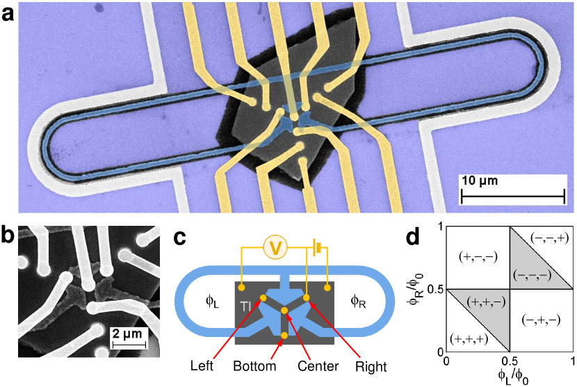
According to Fu and Kane 5 , for Josephson trijunctions constructed on the surface of a three-dimensional topological insulator (3D TI), there will be a boundary at the center isolating the single junctions with positive minigap to those with negative minigap, when gap-inversion occurs in odd numbers of single junctions. Such a boundary, at which the minigap closes completely and a localized MZM appears, is protected to occur over extended parametric regions with nontrivial topological numbers, as illustrated in Fig. 1d. The verification of complete minigap-closing over extended regions in phase space, in analogy to various quantum Hall edge states surviving over extended parametric regions, would provide strong evidence for the existence of MZMs in TI-based Josephson devices.
In this experiment, we fabricated Josephson trijunctions on the surface of Bi2Te3 flakes and used magnetic flux to control the phase differences in the junctions. Figure 1a and 1b are the scanning electron microscopic (SEM) image of such a device. The three superconducting Pb pads, separated by 560 nm, couple with each other through Bi2Te3 to form Josephson junctions. The phase differences across the junctions can be adjusted either simultaneously by applying a global magnetic field, or individually by applying local currents to the two half-turn coils. The Andreev bound states (ABSs) of the trijunction can be detected by measuring the contact resistance of the Au electrodes, which contact the Bi2Te3 surface at the center and the ends through windows on the blackish-looking insulating mask made of over-exposed polymethyl methacrylate (PMMA). For further information on device fabrication and measurement configuration please see the supplementary materials 25 .
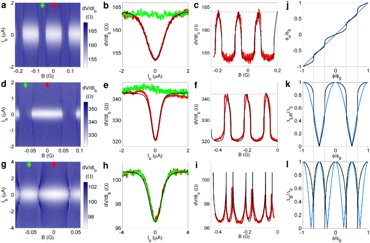
Let us first look at the data measured at the ends of the 1st trijunction. Figure 2a shows the differential contact resistance of the Au electrodes at the left end as functions of global magnetic field and bias current . Figure 2b shows the vertical line cuts of the data in Fig. 2a, namely the curves, at global magnetic fields indicated by the arrows with corresponding color in Fig. 2a. Figure 2c shows the horizontal line cut of the data, namely the curve, at =0. Figure 2d, 2e, 2f, and Fig. 2g, 2h, 2i show similar data obtained at the right and the bottom ends of the trijunction, respectively. The measurements were performed at 0.5 K to avoid hysteresis (will be explained later).
We can see that the at the left and the right ends shows similar behaviors. When the curves in Fig. 2c and 2f enter into a low-resistance state, the curves demonstrate a pronounced valley centering at zero bias (the red curves in Fig. 2b and 2e). When the curves touch the normal-state value represented by the dashed lines in Fig. 2c and 2f, the curves become constant (the green curves in Fig. 2b, 2e). At the bottom end of the trijunction, differently, the low-resistance state at zero bias remains at most magnetic fields (Fig. 2g, 2i) — the approaches to the normal-state value only temporally during the field sweeping.
The following is our explanation for the observed phenomena. It is known from previous studies 20 that the minigap in the junction can be modulated from open to closed by varying the phase difference of the junction via 5 ; 26 ; 27 : (where is the induced gap). This minigap predominantly determines the contact resistance of the Au-Bi2Te3 interface. When the interface is in the transparent regime, which is the case for the 1st and the 2nd (shown in Fig. 4) devices, the will be reduced within the minigap, due to Andreev reflections between Au and the induced superconducting Bi2Te3. When the interface is in the tunneling regime, e.g., for the 3rd and the 4th devices (shown in Fig. 4 and in the supplementary materials), the will be enhanced within the minigap. In both regimes, the can be described by the Blonder-Tinkham-Klapwijk (BTK) theory 28 .
Through fitting the zero-magnetic-field curves in Fig. 2b, 2e and 2h using the BTK theory (the black lines), the barrier parameters of the Au contacts as well as the minigap beneath the contacts can be obtained — for the left end eV, the number of channel =134, the barrier strength =0.843; for the right end eV, =63, =0.825; and for the bottom end eV, =200, =0.753. The details can be found in the supplementary materials 25 .
An applied magnetic flux in the superconducting loop modifies the phase difference across the junctions, hence modifies the minigap in the junctions. When the field-induced screening supercurrents in the loop is negligibly small, namely the screening parameter 29 : approaches to zero (where is the inductance of a single loop, the bulk critical supercurrent 20 of the single junction, and the flux quantum), we simply have , so , as represented by the blue lines in Fig. 2k, 2l. Otherwise, when the screening supercurrent cannot be neglected, , where the effective magnetic flux obeys the relation . In particular, when exceeds 0.5 (instead of 1, since the total screening supercurrent in one loop is 2 in our devices), becomes multi-valued, so that hysteresis occurs during backward and forward field sweepings. We did observe hysteretic responses of at the base temperature. The results are shown in the supplementary materials 25 .
The data presented in Fig. 2 were collected at an elevated temperature of 0.5 K, at which the critical supercurrent was reduced such that the hysteretic behavior marginally disappeared, corresponding to the case of 0.5. In this case, the effective magnetic flux follows the warping line in Fig. 2j. As a result, the field dependence of the minigap in the left and right junctions (bottom junction) is modified to the black line in Fig. 2k (Fig. 2l).
With these field-dependent functional forms of minigap, together with the fitting parameters including obtained from the vs. curves, the global magnetic field dependences of can be simulated by using the BTK theory. The results of simulation are shown as the black lines in Fig. 2c, 2f and 2i. Good agreements with the experimental data are obtained.
One noticeable feature in Fig. 2c, 2f and 2i is that the approaches to and leaves away the normal-state value (the dashed lines) sharply, showing a linear closing of the minigap, intuitively hinting that the underlying mechanism of gap-closing and re-opening is a sign-change process originated from a 4 periodicity, by which the complete closing of minigap (i.e., crossing of electron-like and hole-like ABSs) is guaranteed. We note that for trivial Josephson single junctions or trijunctions, the minigap will never oscillate to zero, due to unavoidable anti-crossing between electron-like and hole-like ABSs, even in highly transparent atomic point contacts 30 or S-N-S junctions with N being a single graphene layer 31 . The observation of full transparency in our Pb-Bi2Te3-Pb junctions, in which the two Pb electrodes are separated as far away as 560 nm, has to arise from a topologically protected mechanism based on MBSs, as has been studied previously 20 .
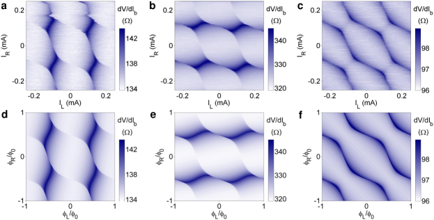
Besides measuring the global magnetic field dependence of the , which explores along the diagonal direction in the two-dimensional (2D) flux space, we also measured the over entire 2D flux space by individually adjusting the magnetic flux in the left and the right superconducting loops through the two half-turn coils. Shown in Fig. 3a, 3b, and 3c are the data acquired at the left, the right, and the bottom ends of the trijunction at =0, respectively. Figure 3d, 3e, and 3f are the simulated at corresponding positions by using the minigap-phase relations and the BTK theory. Excellent agreements were obtained. We note that, because the data in Fig. 3a were measured in a different cooldown, the parameters for generating Fig. 3d are slightly different from those obtained in the above, being eV, =149 and =0.813.
From Fig. 3 we can see that the gap-opening and gap-closing regions form nearly straight stripes along the vertical, the horizontal, or 45o directions in the 2D flux space. It reflects that the minigap in the left/right junction is dominantly controlled by the magnetic flux in the left/right superconducting loop, and the minigap at the bottom junction is controlled by the magnetic flux in both loops. The slight warping of the stripes is due to the coupling of the two loops through the screening supercurrent flowing through the bottom junction. The warping should disappear in the 0 limit.
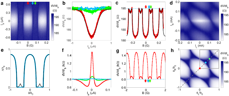
Let us now present the measured at the center of the trijunctions. Due to malfunctioning of the central Au electrode of the 1st device, the data were taken on the 2nd and the 3rd devices. Figure 4a shows the measured on the 2nd device (whose design is identical to the 1st one) as functions of and at an elevated temperature of 0.15 K (such that 0.5). Figure 4b shows the vertical line cuts of Fig. 4a at three different fields indicated by the arrows in corresponding color. And Fig. 4c shows the horizontal line cut of Fig. 4a at =0. Also shown in Fig. 4f and 4g are the and curves, respectively, measured on the 3rd trijunction whose central contact was in the tunneling regime.
It can be seen that with sweeping global magnetic field along the diagonal direction of the flux space (i.e., along the dashed line in Fig. 4h), the minigap at the center of the trijunction varies periodically from open to closed to slightly re-opened. Complete gap-closing takes place near the edges in the bluish regions in Fig. 4h, as evident by the facts that the there reaches the normal-state values represented by the horizontal dashed lines in Fig. 4c and 4g, in an accuracy of 1003% for the 2nd device and 991.3% for the 3rd device. The way that the curves touch the dashed lines is again in sharp peaks (i.e., linear closing), hinting that the underlying mechanism of gap-closing and re-opening is a sign-change process. Up on the gap-closing, the curves become completely flat (the blue curves in Fig. 4b, 4f). Such behaviors are impossible to arise from a trivial Josephson trijunction 32 , in the latter a significant gap-like feature will remain on curves even if the transmission coefficient is as high as 0.9.
To understand why the minigap slightly re-opens between the two peaks/dips in Fig. 4c/g, where complete gap-closing would be expected according to Fu-Kane’s MZM phase diagram, we carried out numerical simulations based on the effective Hamiltonian of chiral Majorana states 5 ; 33 : , where , are the two counter-propagating chiral Majorana states in the junction, the reduced Planck constant, the effective group velocity of the chiral Majorana states, and is the coupling between the two states. The details can be found in the supplementary materials 25 . For trijunctions in the long-length limit, we found that the global magnetic field dependence of minigap follows the blue line in Fig. 4e, supporting that the minigap closes completely in the entire shadowed regions of Fu-Kane’s MZM phase diagram.
Our simulation also reveals that the boundary state at the center spreads slightly to the surrounding junctions. The spreading, hence the coupling to the surroundings, cannot be neglected when the length of the junction is finite, leading to the slight re-opening of the minigap. The spreading/re-opening becomes most significant at the vertexes of the shadowed regions, resulting in the small cusps at on the black line in Fig. 4e. Using the functional form of the minigap represented by this black line, the global field dependence of of the 2nd trijunction can be simulated by using the BTK theory, with the parameters obtained through fitting the red curve in Fig. 4b: eV (eV), =123, =0.931, and =0.25 K. The result of simulation is shown as the black line in Fig. 4c.
By using the two half-turn coils, we further measured the zero-bias of the 2nd trijunction over the entire 2D flux space. The results are shown in Fig. 4d. Due to poor electrical connections to the right half-turn coil, the whole device heated up at high , which smeared out some of the details observed in global field sweeping at lower temperatures. Nevertheless, we can still see that the 2D data of measured at the center is qualitatively different from those measured at the ends (Fig. 3), showing gap-closing over extended regions in phase space. With the same fitting parameters as above and the functional form of the minigap obtained from the lattice-model numerical simulation, the 2D data can be roughly simulated (Fig. 4h). The overall patterns of the measured and the simulated 2D data agree with each other, demonstrating the effectiveness of the MZM phase diagram predicted by Fu and Kane. Besides, both the measured and simulated patterns show that the edges of the MZM regions become curved in flux space, due to the same mechanisms (loop inductance and inter-loop coupling) that cause the warping of the patterns in Fig. 3.
To summarize, we have succeeded in fabricating Josephson trijunctions and controlling the phase differences in the trijunctions with the use of magnetic flux. We observed that the minigap at the center of the trijunctions undergoes complete closing near the edges of the shadowed regions in Fu-Kane’s phase diagram, and gets slightly re-opened in the vicinity of the vertexes of the shadowed regions. We demonstrated through numerical simulation that such re-opening is a finite-size effect of the trijunctions. We also showed that the edges of the shadowed regions, near which the MZM appears at the center of the trijunctions, become curved in flux space when the loop inductance cannot be neglected. These findings provide the necessary details for further braiding MZMs by using sequences of magnetic flux pulses, towards the realization of surface code architectures 23 ; 24 and scalable TQC on TI-based two-dimensional platform.
Acknowledgments We would like to thank L. Fu, F.C. Zhang, X.C. Xie, Q.F. Sun, X.J. Liu, X. Liu, G.M. Zhang, and Z.G. Cheng for fruitful discussions. This work was supported by the National Basic Research Program of China from the MOST grants 2016YFA0300601, 2017YFA0304700, and 2015CB921402, by the NSF China grants 11527806, 91221203, 11174357, 91421303, 11774405, and by the Strategic Priority Research Program B of the CAS grant No. XDB07010100.
References
- (1) A. Y. Kitaev, Annals of Physics 303, 2 C30 (2003).
- (2) S. D. Sarma, M. Freedman, C. Nayak, Physics Today 59, 32-38 (2006).
- (3) C. Nayak, A. Stern, M. Freedman, S. Das Sarma, Reviews of Modern Physics 80, 1083-1159 (2008).
- (4) A. Y. Kitaev, Phys.-Usp. 44, 131-136 (2001).
- (5) L. Fu, C. L. Kane, Phys. Rev. Lett. 100, 096407 (2008).
- (6) A. R. Akhmerov, J. Nilsson, C. W. Beenakker, Phys. Rev. Lett. 102, 216404 (2009).
- (7) K. Law, P. Lee, T. Ng, Phys. Rev. Lett. 103, 237001 (2009).
- (8) R. M. Lutchyn, J. D. Sau, S. Das Sarma, Phys. Rev. Lett. 105, 077001 (2010).
- (9) Y. Oreg, G. Refael, F. von Oppen, Phys. Rev. Lett. 105, 177002 (2010).
- (10) J. Wang, Q. Zhou, B. Lian, S.-C. Zhang, Phys. Rev. B 92, 064520 (2015).
- (11) V. Mourik, K. Zuo, S. M. Frolov, S. R. Plissard, E. P. Bakkers, L. P. Kouwenhoven, Science 336, 1003-1007 (2012).
- (12) M. T. Deng, C. L. Yu, G. Y. Huang, M. Larsson, P. Caroff, H. Q. Xu, Nano lett. 12, 6414-6419 (2012).
- (13) A. Das, Y. Ronen, Y. Most, Y. Oreg, M. Heiblum, H. Shtrikman, Nature Physics 8, 887-895 (2012).
- (14) S. M. Albrecht, A. P. Higginbotham, M. Madsen, F. Kuemmeth, T. S. Jespersen, J. Nygard, P. Krogstrup, C. M. Marcus, Nature 531, 206-209 (2016).
- (15) H. Zhang, C. X. Liu, S. Gazibegovic, D. Xu, J. A. Logan, G. Wang, N. van Loo, J. D. S. Bommer, M. W. A. de Moor, D. Car, R. L. M. Op Het Veld, P. J. van Veldhoven, S. Koelling, M. A. Verheijen, M. Pendharkar, D. J. Pennachio, B. Shojaei, J. S. Lee, C. J. Palmstrom, E. Bakkers, S. D. Sarma, L. P. Kouwenhoven, Nature 556, 74-79 (2018).
- (16) M. Veldhorst, M. Snelder, M. Hoek, T. Gang, V. K. Guduru, X. L. Wang, U. Zeitler, W. G. van der Wiel, A. A. Golubov, H. Hilgenkamp, A. Brinkman, Nat. Mater. 11, 417-421 (2012).
- (17) J. Wiedenmann, E. Bocquillon, R. S. Deacon, S. Hartinger, O. Herrmann, T. M. Klapwijk, L. Maier, C. Ames, C. Brune, C. Gould, A. Oiwa, K. Ishibashi, S. Tarucha, H. Buhmann, L. W. Molenkamp, Nature commun. 7, 10303 (2016).
- (18) H. H. Sun, K. W. Zhang, L. H. Hu, C. Li, G. Y. Wang, H. Y. Ma, Z. A. Xu, C. L. Gao, D. D. Guan, Y. Y. Li, C. Liu, D. Qian, Y. Zhou, L. Fu, S. C. Li, F. C. Zhang, J. F. Jia, Phys. Rev. Lett. 116, 257003 (2016).
- (19) E. Bocquillon, R. S. Deacon, J. Wiedenmann, P. Leubner, T. M. Klapwijk, C. Brune, K. Ishibashi, H. Buhmann, L. W. Molenkamp, Nature nanotech. 12, 137-143 (2017).
- (20) Z. Lyu, Y. Pang, J. Wang, G. Yang, J. Fan, G. Liu, Z. Ji, X. Jing, C. Yang, F. Qu, L. Lu, Phys. Rev. B 98, 155403 (2018).
- (21) S. Nadj-Perge, I. K. Drozdov, J. Li, H. Chen, S. Jeon, J. Seo, A. H. MacDonald, B. A. Bernevig, A. Yazdani, Science 346, 602-608 (2014).
- (22) S. Vijay, T. H. Hsieh, L. Fu, Physical Review X 5, 041038 (2015).
- (23) D. Litinski, M. S. Kesselring, J. Eisert, F. von Oppen, Phys. Rev. X 7, 031048 (2017).
- (24) See online supplementary materials.
- (25) H. J. Kwon, K. Sengupta, V. M. Yakovenko, Euro Phys. J. B - Cond. Mat. 37, 349-361 (2003).
- (26) C. W. J. Beenakker, Three ”Universal” Mesoscopic Josephson Effects. Transport phenomena in Mesoscopic Systems, H. Fukuyama and T. Ando, eds. Springer, Berlin (1992).
- (27) G. E. Blonder, M. Tinkham, T. M. Klapwijk, Phys. Rev. B 25, 4515-4532 (1982).
- (28) A. Barone, Physics and application of the Josephson effect, John Wiley and Sons, Inc. (1982).
- (29) H. le Sueur, P. Joyez, H. Pothier, C. Urbina, D. Esteve, Phys. Rev. Lett. 100, 197002 (2008).
- (30) G. H. Lee, S. Kim, S. H. Jhi, H. J. Lee, Nature commun. 6, 6181 (2015).
- (31) C. Padurariu, T. Jonckheere, J. Rech, R. M lin, D. Feinberg, T. Martin, Y. V. Nazarov, Phys. Rev. B 92, 205409 (2015).
- (32) A. C. Potter, L. Fu, Phys. Rev. B 88, 121109 (2013).
See pages ,- of SM.pdf