Impact of single and double oxygen vacancies on electronic transport in Fe/MgO/Fe magnetic tunnel junctions
Abstract
The combination of a low tunnelling barrier height and a large tunnelling magnetoresistance (TMR) ratio in MgO-class magnetic tunnel junctions has enabled next-generation information storage and bio-inspired computing solutions thanks to the spin transfer torque effect. Recent literature has proposed that this synergistic combination arises from the electronic properties of oxygen vacancies. To explicitly understand their impact on spin-polarized transport, we have computed the electronic and transport properties of single (F centers) and paired (M centers) oxygen vacancies using density functional theory and the projector augmented wave (PAW) method. These point defects can generate barrier heights as low as 0.4V for FeCo electrodes irrespective of the defect’s spatial position within the barrier, and of the orientation of the M center. These defects promote a strong decrease in the conductance of the spin up channel in the MTJ’s parallel (P) magnetic state that mainly accounts for an order-of-magnitude drop in TMR, from 10000% in the ideal case toward values more in line with experiment. When placed in the middle layer of the MgO barrier, the F center introduces additional P transmission away from the point. This scattering lowers TMR to 145%. In contrast, the M center merely broadens this transmission around , thereby boosting TMR to %315. Rotating a M center so as to partly point along the transmission direction sharpens transmission around , further increasing TMR to 1423%. When these defects are placed at the MTJ interface, the transmission and ensuing TMR, which reaches 4000%, suggest that such junctions behave as would an ideal MTJ, only with a much lower barrier height. Our results thus theoretically reconcile the concurrent observations of high TMR and low barrier heights, in line with experimental preparation techniques such as post-deposition oxidation of metallic Mg, which can generate oxygen vacancies at the lower MTJ interface, and annealing which can promote M centers over F centers. Our theory is also in line with an origin of perpendicular magnetic anisotropy in terms of oxygen vacancies at MTJ interfaces. The effective size of these vacancies sets a limit for both the barrier thickness, in line with experiment, as well as for the MTJ’s lateral dimension. Our work provides a much-needed theoretical basis to move beyond the mostly unsuspected, fortuitous defect engineering of spintronic performance that has thus far propelled MgO-based spintronics and its applications.
pacs:
71.15.Mb, 73.20.-r,73.40.-c,73.40.QvI Introduction
Spintronic research exploits both charge and spin degrees of freedom in solid-state systemsŽutić et al. (2004); Makarov et al. (2016); Lu et al. (2016); Peng et al. (2014). A widely studied spintronic device is the magnetic tunnel junction (MTJ), composed of two ferromagnetic metallic electrodes separated by an ultrathin dielectric. The electrical resistance of the MTJ depends on the relative orientation of the electrode magnetizations, which can be controlled by an external magnetic field or a spin-polarized currentLocatelli et al. (2013). This change in resistance is called tunnelling magnetoresistance (TMR) and is defined as
| (1) |
where and are the resistances for parallel (P) and antiparallel (AP) configurations of the two magnetizations of the electrodes.
Initial MTJs with an Al2O3 tunnel barrier exhibited a maximum TMR of 70% at room temperature.Moodera et al. (1995); Wang et al. (2004) Theoretical studies of magnetotransport across Fe/ZnSe/FeMacLaren et al. (1999) and Fe/MgO/FeMacLaren et al. (1999); Butler et al. (2005); Butler (2008); Zhang and Butler (2003); Butler et al. (2001a) MTJs revealed that the TMR can be greatly increased if the amorphous barrier is replaced by a crystalline one, such that certain orbitals with a high spin polarization in the electrodes preferentially tunnel across the barrier. Nowadays, textured FeCoB/MgO/FeCoB MTJs with TMR values above 600% at room temperature Ikeda et al. (2008) offer promising prospects for data read-out, storage and processing, magnetic sensorsKent and Worledge (2015); Chappert et al. (2007); Ikeda et al. (2007).
Despite the importance of these MTJ technologies, an understanding of exactly how the device operates remains a work in progress. Indeed, the TMR effect is a complex phenomenon that depends strongly on the electronic structure of the electrodes, the properties of the insulating barrier and on the chemical bonding at the MTJ interface. As an illustration, consider how the success of achieving high TMR concurrently with low barrier heights requiredHalisdemir et al. (2016) to implement spin transfer torque toward these MTJ technologiesKent and Worledge (2015); Chappert et al. (2007); Ikeda et al. (2007); Locatelli et al. (2013) imply that structural defects, which may lower TMR from the 10000% theoretical prediction, may actually play a beneficial spintronic role here.
Several causes for an effective deviation from the MTJ’s ideal structure have been considered. Experiments often reveal the presence of interface oxidation, which alters the nature of chemical bonding at the interface between the ferromagnetic electrodes and the MgO spacer and can degrade TMRMeyerheim et al. (2001). The combination of theoreticalZhang et al. (2003) and experimentalBonell et al. (2009) studies showed that, even if one includes the interface disorder or the oxidation of interfacial Fe layer, the drastic drop of TMR cannot be fully explained by this mechanism alone.
As another cause, atomic diffusion may occur during the sample preparation and annealingHayakawa et al. (2006). In particular, boron diffusion into the MgO barrier (forming boron oxides), or its segregation at the CoFe/MgO interface, has been studiedMiyajima et al. (2009); Kozina et al. (2010); Pinitsoontorn et al. (2008); Rumaiz et al. (2011), but this is not always the case Kurt et al. (2010); Mukherjee et al. (2015); Wang et al. (2016). Rather, at a proper annealing temperature, boron does not diffuse into MgO but rather goes further away from the interfaces. Even if boron diffuses into MgO, it was shown theoretically that this should not create additional states within the MgO band gap Bai et al. (2013).
Finally, another source can be imperfections in the MgO spacer itself, such as grain boundaries and point defects. The impact of the grain boundaries on the electronic structure and on the transport is difficult to address. Nonetheless, it was shown by Mizuguchi et al.Mizuguchi et al. (2007) that the tunnelling current flows uniformly despite the existence of the grain boundaries and hence the device performance is not affected considerably by this kinds of defects. Moreover, the combined experimental and theoretical investigations of Bean et al.Bean et al. (2017) showed that grain boundaries can cause a decrease of the effective barrier of MgO but this band gap decrease can not explain the observed low barrier heightsSchleicher et al. (2014).
Point defects, on the other hand, can promote localized states within the band gap of MgO, giving rise to a variety of interesting optical, catalytic and transport properties that are absent in the ideal crystalline materialRosenblatt et al. (1989). The most plausible imperfections are oxygen and magnesium vacancies, denoted F and V centers respectively. They can appear in a neutral, singly charged or doubly charged state that is denoted as F+, F2+, V- V2-, respectively. Moreover, two point defects can form a paired vacancy: two F centers form a F2 pair of oxygen vacancies, which is a M center when they are nearest-neighbor on the oxygen sublattice. A F center can also combine with a V center to form a MgO vacancy.
As discussed by Gibson et al.Gibson et al. (1994), oxygen vacancies exhibit the lowest formation energy, which implies that this species of defects is more likely to occur in MgO. This defect species promotes localized states in the band gap of MgO and can affect the optical and the electrical properties of the dielectric Gibson et al. (1994); Velev et al. (2007); Velve et al. (2007); Schleicher et al. (2014). As a result, the barrier heights encountered by the propagating electrons are locally reducedKim et al. (2010); Studniarek et al. (2017). The electrons can then tunnel through the barrier via these additional states with different scattering rates than those for an ideal barrier. This would explain experimental reports of a barrier height in MgO MTJs that is far below the nominal value of 3.9 eV (see Tab. 1).
| MTJ | TMR () | Barrier height (eV) |
|---|---|---|
| Fe/MgO/Fe | 130 (1901K) | 0.38/0.82Miao et al. (2008) |
| Fe/MgO/Fe | 180 (24720K) | 0.39Yuasa et al. (2004) |
| FeCo/MgO/FeCo | 120-220 | 1.1-1.7 Parkin et al. (2004) |
| FeCoB/MgO/FeCoB | 100 | 0.62/0.5Schleicher et al. (2014) |
| Fe/MgO/FeCo | 234.2K/ 2070K | 0.9Mitani et al. (2003) |
Although oxygen vacancies within MgO appear to play an important role not only toward MTJ performance, but also spin transfer torqueHalisdemir et al. (2016), their clear identificationLu et al. (2009); Teixeira et al. (2011) and impact on the tunnelling current has remained a work in progress. According to theory,Velve et al. (2007); Velev et al. (2007); Ke et al. (2010) single oxygen vacancies should create barrier heights of about 1.1 eV for the tunnelling electrons and decrease the resulting TMR. Even if we consider more F-type vacancies within MgOKe et al. (2010), the general conclusion is that these vacancies should degrade the TMR ratioMiao et al. (2008). On the other hand, in the presence of a 0.4eV barrier height, coherent transport seem to be spintronically favorableYuasa et al. (2004); Schleicher et al. (2014); McKenna and Blumberger (2012). Indeed, it was suggested by Schleicher et al. Schleicher et al. (2014) that this barrier arise from M centers, which preserve coherent transport according to McKenna and BlumbergMcKenna and Blumberger (2012). Only recently has a unified experimental/theoretical picture of the potential landscape due to F and M centers emergedTaudul et al. (2017); Schleicher et al. (2018).
In this work, we study the electronic properties of F and M centers in MgO, and their impact on spin and symmetry polarized transport in Fe/MgO/Fe junctions employing density functional theory. The transport is calculated within the Landauer-Büttiker formalism as implemented in PWcond Smogunov et al. (2004). We show that the position of defect levels with respect to the Fermi level of the MTJs is robust against the type of exchange and correlation functional, and do not depend on the defect’s spatial position in the barrier. Our results indicate that M centers can account for the experimental barrier height of 0.4 eV, and promote improved TMR relative to F centers. We also find that the defect’s position within the barrier thickness strongly conditions spintronic performance. Relative to an ideal MTJ, this performance is mostly unaffected when the F or M center is close to an interface, but is reduced when the vacancy is moved onto the barrier’s middle monolayer. In that case, rotating the M center restores stronger TMR. When judicious, we discuss how our theoretical framework of spintronic tunnelling across MgO in the presence of F and M centers adheres to experiment. The spatial extent of the F and M center suggest that a MTJ with a lateral size 2nm can still exhibit high TMRTaudul et al. (2017).
The paper is organized as follows: In section II we present the details of our calculations and methodology. In sec. III we compute and discuss the electronic ground state properties of F and M centers either in bulk MgO or incorporated into MTJs. We compare the defect level positions obtained theoretically with the experimental data and discuss its change with respect to the types of electrodes. In sec. IV we show the results of transmission calculations for Fe/MgO/Fe MTJ with oxygen vacancies generated within MgO spacer. We explain the importance of the geometrical position of the vacancy with respect to the interface and the orientation of the defect plane for the M center. In the last section, we conclude the paper with a general discussion.
II Methodology
II.1 Ground state calculations
To calculate the electronic structure of MgO with F and M centers, denoted as F(M)-MgO, we created the F/M centers by removing one/two neutral oxygen atoms from a simple cubic supercell containing 64 atoms. We used the experimental MgO lattice constant of Å. These calculations were performed using VASP package Kresse and Furthmüller (1996); Kresse and Joubert (1999) based on the projector augmented wave (PAW) methodBlöchl (1994) and the Pedrew, Burke, Enzerhof (PBE) generalized gradient approximationPerdew et al. (1996) for the exchange-correlation potential. The kinetic energy cutoff value of 500 eV for the plane wave basis set and the convergence criterion for the total energy of 1eV is used. The structures with defects were relaxed by requiring that the forces acting on atoms be less than 0.001 eV/Å. Due to the large size of the supercell, we found that a -point mesh of 444 using the Methfessel-Paxton method with a smearing of eV yields a satisfactory convergence of localized states resulting from these defects. Since it is well known that the generalized gradient approximation (GGA) underestimates the size of the band gap, we also used the hybrid Heyd, Scuseria, Ernzerhof (HSE) functionalPaier et al. (2006) to correct the band gap and verify whether the defect level positions with respect to the Fermi level depends on the type of functional employed. The HSE hybrid functional mixes a portion of exact Fock exchange with that of DFT using an adjustable parameter . We found that, by increasing the Fock exchange to 43% in HSE06, we can reproduce the experimental band gap of MgO. This parameter is then used to calculate the defect levels in the MgO MTJs employing HSE06.
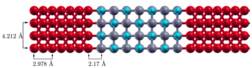
To determine the positions of the defect levels with respect to the Fermi energy and compare them with experiment, we used more realistic Fe/MgO/Fe MTJs. At the metal/insulator interface, the electronic transfer between the two materials and the metal induced gap states (MIGS) in the band gap of MgO will peg the Fermi level position for the junction and establish the energy position of the defect levels accordingly. The geometry of the MgO/Fe supercell was based on the experimental results: the Fe conventional unit cell was rotated by a 45∘ with respect to that of MgO to match the lattice constants of both materials and avoid strains in the structure: . In addition, oxygen atoms were placed on top of Fe atoms and the Fe-O distance at the interface was fixed to 2.17 Å following previous theoretical predictionsButler et al. (2001b); Velev et al. (2007). It is important to notice that the measured Fe-O distance is in the range of 2 ÅUrano and Kanaji (1988); Wulfhekel et al. (2001) to 2.2 ÅMeyerheim et al. (2001). We fixed the lattice constant of MgO ( = 4.21 Å) and adjusted the lateral lattice parameter of the electrodes to it. This choice reflects the experimental evidenceHayakawa et al. (2005) that the annealing of FeCoB/MgO-based MTJs led to a recrystallization of the electrode/barrier interfaces so as to adopt the MgO lattice constant. The lattice parameter along the axis was rescaled accordingly. The structure of the junction and relevant parameters are indicated in Fig. 1.
The experimental FeCoB electrodes are initially amorphous alloys whose interface with MgO adopts the latter’s (001) texture upon annealingHayakawa et al. (2005). However, the exact arrangement of Fe and Co atoms is not really known. Moreover, the role of boron or its influence on the electronic structure of FeCo electrode is not clear. Therefore in our work we decided to consider a simplified scenario in which the FeCo electrode has the same structure as that of Fe. For the FeCo/MgO calculations, we have alternated the Fe and Co layers and chosen Co at the interface with MgO. Nonetheless, even the simplified structure can give us some insights into the impact of the type of electrode on the defect levels.
For the calculations involving full junctions, the kinetic energy cutoff value and the convergence criterion were the same as for the bulk MgO, but the value of was decreased to 0.1 eV and the spin polarized version of PBE-GGA was used. To compute the electronic structure of oxygen vacancies, the lateral directions of MTJ were doubled and periodic boundary conditions applied in all directions.
II.2 Transport calculations
The ballistic conductance is calculated using Landauer-Büttiker Landauer (1987); Büttiker et al. (1985) formula
| (2) |
where is the total transmission at the Fermi energy and the summation is over all bands crossing the , for each point and spin . The electron transmission was evaluated using the scattering based approach with a plane wave basis set and ultrasoft pseudopotential (USPP) scheme as implemented in the PWcondSmogunov et al. (2004) module of the Quantum Espresso (QE)Giannozzi et al. (2009) package.
The conductance was evaluated between two semi-infinite electrodes connected by a scattering region that contains an insulating MgO spacer and a part of the leads on each side of the spacer. To compute the electron transmission at a given energy E, we first calculated the total energy of the ground state properties with the PWscf code from QE packageGiannozzi et al. (2009) and determined the effective potential. We then constructed the generalized Bloch states, including propagating and evanescent states, as a solution of Kohn-Sham equations at energy E for the infinite periodic leads, and the results were used to construct the scattering states and compute the transmission across the entire system. Moreover, in the spin density functional picture, electrons of different spin move independently in their different self-consistent potentialsSmogunov et al. (2004). Therefore in this approach spin flip events are not included and the total transmission is the sum of the two spin channels such that .
To find how many electrode layers should be contained in the scattering region, we studied the changes of the electrostatic potential in the scattering region. To ensure that the electron wave function changes smoothly at the interface between the bulk of the electrode and the scattering region, the part of the leads in the scattering region has to be big enough so that the changes induced in the electrostatic potential due to the interaction with MgO are contained entirely within the scattering region. If not, an artificial potential that scatters the incoming electrons could be present and might affect the results. By comparing the total electrostatic potential for the scattering region to the total potential of the bulk electrode, we found that from the 2nd-3rd monolayer (ML) of Fe, the bulk electrostatic potential is restored. In order to guarantee a proper geometrical matching between the scattering region and the electrodes, we used 4 ML of Fe on the left side of MgO and 5 ML of Fe on the right side. For the defect calculations, we doubled the lateral size of the junctions. When the antiparallel alignment of the electrodes was considered, the size of the junction along the direction was doubled, such that the composition of the supercell was Fe(P)/MgO/Fe(AP)/MgO/F(P).
In the ground state calculations with PWscf code, the cutoff energy values for the plane wave basis set and the electron density were set to 40 Ry and 400 Ry, respectively. The electronic occupations were broadened using a Gaussian smearing technique with a smearing parameter =0.02 Ry. The total energy convergence threshold was set to 10-8 Ry and the electron density mixing parameter to 0.1. For the ground state calculations of the ferromagnetic alignment of the electrodes, we used a k-point mesh of 551, while for the antiferromagnetic alignment the same k-point grid was slightly shifted out of the point in order to speed up the convergence. Since we needed to use the same form of the pseudopotential and corresponding exchange-correlation functional for all atoms in the junction, we chose the Perdew and Wang (PW91) generalized gradient functional Perdew and Wang (1992) in a spin-polarized form already generated and available in the QE library.
An important factor in the transmission calculations is the convergence of the 2D basis set used in the PWcond. Here, two parameters control the basis set: (i) ewind defines the energy window for reducing the 2D plane wave basis set in the transverse plane, and (ii) epsproj is a threshold for the 2D basis set reduction. The default values for the two are and . Generally, the larger ewind and the smaller epsproj are, the higher the accuracy of the calculations is. However, the increase in the transmission accuracy increases the computational cost and a suitable compromise should be found. These parameters were tested by examining the complex band structure (CBS) of bulk Fe and MgOVelev et al. (2005); Bowen et al. (2006). We found that were sufficient to convergence the CBS and therefore were used also to compute the transmission. In addition, the transmission was evaluated as a function of the number of points in the 2D BZ. We tested meshes of 2020, 3030, 5050 and 8080 k-points and kept the 5050 which showed a well-converged transmission.
III Electronic structure
III.1 MgO bulk
Here, we briefly describe the ground state electronic properties of M center within MgO bulk and MgO incorporated in the Fe(FeCo)/MgO MTJs. The removal of two neighboring oxygen atoms from an MgO supercell results in the creation of two occupied energy levels below . The electrons that were transferred from Mg and remain after the oxygen removal are trapped and are mostly localized on the vacancy sites. Since the electron distribution on the vacancies resembles that of an oxygen O2- ion, the atoms around the defect are only slightly distorted. The resulting alteration to the resulting electronic structure is very slight, such that the distortion was neglected.
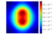
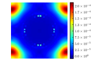
To understand the nature of the M center levels, we plot in Fig. 2 the orbital-projected band structure and the density of states (DOS) for MgO containing a M center (M-MgO). The valence states of MgO are mostly of O character while the conduction states comprise Mg and -like states. The defect levels show mostly contributions form -like orbitals with a smaller part coming from -like states. By projecting the DOS on Mg and O sites, we found that the M-levels are the results of a hybridization between O orbitals and both Mg and states. The contribution of -like states is much smaller and can be neglected. Note that the small dispersion around the point is a result of an artificial interaction between the periodic images of the M centers due to the 64-atom size of our supercell. As we showed elsewhereTaudul et al. (2017), for supercells with 216 atoms, these levels exhibit no energy dispersion. This means that the defects are well separated from each other and spatially localized. Nonetheless, the dispersion observed for a 64-atom supercell does not significantly change the level positions, and as such it can be neglected.
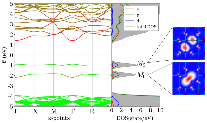
We plot as insets to Fig. 2 the electronic spatial distribution for each of the M centers ground states. It is clear that the electron distribution for the M1 state resembles a bonding-like state, while it is anti-bonding for the M2 state. As in the case of bond formation between atoms, the coupling between two F centers creates a bonding state with a lower energy, and an anti-bonding state with higher energy, with respect to the original F state energy level. Indeed, the F center peak is always positioned in between two M center ground states. As a consequence, the barrier height created by the F center is always higher than that associated with the M2 state.
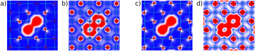
Figure 3 presents the spatial distribution of the electron density for both the ground (panels a/c) and excited (panels b/d) states of M-MgO. In panels a/b (c/d), a 214-atom (62-atom) supercell was used. We observe how neighboring oxygen vacancies hybridize to create an M center. As expected from the band structure plots, the electrons remaining after oxygen removal are localized on the vacancy sites and the electrons are distributed among the vacancies. Since the M center’s excited state lies within the conduction band states, a nonzero electron density is present on atoms far from the defect. The electron density plots also reveal a hybridization between the M center states and the nearest oxygen ions, thereby showing that the defect level’s excited state is indeed mostly of oxygen character. The spatial electron density of the M center is fully isolated from the periodic images in the 214-atom supercell. Thus, the lateral extent of the M center spans 1 ML on either side of the oxygen vacancy sites that define the M center. On the other hand, spatial overlap develops between the electron density of M centers in the 62-atom supercell calculation. This means that M centers separated by 2 ML of MgO will experience electronic interactions. The electron distribution also indicates that the ground states of the M center are mostly s-like, while the excited states are of p-like character.
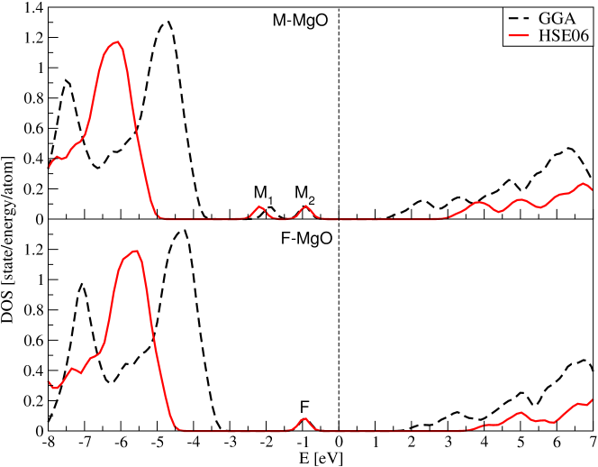
The results presented above are obtained within the GGA functional, which is known to underestimate the band gap. Therefore, as discussed in the methodology section, we also employed the HSE06 hybrid functional to accurately determine the defect level positions within the MgO band gap. Figure 4 presents the results of GGA and HSE06 bulk calculations for both M-MgO and MgO containing a F center (F-MgO), with 0 eV. For both F-MgO and M-MgO, compared to the GGA results, the hybrid functional causes a shifting of the valence and the conduction bands towards lower and higher energies, respectively. The hybrid functional, due to the inclusion of a portion of the exact Fock exchange which is orbital dependent, increases the localization by reducing the self-interaction error appearing in GGA. This fact has almost no influence on the F state position since it is a single localized level. However, in the case of a M center, where two additional energy levels are created in the MgO band gap, the difference can be noticeable and we observe a slight shift of the M1 state further away from the M2 level. This difference of the position between the GGA and the HSE06 calculations is about 0.27 eV. Nonetheless, aside from the shift in the M1 energy position, we otherwise obtain a similar energy dependence of the DOS. This shows how less intensive GGA-based calculations already yield a qualitatively correct picture of the electronic properties of oxygen vacancies in MgO. It is worth noticing that the defect levels are placed near the middle of the MgO band gap irrespective of the type of functional used.
III.2 M-MgO/Fe(FeCo) junctions
We now calculate the electronic structure of both Fe/MgO/Fe and FeCo/MgO/FeCo junctions with oxygen vacancies in the MgO spacer layer. Fig. 5 presents the DOS projected on MgO(7ML) layers with F/M center generated in the middle 4th layer of the MgO spacer. Due to the contact with the metallic electrode, MIGS appear in the MgO band gap and decay with the number of MgO layers. As a result the band gap of MgO disappears at the interface because of states coming from Fe. From the third layer the band gap of a bulk MgO is restored. Moreover, the ferromagnetic electrode induces spin polarization in the neighboring MgO layers and the difference in the DOS of spin up and down electrons can be clearly seen.
For the Fe/MgO heterostructures, the M1 and M2 states are located respectively at -1.7 eV and -0.7 eV below the Fermi level, while the F center level is at -1.2 eV. As expected the barrier height associated with the F center is in between the M2 and M1 levels. In the case of the FeCo electrodes the defect levels are shifted towards the Fermi level by about 0.5 eV. It is worth noticing that not only are defects levels shifted, but also the whole band structure of MgO is rigidly shifted towards higher energies. This shift can be understood considering the 0.5 eV difference in the work function between Fe and Co. As before, the vacancy affects also the closest MgO layers up to 3 ML of MgO along the direction perpendicular to the M-center plane.
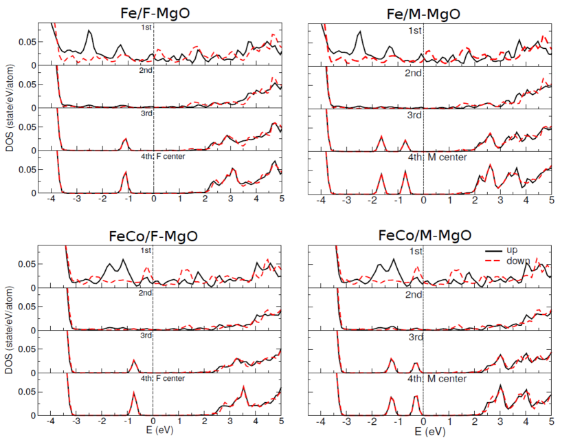
We also studied the effect of shifting the M center within the MgO (7 ML) spacer and found that the defect energy level remains practically unchanged when the vacancy approaches the interface (data not shown)Taudul (2017). However, if the vacancy is placed on the interfacial MgO layer the DOS associated with the F/M center is washed out due to the strong interaction with the ferromagnetic electrode. Clearly, when the defect is closer to the interface, the hybridization between the two types of materials is strongly affected, which in turn influences the position of the Fermi level. However, it is surprising that this modification led only to a small differences in the Fermi level positions of the order of 0.09 eV.
Thus far, we have considered only the situation where the M center is in the plane parallel to the interfaces. In that case, we found that the effective size of the M center in the direction perpendicular to the interface reaches up to 3 ML of MgO due to charge transfer onto adjacent MLs. We can also rotate the M center such that it be partially aligned along the direction and shared between two neighboring MgO layers. In that case, the effective M center size reaches 4ML. Regardless of the orientation of the defect plane, the level position of the M center remains practically unchanged and similar results for the DOS are also obtained (not shown)Taudul (2017). Even though the changes in the DOS upon shifting or rotating the M center within the MgO spacer are not significant, we will show later that these changes have a huge impact on the transmission as hinted by complex band structure calculations(Taudul et al., 2017). Thus, based on our calculations, we can state that the computed energy range for barrier heights associated with an M center can be associated with those measured experimentally at 0.4 eV, due to the M2 state located 0.4 eV below the Fermi level for a FeCo/MgO/FeCo MTJ.
IV Ballistic transport
IV.1 Ideal MgO-based junctions
We first calculated the transmission at the Fermi level for junctions with an ideal, 5 ML-thick MgO structure in order to examine the impact of introducing oxygen vacancies. The results found for the 7 ML spacer are similar to these for 5 ML and will be only briefly discussed.
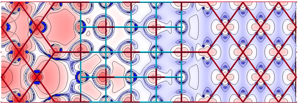
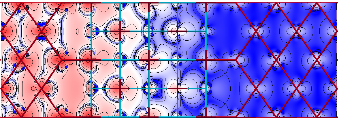
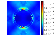
Fig. IV.4 presents the transmission in the two dimensional Brillouin Zone (2D BZ) for the parallel electrode magnetization for the spin up and the spin down electron channels (left and middle panels) and the corresponding transmission for the antiparallel configuration (right panel). In agreement with previous theoretical predictions Mathon and Umerski (2001); Butler et al. (2001b), we found that the majority electron transmission is centered around the point and dominated by the symmetry. The transmission for the minority channel occurs basically at the edges of the 2D BZ and is much smaller than for the majority channel. The transmission in the AP configuration is a mixture of features seen in both spin channels.
 |
 |
 |
| (a) | (b) | (c) |
By summing the transmission over the BZ for each channel, we obtain the conductance (see eq. 2) and the resulting TMR. Tab. 2 summarizes the transmission results for junctions with 5 and 7 ML of MgO. As expected, the transmission decays exponentially with the thickness of the MgO spacer and hence drops by at least one order of magnitude when passing from 5 to 7 ML of MgO and the TMR increases with the number of MgO layers. This reflects the favorable symmetry filtering across MgO(001) of electrons with a high spin polarization at the bcc(001) Fe electrodes’s Fermi level. For this reason, the channel is blocked in the MTJ’s AP magnetic state, such that transmission is ensuring by and symmetry channels, which appear for both spin populations at in Fe. When the MgO thickness is increased, the contributions to the conductance from the strongly attenuated and channels become smaller. This leads to a bigger overall difference in the transmission between the P and the AP configurations and causes the increase in TMR. According to literatureKe et al. (2010), the TMR value should continue to grow up to 13 ML of MgO due to the the dominant contribution. After exceeding this thickness, the TMR will also start to decrease due to the exponential decay of the tunnelling current.
IV.2 F/M center in the middle layer of MgO
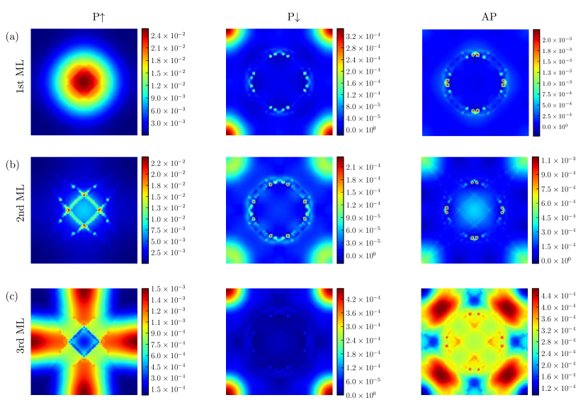
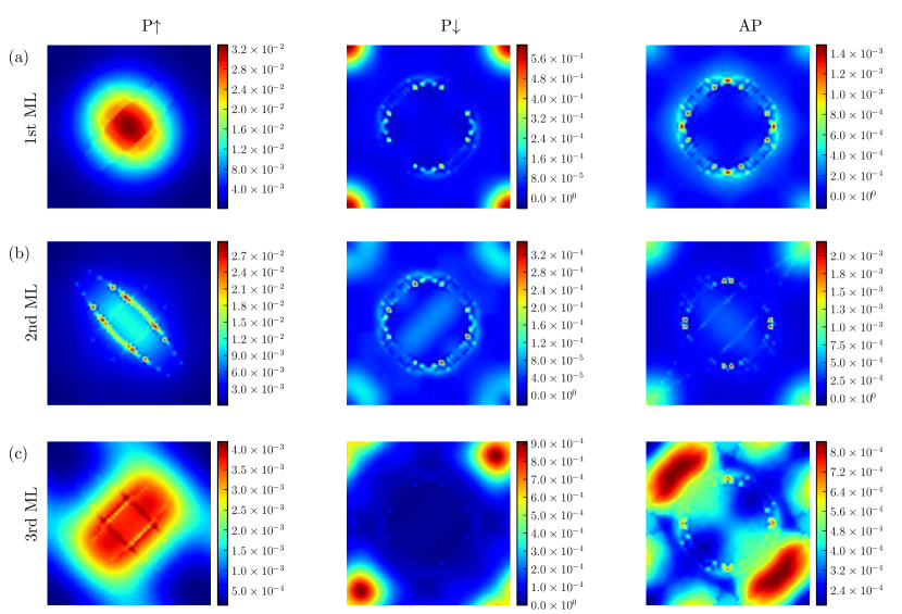
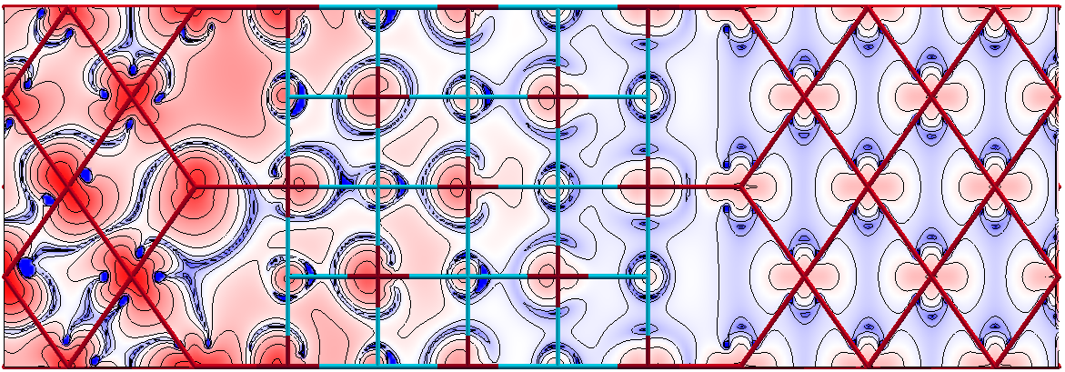
In the next step, we introduced single and double oxygen vacancies in the middle layer of the MgO spacer. First, the M center’s two oxygen vacancies were placed within the middle layer. Fig. 7(c) and 8(c) show the corresponding 2D BZ transmission for F and M centers, respectively. The BZ transmission distribution for P spin electrons is only slightly affected by the presence of the vacancies, resulting in a small increase in the total amplitude with respect to the ideal case (see Table 2). However, in the spin channel, a clear distinction in the P transmission between the F and the M centers can be made. It appears that the F center scatters the propagating electrons to states with higher -vectors. As a result, the transmission has a minimum at the point and occurs mostly along and directions with maxima at the edges of the 2D BZ. The electrons are scattered symmetrically in each direction due to spherical symmetry of a single oxygen vacancy. On the other hand, the P spin up transmission in the presence of the M center becomes broadened in the 2D BZ but maintains a symmetric maximum at the vicinity of the point. This clearly suggests that, while the transmission across a F center is reduced by an order of magnitude due to transport across k states, coherent transport that preserves spin and symmetry of the electron wave function is still possible when M center is present in the MgO spacer.
We find that, while F and M centers promote a reduction in total Pup transmission (see Tab. 2), both centers promote an increase in both the Pdn and AP total transmissions. Furthermore, the transmission distribution in the AP configuration changes significantly from that of an ideal MgO junction (see Fig. IV.4). While introducing defects reduces the TMR, the TMR is higher for M centers compared to F centers. We found similar trends for the 7 ML , (see Tab. 2). Again, if we increase the number of MgO layers (here from from 5 to 7 ML), the TMR also increases regardless of the defect type.
| P-UP | P-DOWN | AP | TMR [%] | |
|---|---|---|---|---|
| 5 ML | 79.0 | 0.46 | 1.0 | 7850 |
| F (5ML) | 7.21 | 0.63 | 3.2 | 145 |
| M (5ML) | 17.1 | 1.47 | 4.5 | 315 |
| 7 ML | 5.3 | 0.003 | 0.03 | 15770 |
| F (7ML) | 0.12 | 0.006 | 0.03 | 304 |
| M (7ML) | 0.62 | 0.007 | 0.04 | 1624 |
Since the M center promotes a 0.4eV barrier height in MgO MTJs with FeCo electrodes, these transmission results can account for the simultaneous experimental occurrence of high TMR alongside 0.4eV barrier heights. They also confirm the initial assumption that coherent transport can be preserved when a M center is present. Note that the defect level positions discussed previously were evaluated using the VASP code with the PAW basis set. To verify the robustness of these results, we switched to a plane wave basis set in conjunction with an ultrasoft pseudopotential approach. While the shape of the layer-projected DOS is practically the same, we noticed a small shift of about 0.15 eV of the F and M1 states towards lower energies. We then examined how this shift can influence the conductance by examining the transmission in the energy window eV. In the case of the spin up transmission, the 2D BZ distribution and the amplitude of the transmission for all structures remains practically the same. However, some changes were observed in the spin down transmission. The likely cause is the presence of minority interfacial resonant states (IRS)Butler (2008). This discrepancy should not influence the generality of the results presented since the contributions from the spin down channel to the are much smaller than those of the spin up channel.
IV.3 Effect of shifting the vacancy on the transmission
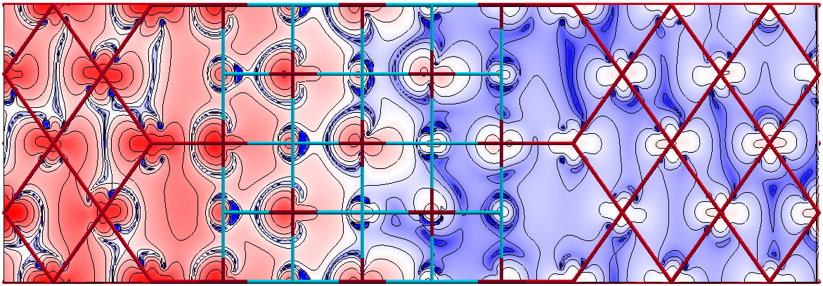
We now examine the impact on spin-polarized transmission of varying the position within the barrier of the F and M centers alters. Although we did not observe any significant change in the layer-projected DOS upon moving the vacancy to the interface, the transmission was nevertheless profoundly altered.
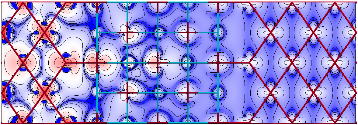
Fig. 7(a) and 8(a) respectively show the 2D BZ spin-dependent transmissions with F and M centers generated in the interfacial MgO layer. Here, the M center always remains in the plane parallel to the interfaces. Interestingly, we found that the transmission distribution is almost the same as for the ideal junction with the peaks amplitude very close to the ideal case (compare with Fig. IV.4). The calculated TMR reaches about 4261% and 3911% for the F and M center, respectively, i.e. are of the same order of magnitude as for the ideal junction (see Tab. 3).
| P-UP | P-DOWN | AP | TMR [%] | |
|---|---|---|---|---|
| F in 1st ML | 54.5 | 0.4 | 1.26 | 4261 |
| F in 2nd ML | 20.3 | 0.4 | 1.55 | 1239 |
| F in 3nd ML | 7.21 | 0.63 | 3.2 | 145 |
| M in 1st ML | 67.6 | 0.6 | 1.70 | 3911 |
| M in 2nd ML | 30.3 | 0.5 | 2.49 | 1135 |
| M in 3nd ML | 17.1 | 1.47 | 4.5 | 315 |
When vacancies are on the second layer from the interface, the transmission decreases and we observe additional sharp spikes in the P spin up channel (Figs. 7(b) and 8(b)). The P spin down and AP transmission distributions are only slightly affected. Note that the layer alternation also causes a rotation of the M center within the plane when we go from one layer to the next one. This explains the observed rotation in the transmission amplitude in the 2D BZ (compare for example panel (c) and (d) in Fig. 8).
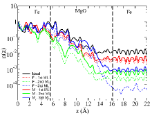
To understand the changes in the transmission when varying the F/M centers position, we analyzed a real space distribution of scattering states at the point. We discuss here the MTJ’s P magnetic state, focusing on the spin up channel since its transmission strongly drives the ensuing spintronic performance. In the spin up channel we focus on the symmetry since is has the smallest attenuation rate within MgO barrier and the biggest impact on the resulting transmission. Fig. 9 shows the density of a scattering state, summed over the plane, as a function of the position along the transport direction for various defect configurations. Clearly, in the presence of vacancies, the amplitude of the channel is decreased with respect to the ideal case. Interestingly, M centers systematically yield a higher transmission amplitude than F centers at all defect positions within the barrier.
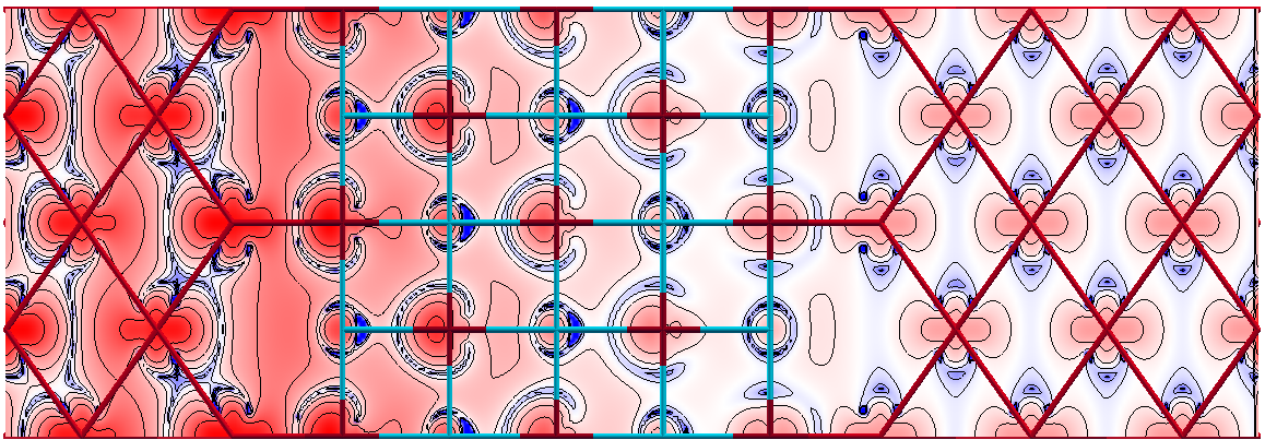
Fig. 10 shows the scattering states at the Fermi level across a Fe/MgO(5ML)/Fe junction for the ideal case and the various positions of the F and M centers. All the data are normalized and the same logarithmic scale is used for comparison purposes.
As expected, in the case of an ideal junction, the channel originates from the left electrode, crosses the MgO barrier and ends in the right electrode. When F/M centers are introduced, the distribution of the state changes and depends on the vacancy type and position. The most beneficial configuration is with the vacancies located at the interfacial MgO layer. In that case, the amplitude of the scattering stated is just slightly lowered with respect to the ideal situation, and the channel is still transmitted from the left to the right electrode. Moreover, these graphs indicate that the further from the interface a vacancy is, the bigger the difference between F and M centers. The difference in distribution of the channel for F and M center in the third layer of MgO (Fig. 10) can explain the resulting values of TMR, 145% and 304% respectively, which underscores the synergistic spintronic role of M centers compared to F centers.
 |
|
| (a) Ideal MTJ | |
 |
 |
| (b) F in 1st ML | (c) M in 1st ML |
 |
 |
| (d) F in 2nd ML | (e) M in 2nd ML |
 |
 |
| (f) F in 3rd ML | (g) M in 3rd ML |
The overall picture is that the transmission of the spintronically crucial spin channel in the MTJ’s P magnetic state in the presence of vacancies 1) is higher in presence of an M center rather than an F center for a defect positioned at the center of the barrier, and 2) is close to that of an ideal junction when either vacancy type is positioned near the interface. This second point sheds precious light into how a MgO-class MTJ can experimentally exhibit both high TMR and a low barrier height. Indeed, the MgO barrier is often formed atop the FeCoB metallic surface by sputtering metallic Mg, followed by an oxidation stepDahmani (2012); Dave et al. (2006). Avoiding the oxidation of the lower FeCoB interface can naturally lead to the presence of oxygen vacancies within the first ML of MgO. Interfacial oxygen vacancies also play a role in promoting perpendicular magnetic anisotropy for ultrathin ferromagnetic films in MTJsYang et al. (2011); Dieny and Chshiev (2017). Our results show that, counterintuitively, such states can maintain near-ideal levels of TMR and promote the low barrier height neededHalisdemir et al. (2016) for spin transfer torque.
IV.4 Rotating the M center
We now examine the impact on transmission of rotating the M center plane so that it is shared between two adjacent MgO layers. Prior complex band structure calculations Taudul et al. (2017) indicate that if the M center is located on two neighboring MgO layers parallel to the interface, the attenuation coefficient for the channel can be slightly smaller or comparable to the ideal case. To verify whether this attenuation is reflected in the transmission, we considered a symmetric junction with 6 ML of MgO, such that the M center is shared between the two middle layers. We also increased the number of electrode layers included in the scattering region to ensure proper geometrical matching at the interfaces.
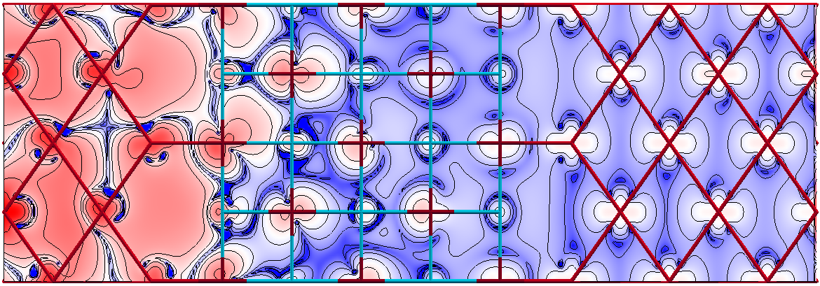
Fig. 11 presents the transmission in the MTJ’s P magnetic state for both spin channels, and in the AP magnetic state. Comparing with the ideal case (Fig. ), we find that both the P spin down and AP transmissions are practically unaffected by the defect. The spin up transmission is even more concentrated around the point than before. The TMR value reaches 1423%, which is as high as when the F/M center is positioned next to the interfacial layer.
 |
 |
 |
| (a) | (b) | (c) |
If we compare the spin up transmission in Fig. 11 and 8(c), we infer that the shape of the transmission reflects the symmetry/orientation of the M center. Indeed, when the M center is generated in a MgO plane parallel to the interfaces, the two oxygen vacancies lie along the diagonal, and a propagating electron simultaneously encounters both oxygen vacancies. This explains the elongation of the transmission peak along the diagonal of the plane in Fig. 8(c). On the other hand, when the M center is partially along the transport direction, i.e., in the plane, such that the two oxygen vacancies are in adjacent planes, the propagating electron reaches the first oxygen vacancy and then the second. As a result, the transmission is now along the direction in the BZ (Fig. 11). The transmission peaks are of same intensity because, owing to the symmetrical MgO spacer, electrons propagating from the left and the right electrodes see the same potential landscape.
This preservation of high TMR thanks to a P transmission channel that is concentrated at the point illustrates how the scenario of a M center, at the barrier’s center and partly directed along the tunnelling direction, can also concurrently generate high spintronic performance alongside a low barrier height.
V Conclusion
We have analyzed the electronic properties of single (F centers) and paired (M centers) oxygen vacancies in bulk MgO and in the MgO spacer of Fe/MgO/Fe MTJs, and their impact on ballistic spin- and symmetry-polarized transport. As detailed below, we conclude that the experimental sample preparation techniques associated with the concurrent observation of high TMR and low barrier heights can be theoretically explained in terms of the presence of oxygen vacancies in the barrier, especially near a MTJ interface.
The M center generates two doubly occupied energy levels within the MgO band gap that mimick the bonding (M1) and antibonding (M2) atomic-like states created due to two interacting F centers. As a result, the M center’s antibonding M2 state generates a lower tunnelling barrier height than does the F center. The energy level associated with a M2 center is shifted from -0.7 eV up to -0.2 eV below the Fermi level when we switch from an Fe to a Co interface, in agreement with the 0.5 eV change in work function of the Fe and Co surfaces. The M center’s energy levels remain unchanged upon moving the M center from the MTJ interface to the barrier middle, and upon changing its orientation relative to the interfaces. Our results therefore explicitly ascribe the experimental barrier heights of 0.4 eV to the presence of paired oxygen vacancies within the MgO barrier.
Incorporating either a F or M center within a Fe/MgO/Fe magnetic tunnel junction can decrease the transmission of the P spin up channel, while increasing somewhat that of the P spin down and AP channels. As a result the theoretical TMR can drop by up to two orders of magnitude, from 10000% to 100%. Overall, M centers tend to maintain a transmission maximum at the point for the P spin up channel, with only a small broadening, while F centers introduce scattering to higher -vectors, thereby decreasing the channel’s conductance. F and M centers induce only small increases in the P spin down and AP conductances. Consequently, the TMR is generally higher for transport across M centers than for F centers. Since the formation energy of a M center is lower than that of two F centers, annealing can induce the preferential presence of M centers over F centers, which in turn promotes higher spintronic performanceTaudul et al. (2017).
Our study indicates that the position of F and M centers crucially impacts magnetotransport. Compared to the case of an ideal junction, defects located on the interfacial MgO layer induce practically no change in either the shape of the transmission distribution or its amplitude. The resulting TMR reaches around 4000%, and the system amounts to an ideal MTJ with a barrier of reduced height and effective thickness. Moving the defect away from the interface reduces the P spin up transmission, and thus TMR, especially for the F center. This theoretical insight is compatible with the likely presence in experiments of oxygen vacancies at the lower MTJ interface when the MgO barrier is grown by oxidizing thin layers of metallic Mg deposited atop the lower ferromagnetic metallic electrode while avoiding the latter’s oxidationDahmani (2012); Dave et al. (2006). It is also in line with the role of interfacial oxygen vacancies in promoting perpendicular magnetic anisotropy in the adjacent ultrathin ferromagnetic filmsYang et al. (2011); Dieny and Chshiev (2017) of MgO-class MTJs with perpendicular magnetization. Finally, we find that orienting a M center at the barrier center so as to partly point along the transmission direction yields TMR 1000%.
Our study thus identifies conditions on the nature and positioning within the MgO of single/double oxygen vacancies so as to obtain predicted TMR values in excess of 1000% in MTJs with low barrier heights, in line with TMR amplitudes reported experimentallyIkeda et al. (2008). Our theoretical results thus reconcile the simultaneous presence of high TMR and low barrier heights in MgO-class MTJs by ascribing them to the presence of oxygen vacancies. Looking ahead, the respectively 3ML and 3-4ML effective physical size of the F and M centers condition not only the minimum barrier thickness for sizeable TMR (around 3MLSkowronski et al. (2010)), but also the MTJ’s lateral size. Technological progress has enabled the demonstration of working MTJs with a lateral size down to 4.3nmWatanabe et al. (2018). Experiments are thus approaching the 7-8ML (i.e 2nm) limit estimated for a M center to retain its electronic propertiesTaudul et al. (2017). Our work provides a much-needed theoretical basis to move beyond the mostly unsuspected, fortuitous defect engineering of spintronic performance that has thus far propelled MgO-based spintronics and its applications.
Acknowledgements.
This work was performed using HPC resources from the Strasbourg Mesocenter and from the GENCI-CINES Grant gem1100. MB acknowledges funding from the Agence Nationale de la Recherche (ANR-14-CE26-0009-01) and the Labex NIE "Symmix" project (ANR-11-LABX-0058 NIE) and thanks F. Schleicher, D. Lacour, M. Hehn, F. Montaigne, S. Boukari and W. Weber for useful discussions.- Žutić et al. (2004) I. Žutić, J. Fabian, and S. Das Sarma, Reviews of Modern Physics 76, 323 (2004), ISSN 0034-6861, eprint 0405528, URL https://link.aps.org/doi/10.1103/RevModPhys.76.323.
- Makarov et al. (2016) A. Makarov, T. Windbacher, V. Sverdlov, and S. Selberherr, Semiconductor Science and Technology 31, 113006 (2016), ISSN 0268-1242, URL http://stacks.iop.org/0268-1242/31/i=11/a=113006?key=crossref.9886421ee8fd6181b510e1a549c99b70.
- Lu et al. (2016) J. W. Lu, E. Chen, M. Kabir, M. R. Stan, and S. A. Wolf, International Materials Reviews 61, 456 (2016), ISSN 0950-6608, URL http://www.tandfonline.com/doi/full/10.1080/09506608.2016.1204097.
- Peng et al. (2014) S. Z. Peng, Y. G. Zhang, M. X. Wang, Y. G. Zhang, and W. Zhao, in Wiley Encyclopedia of Electrical and Electronics Engineering (John Wiley & Sons, Inc., Hoboken, NJ, USA, 2014), 12, pp. 1–16, ISBN 9780471346081, URL http://dx.doi.org/10.1002/047134608X.W8231{%}5Cnhttp://doi.wiley.com/10.1002/047134608X.W8231http://doi.wiley.com/10.1002/047134608X.W8231.
- Locatelli et al. (2013) N. Locatelli, V. Cros, and J. Grollier, Nature Materials 13, 11 (2013), ISSN 1476-1122, 1476-4660, URL http://www.nature.com/doifinder/10.1038/nmat3823.
- Moodera et al. (1995) J. S. Moodera, L. R. Kinder, T. M. Wong, and R. Meservey, Physical Review Letters 74, 3273 (1995), URL https://link.aps.org/doi/10.1103/PhysRevLett.74.3273.
- Wang et al. (2004) D. Wang, C. Nordman, J. M. Daughton, Z. Qian, and J. Fink, IEEE Transactions on Magnetics 40, 2269 (2004).
- MacLaren et al. (1999) J. M. MacLaren, X.-G. Zhang, W. H. Butler, and X. Wang, Physical Review B 59, 5470 (1999), URL https://link.aps.org/doi/10.1103/PhysRevB.59.5470.
- Butler et al. (2005) W. H. Butler, X. G. Zhang, S. Vutukuri, M. Chshiev, and T. C. Schulthess, IEEE Transactions on Magnetics 41, 2645 (2005).
- Butler (2008) W. H. Butler, Science and Technology of Advanced Materials 9, 014106 (2008), ISSN 1468-6996, URL http://www.tandfonline.com/doi/full/10.1088/1468-6996/9/1/014106.
- Zhang and Butler (2003) X.-G. Zhang and W. H. Butler, Journal of Physics: Condensed Matter 15, R1603 (2003).
- Butler et al. (2001a) W. H. Butler, X.-G. Zhang, T. C. Schulthess, and J. M. MacLaren, Physical Review B 63, 092402 (2001a), URL https://link.aps.org/doi/10.1103/PhysRevB.63.092402.
- Ikeda et al. (2008) S. Ikeda, J. Hayakawa, Y. Ashizawa, Y. M. Lee, K. Miura, H. Hasegawa, M. Tsunoda, F. Matsukura, and H. Ohno, Applied Physics Letters 93, 082508 (2008), ISSN 0003-6951, 1077-3118, URL http://scitation.aip.org/content/aip/journal/apl/93/8/10.1063/1.2976435.
- Kent and Worledge (2015) A. D. Kent and D. C. Worledge, Nature Nanotechnology 10, 187 (2015), ISSN 1748-3387, URL http://www.nature.com/nnano/journal/v10/n3/full/nnano.2015.24.html.
- Chappert et al. (2007) C. Chappert, A. Fert, and F. N. V. Dau, Nature Materials 6, 813 (2007).
- Ikeda et al. (2007) S. Ikeda, J. Hayakawa, Y. M. Lee, F. Matsukura, Y. Ohno, T. Hanyu, and H. Ohno, IEEE Transactions on Electron Devices 54, 991 (2007).
- Halisdemir et al. (2016) U. Halisdemir, F. Schleicher, D. J. Kim, B. Taudul, D. Lacour, W. S. Choi, M. Gallart, S. Boukari, G. Schmerber, V. Davesne, et al., in Society of Photo-Optical Instrumentation Engineers (SPIE) Conference Series (2016), vol. 9931, p. 99310H, URL http://proceedings.spiedigitallibrary.org/proceeding.aspx?doi=10.1117/12.2239017.
- Meyerheim et al. (2001) H. L. Meyerheim, R. Popescu, J. Kirschner, N. Jedrecy, M. Sauvage-Simkin, B. Heinrich, and R. Pinchaux, Physical Rreview Letters 87, 076102 (2001).
- Zhang et al. (2003) X.-G. Zhang, W. H. Butler, and A. Bandyopadhyay, Physical Review B 68, 092402 (2003), URL https://link.aps.org/doi/10.1103/PhysRevB.68.092402.
- Bonell et al. (2009) F. Bonell, S. Andrieu, A. M. Bataille, C. Tiusan, and G. Lengaigne, Physical Review B 79, 224405 (2009), ISSN 1098-0121, URL https://link.aps.org/doi/10.1103/PhysRevB.79.224405.
- Hayakawa et al. (2006) J. Hayakawa, S. Ikeda, Y. M. Lee, F. Matsukura, and H. Ohno, Applied Physics Letters 89, 232510 (2006), eprint https://doi.org/10.1063/1.2402904, URL https://doi.org/10.1063/1.2402904.
- Miyajima et al. (2009) T. Miyajima, T. Ibusuki, S. Umehara, M. Sato, S. Eguchi, M. Tsukada, and Y. Kataoka, Applied Physics Letters 94, 122501 (2009).
- Kozina et al. (2010) X. Kozina, S. Ouardi, B. Balke, G. Stryganyuk, G. H. Fecher, C. Felser, S. Ikeda, H. Ohno, and E. Ikenaga, Applied Physics Letters 96, 072105 (2010).
- Pinitsoontorn et al. (2008) S. Pinitsoontorn, A. Cerezo, A. K. Petford-Long, D. Mauri, L. Folks, and M. J. Carey, Applied Physics Letters 93, 071901 (2008).
- Rumaiz et al. (2011) A. K. Rumaiz, C. Jaye, J. C. Woicik, W. Wang, D. A. Fischer, J. Jordan-Sweet, and C. L. Chien, Applied Physics Letters 99, 222502 (2011).
- Kurt et al. (2010) H. Kurt, K. Rode, K. Oguz, M. Boese, C. C. Faulkner, and J. M. D. Coey, Applied Physics Letters 96, 262501 (2010).
- Mukherjee et al. (2015) S. Mukherjee, R. Knut, S. M. Mohseni, T. N. Anh Nguyen, S. Chung, Q. Tuan Le, J. Åkerman, J. Persson, A. Sahoo, A. Hazarika, et al., Physical Review B 91, 085311 (2015), URL https://link.aps.org/doi/10.1103/PhysRevB.91.085311.
- Wang et al. (2016) Z. Wang, M. Saito, K. P. McKenna, S. Fukami, H. Sato, S. Ikeda, H. Ohno, and Y. Ikuhara, Nano Letters 16, 1530 (2016).
- Bai et al. (2013) Z. Bai, L. Shen, Q. Wu, M. Zeng, J.-S. Wang, G. Han, and Y. P. Feng, Physical Review B 87, 014114 (2013), URL https://link.aps.org/doi/10.1103/PhysRevB.87.014114.
- Mizuguchi et al. (2007) M. Mizuguchi, Y. Suzuki, T. Nagahama, and S. Yuasa, Applied Physics Letters 91, 012507 (2007).
- Bean et al. (2017) J. J. Bean, M. Saito, S. Fukami, H. Sato, S. Ikeda, H. Ohno, Y. Ikuhara, and K. P. McKenna, Scientific Reports 7, 45594 (2017), ISSN 2045-2322, URL http://www.nature.com/articles/srep45594.
- Schleicher et al. (2014) F. Schleicher, U. Halisdemir, D. Lacour, M. Gallart, S. Boukari, G. Schmerber, V. Davesne, P. Panissod, D. Halley, H. Majjad, et al., Nature Communications 5, 4547 (2014).
- Rosenblatt et al. (1989) G. H. Rosenblatt, M. W. Rowe, G. P. Williams, R. T. Williams, and Y. Chen, Physical Review B 39, 10309 (1989), ISSN 0163-1829, URL https://link.aps.org/doi/10.1103/PhysRevB.39.10309.
- Gibson et al. (1994) A. Gibson, R. Haydo, and J. P. LaFemina, Physical Review B 50, 2582 (1994).
- Velev et al. (2007) J. P. Velev, K. D. Belashchenko, S. S. Jaswal, and E. Y. Tsymbal, Applied Physics Letters 90, 072502 (2007).
- Velve et al. (2007) J. P. Velve, M. Y. Zhuravlev, K. D. Belashchenko, S. S. Jaswal, E. Y. Tsymbal, T. Katayama, and S. Yuasa, IEEE Transactions on Magnetics 43, 2770 (2007).
- Kim et al. (2010) D. J. Kim, W. S. Choi, F. Schleicher, R. H. Shin, S. Boukari, V. Davesne, C. Kieber, J. Arabski, G. Schmerber, E. Beaurepaire, et al., Applied Physics Letters 97, 263502 (2010), ISSN 00036951, URL http://scitation.aip.org/content/aip/journal/apl/97/26/10.1063/1.3531652.
- Studniarek et al. (2017) M. Studniarek, U. Halisdemir, F. Schleicher, B. Taudul, E. Urbain, S. Boukari, M. Hervé, C.-H. Lambert, A. Hamadeh, S. Petit-Watelot, et al., Advanced Materials 29 (2017), ISSN 1521-4095, 1606578, URL http://dx.doi.org/10.1002/adma.201606578.
- Miao et al. (2008) G. Miao, Y. Park, J. Moodera, M. Seibt, G. Eilers, and M. Münzenberg, Physical Review Letters 100, 246803 (2008), ISSN 0031-9007, 1079-7114, URL http://link.aps.org/doi/10.1103/PhysRevLett.100.246803.
- Yuasa et al. (2004) S. Yuasa, T. Nagahama, A. Fukushima, Y. Suzuki, and K. Ando, Nature Materials 3, 868 (2004), URL http://www.nature.com/doifinder/10.1038/nmat1257.
- Parkin et al. (2004) S. S. P. Parkin, C. Kaiser, A. Panchula, P. M. Rice, B. Hughes, M. Samant, and S.-H. Yang, Nature Materials 3, 862 (2004).
- Mitani et al. (2003) S. Mitani, T. Moriyama, and K. Takanashi, Journal of Applied Physics 93, 8041 (2003).
- Lu et al. (2009) Y. Lu, M. Tran, H. Jaffrès, P. Seneor, C. Deranlot, F. Petroff, J. M. George, B. Lépine, S. Ababou, and G. Jézéquel, Physical Review Letters 102, 176801 (2009), ISSN 0031-9007, 1079-7114, URL http://link.aps.org/doi/10.1103/PhysRevLett.102.176801.
- Teixeira et al. (2011) J. M. Teixeira, J. Ventura, J. P. Araujo, J. B. Sousa, P. Wisniowski, S. Cardoso, and P. P. Freitas, Physical Review Letters 106, 196601 (2011).
- Ke et al. (2010) Y. Ke, K. Xia, and H. Guo, Physical Review Letters 105, 236801 (2010), URL https://link.aps.org/doi/10.1103/PhysRevLett.105.236801.
- McKenna and Blumberger (2012) K. P. McKenna and J. Blumberger, Physical Review B 86, 245110 (2012).
- Taudul et al. (2017) B. Taudul, E. N. Monteblanco, U. Halisdemir, D. Lacour, F. Schleicher, F. Montaigne, E. Beaurepaire, S. Boukari, M. Hehn, M. Alouani, et al., Advanced Electronic Materials 3 (2017), ISSN 2199-160X.
- Schleicher et al. (2018) F. Schleicher, B. Taudul, U. Halisdemir, K. Katcko, E. Monteblanco, D. Lacour, S. Boukari, F. Montaigne, E. Urbain, L. M. Kandpal, et al., arXiv:1711.05643v1 (2018).
- Smogunov et al. (2004) A. Smogunov, A. D. Corso, and E. Tosatti, Physical Review B 70, 045417 (2004).
- Kresse and Furthmüller (1996) G. Kresse and J. Furthmüller, Physical Review B 54, 11169 (1996).
- Kresse and Joubert (1999) G. Kresse and D. Joubert, Physical Review B 59, 1758 (1999).
- Blöchl (1994) P. E. Blöchl, Physical Review B 50, 17953 (1994).
- Perdew et al. (1996) J. P. Perdew, K. Burke, and M. Ernzerhof, Physical Review Letters 77, 3865 (1996), ISSN 0031-9007, eprint 0927-0256(96)00008, URL https://link.aps.org/doi/10.1103/PhysRevLett.77.3865.
- Paier et al. (2006) J. Paier, M. Marsman, K. Hummer, G. Kresse, I. C. Gerber, and J. G. Ángyán, The Journal of Chemical Physics 124, 154709 (2006).
- Butler et al. (2001b) W. H. Butler, X.-G. Zhang, T. C. Schulthess, and J. M. MacLaren, Physical Review B 63, 054416 (2001b).
- Urano and Kanaji (1988) T. Urano and T. Kanaji, Journal of the Physical Society of Japan (1988), ISSN 13474073.
- Wulfhekel et al. (2001) W. Wulfhekel, M. Klaua, D. Ullmann, F. Zavaliche, J. Kirschner, R. Urban, T. Monchesky, and B. Heinrich, Applied Physics Letters 78, 509 (2001).
- Hayakawa et al. (2005) J. Hayakawa, S. Ikeda, F. Matsukura, H. Takahashi, and H. Ohno, Japanese Journal of Applied Physics 44, L587 (2005), URL http://iopscience.iop.org/article/10.1143/JJAP.44.L587/meta.
- Landauer (1987) R. Landauer, Zeitschrift für Physik B Condensed Matter 68, 217 (1987).
- Büttiker et al. (1985) M. Büttiker, Y. Imry, R. Landauer, and S. Pinhas, Physical Review B 31, 6207 (1985), ISSN 0163-1829, URL https://link.aps.org/doi/10.1103/PhysRevB.31.6207.
- Giannozzi et al. (2009) P. Giannozzi, S. Baroni, N. Bonini, M. Calandra, R. Car, C. Cavazzoni, D. Ceresoli, G. L. Chiarotti, M. Cococcioni, I. Dabo, et al., Journal of Physics: Condensed Matter 21, 395502 (2009), URL http://www.quantum-espresso.org.
- Perdew and Wang (1992) J. P. Perdew and Y. Wang, Physical Review B 45, 13244 (1992), URL https://link.aps.org/doi/10.1103/PhysRevB.45.13244.
- Velev et al. (2005) J. P. Velev, K. D. Belashchenko, D. A. Stewart, M. van Schilfgaarde, S. S. Jaswal, and E. Y. Tsymbal, Physical Review Letters 95, 216601 (2005), URL https://link.aps.org/doi/10.1103/PhysRevLett.95.216601.
- Bowen et al. (2006) M. Bowen, A. Barthélémy, V. Bellini, M. Bibes, P. Seneor, E. Jacquet, J. P. Contour, and P. Dederichs, Physical Review B 73, 140408 (2006).
- Taudul (2017) B. Taudul, Ph.D. thesis, Université de Strasbourg, Institut de Physique et Chimie des Matériaux de Strasbourg (2017), URL http://www.theses.fr/2017STRAE042/document.
- Mathon and Umerski (2001) J. Mathon and A. Umerski, Physical Review B 63, 220403(R) (2001).
- Dahmani (2012) F. Dahmani, Japanese Journal of Applied Physics 73, 043002 (2012).
- Dave et al. (2006) R. W. Dave, G. Steiner, J. M. Slaughter, J. J. Sun, B. Craigo, S. Pietambaram, K. Smith, G. Grynkewich, M. DeHerrera, J. Åkerman, et al., IEEE Transactions on Magnetics 42, 1935 (2006).
- Yang et al. (2011) H. X. Yang, M. Chshiev, B. Dieny, J. H. Lee, A. Manchon, and K. H. Shin, Physical Review B 84, 054401 (2011), URL https://link.aps.org/doi/10.1103/PhysRevB.84.054401.
- Dieny and Chshiev (2017) B. Dieny and M. Chshiev, Reviews of Modern Physics 89, 025008 (2017), URL https://link.aps.org/doi/10.1103/RevModPhys.89.025008.
- Skowronski et al. (2010) W. Skowronski, T. Stobiecki, J. Wrona, K. Rott, A. Thomas, G. Reiss, and S. van Dijken, Journal of Applied Physics 107, 093917 (2010), ISSN 0021-8979, 1089-7550, URL http://scitation.aip.org/content/aip/journal/jap/107/9/10.1063/1.3387992.
- Watanabe et al. (2018) K. Watanabe, B. Jinnai, S. Fukami, H. Sato, and H. Ohno, Nature Communications 9, 663 (2018), ISSN 2041-1723, eprint 1712.08774, URL http://dx.doi.org/10.1038/s41467-018-03003-7http://www.nature.com/articles/s41467-018-03003-7.