Electronic transmission in the lateral heterostructure of semiconducting and metallic transition-metal dichalcogenide monolayers
Abstract
We investigate the electronic transport property of lateral heterojunctions of semiconducting and metallic transition-metal dichalcogenide monolayers, MoSe2 and NbSe2, respectively. We calculate the electronic transmission probability by using a multi-orbital tight-binding model based on the first-principles band structure. The transmission probability depends on the spin and valley degrees of freedom. This dependence qualitatively changes by the interface structure. The heterostructure with a zig-zag interface preserves the spin and the valley of electron in the transmission process. On the other hand, the armchair interface enables conduction electrons to transmit with changing the valley and increases the conductance in hole-doped junctions due to the valley-flip transmission. We also discuss the spin and valley polarizations of electronic current in the heterojunctions.
I Introduction
Transition-metal dichalcogenides (TMDCs) are layered materials of atomically thin two-dimensional crystal consisting of transition-metal and chalcogen atoms, and the monolayer has been attracted much attention in condensed matter physics. In semiconducting TMDC monolayers, electrons have two discrete degrees of freedom, spin and valley, due to the band structure.Xiao et al. (2012); Zibouche et al. (2014) Strong spin-orbit coupling (SOC) leads to spin-related physics in TMDCs,Shan et al. (2013); Klinovaja and Loss (2013) and the valley-dependent Berry curvature causes valley Hall effect.Mak et al. (2012) Therefore, TMDC monolayers have been researched for applications in spintronicsSuzuki et al. (2014); Yuan et al. (2014); Habe and Koshino (2015); Shao et al. (2016) and valleytronicsCao et al. (2012); Zeng et al. (2012); Gong et al. (2013); Ye et al. (2016). Since the electronic spin direction is locked to the valley due to the strong SOC, the valleytronics and the spintronics can be combined, e.g., the valley can be detected as the spin.
Stable monolayers can be fabricated by cleaving from a crystalHelveg et al. (2000); Mak et al. (2010); Coleman et al. (2011) or chemical vapor deposition (CVD) on a substrateLee et al. (2012); Dong and Kuljanishvili (2017). The experimental techniques enable to compose heterostructures consisting of different atomic layers. The first-designed heterostructure is a stacking of different atomic layers, so-called van der Waals heterostructure, and it has opened several areas of research and application: opticsHe et al. (2014), electric transportJi et al. (2017), and exciton physicsBaranowski et al. (2017); Xu et al. (2018). The lateral heterostructure is composed of two atomic layers bonded as a single layer, and that of semiconducting TMDCs has been realized by CVD.Huang et al. (2014); Gong et al. (2014); Duan et al. (2014); Chen et al. (2015a, b); Zhang et al. (2015); He et al. (2016) The semiconducting heterojunction has been investigated theoreticallyKang et al. (2013); Habe and Koshino (2015) and experimentally applied to p-n junctionLi et al. (2015); Najmzadeh et al. (2016), valleytronicsUllah et al. (2017), and optoelectronicsSon et al. (2016). Such the junction provides novel electronic properties for semiconducting TMDCs.
Metallic TMDCs have also attracted much attention in terms of condensed phases. The TMDC of group-V transition metal atom, Nb and Ta, is metallic and has been discovered to show superconductivityLu et al. (2015); Wang et al. (2017) and the charge density wave (CDW)Ugeda et al. (2015); Xi et al. (2015), even in the monolayer. NbSe2 monolayer, even in the normal phase, has qualitatively different property of conduction electrons from the semiconducting monolayers. There are three Fermi pockets in the first Brillouin zone whereas the semiconducting members have two pockets called the and valleys. Each pocket has both the up-spin and down-spin states. Thus, the correlation between the spin and valley degrees of freedom, the key property of semicondcuting monolayers for combining the spintronics and the valleytronics , is absent in the metallic monolayers. We consider the lateral heterojunction of the metallic and semiconducting TMDC monolayers and show that it induces the correlation between the spin and the three valleys.
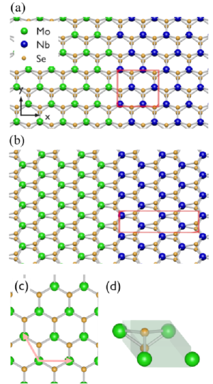
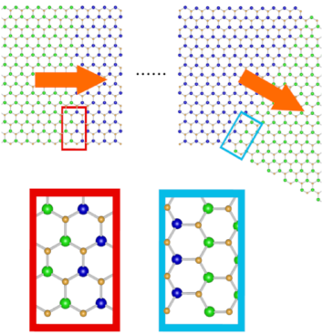
In this paper, we report our investigation of the spin and valley-dependent electronic transport property of the lateral heterojunction of MoSe2 and NbSe2 monolayers, metallic and semiconducting TMDCs, respectively. We consider two types of interface for such the junction as shown in Fig. 1. The electronic transmission is qualitatively different in two types of interface, the armchair interface in (a) and zig-zag interface in (b). We compute the spin and valley-dependence of electronic conductance by using first-principles band calculation and lattice Green’s function method, and we show the valley-spin correlated transmission effect. This result gives a fundamental knowledge for spintronics and valleytronics in lateral heterojunctions.
II Band structure
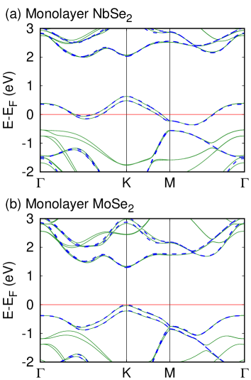
The TMDC monolayer consists of three sublayers, a sublayer of transition-metal atoms sandwiched by two sublayers of chalcogen atoms. The transition-metal atoms, Nb or Mo, and chalcogen atoms, Se, are strongly bonded and form two-dimensional hexagonal lattice as shown in Fig. 1 (c). We plot the band structure of pristine monolayer of NbSe2 and MoSe2 in Figs. 2 (a) and (b), respectively.
These bands are calculated by using quantum-ESPRESSO, a first-principles calculation codeGiannozzi et al. (2009). Here, we adopt a projector augmented wave (PAW) method with a generalized gradient approximation (GGA) functional including SOC, the cut-off energy of plane wave basis 50 Ry, and the conversion criterion 10-8 Ry. The lattice parameters are also calculated by lattice-relaxation code of quantum-ESPRESSO as Å and Å in NbSe2, and Å and Å in MoSe2, where () is the horizontal (vertical) distance between nearest neighbor transition-metal (chalcogen) atoms.
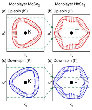
MoSe2 monolayer is a semiconductor and has a direct gap at the and points in the Brillouin zone. At the band edge, the electronic states split into two spin states due to SOC (see Fig. 2), where the spin-split in the valence band is much larger than that in the conduction band. Here, the spin axis is restricted in the out-of-plane direction due to crystal symmetry.Xiao et al. (2012) We show the Fermi surface of electron-doped and hole-doped monolayers with the charge density cm-2 and cm-2, respectively, in Fig. 3. The Fermi pockets appear around the and points, and each pocket is so-called a valley.

In the hole-doped monolayer, the spin is fully polarized in each valley up to cm-2, the experimentally feasible charge density by using electrostatic gating.Zhang et al. (2012) The spin polarization direction is opposite in two valleys due to time-reversal symmetry, and total spin-polarization is absent. Under the condition of , on the other hand, both the spin states are present in each valley. The electrons in MoSe2 can be characterized by spin and valley indexes at any charge density.
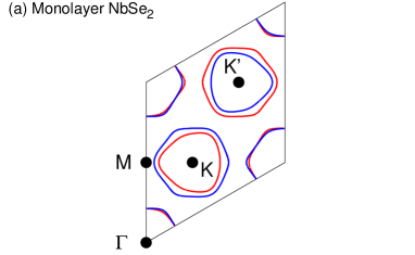
In NbSe2 monolayer, the band is quite similar to that of MoSe2 due to the crystal structure as shown in Fig. 2, but the band is partially filled even at the charge neutral point because the atomic number of Nb is one less than Mo. We show the Fermi surface of pristine NbSe2 monolayer in Fig. 4. The Fermi pockets appear around three high-symmetry points, the , , and points. We represent the pockets as the , , and valleys in what follows. In every valleys, both the two spin states are present. The spin polarization is non-zero and opposite each other in the and valleys, but the populations of two spins are equal to each other in the valley. Every Fermi pockets are strongly trigonal warping due to three-fold symmetry of crystal structure.
III Calculation method
To calculate the electronic transmission probability, we adopt a tight-binding model in bases of Wannier functions, where the hopping integrals are computed from the first-principles band structure in Sec. II. The maximally localized Wanner functions and spin-dependent hopping integrals are computed by using Wannier90Mostofi et al. (2008). Here, we adopt three -orbitals , , and of transition-metal atom , and three superpositions of -orbitals of top selenium Set and bottom one Seb as , , and with . These orbitals have even parity under mirror operation in the axis and they are independent of odd parity orbitals in the electronic structure. We show the band structure calculated by the tight-binding model in Fig. 2. It well reproduces the first-principles bands.
We simulate the electronic transmission in lateral heterostructures at zero temperature by using the multi-orbital tight-binding model including the interface between MoSe2 and NbSe2 monolayers. Here, NbSe2 monolayer shows the phase transition, CDW and superconductivity, at low temperature but we consider normal states of NbSe2 for investigating the fundamental transport property of metallic NbSe2 monolayer. We assume a commensurate interface, where two atomic layers are bonded without dangling and misalignment as shown in Fig. 1, and a periodic boundary condition parallel to the interface. The incident electronic wave with in MoSe2 transmits to NbSe2 as a wave with , and thus the transmission coefficient is defined at each . In what follows, we represent both the wave numbers, and , by . Despite the mismatch of lattice parameters, such a commensurate heterostructure has been fabricated experimentally.Li et al. (2015); Gong et al. (2014) To use lattice Green’s function method, we consider a unit cell including four transition-metal atoms and eight Se as shown in Fig. 1. Here, we adopt the hopping matrix in NbSe2 as that between MoSe2 and NbSe2 because the outer shell of Mo and Nb atoms is same as 4-orbitals, and the hopping integral is similar to each other in the two monolayers.
We calculate the transmission probability by using lattice Green’s function method for multi-orbital tight-binding modelAndo (1991); Habe and Koshino (2015, 2016), where and represent the incoming and outgoing waves in MoSe2 and NbSe2, respectively. The conductance per unit width is given by
| (1) |
Here, and are the velocity along the axis for the outgoing wave in NbSe2 and the incoming wave in MoSe2, respecitvely. We define the positive direction in the axis as the transmission direction. Thus, the electronic waves and have the positive velocity in the axis. The wave function is represented by the periodic part , wave amplitudes of Wanner functions, in a unit cell and the phase shift in the transmission process between adjacent cells. The coefficients are the eigenfunction and eigenvalue of the following equation for each in pristine MoSe2 and NbSe2 monolayers as
| (2) |
with the onsite potential , and the right-going and left-going hopping matrix and , respectively. The velocity in the axis is calculated by with the velocity operator as
| (3) |
where is the length of square unit cell in Fig. 1 along . Here, the Fermi energy is computed under the condition of a charge density as
| (4) |
where is the charge density of nuclei, and is the energy dispersion in Fig. 2. We consider the charge induction by using a top or back gate being homogeneous in the plane. By gating, opposite charges are induced in the substrate and homogeneously distributed in the plane. Thus, we can assume that the induced charges in the heterojunction are distributed homogeneously, i.e., , in the plane due to the local charge neutrality. Then, the Fermi energy is also applied to the MoSe2 and NbSe2 regions in the lateral heterojunction. We also calculate of incoming and outgoing waves by using , and thus we can characterize these waves by the valley degree of freedom by referring to the Fermi surface in Figs. 3 and 4. Therefore, the wave index, and , is given by the valley index and the spin index . By picking up a spin and a valley, it is possible to calculate the conductance of spin-polarized electrons transferring between two valleys.
IV Numerical results
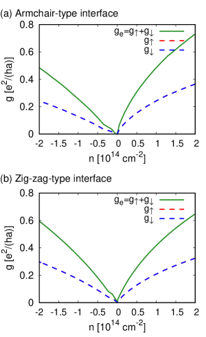
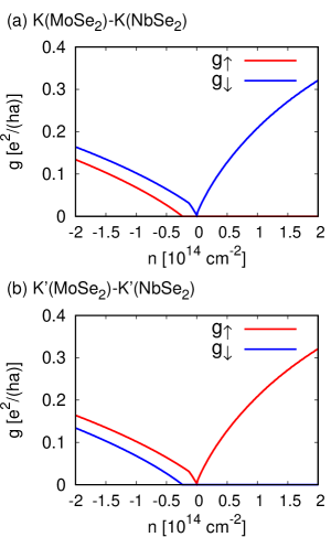
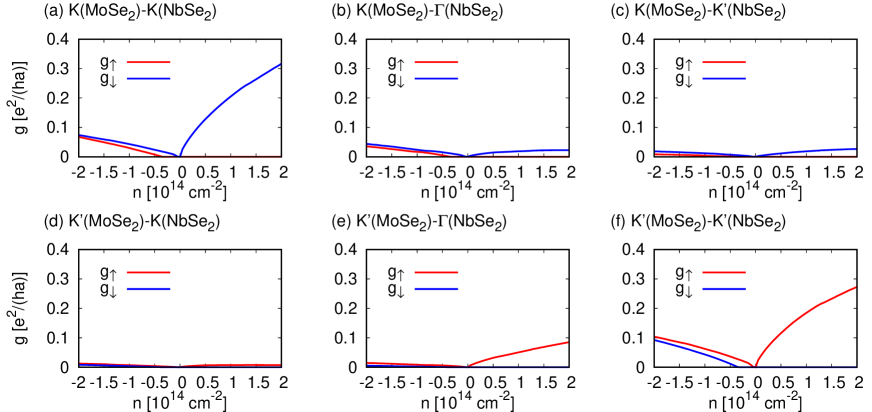
First, we show the charge density-dependence of electric conductance in Fig. 5. The conductance drops around in both the two types of heterostructures with an armchair-type interface and a zig-zag-type interface in Fig. 1 (a) and (b), respectively, and it monotonically increases with . This is because the Fermi level is in the insulating gap under , and the conducting channels increase with in MoSe2. At every non-zero charge densities, the heterostructure with the armchair-type interface gives a larger than that with the zig-zag-type interface. The armchair interface allows electrons transferring between different valleys, e.g., and , in MoSe2 and NbSe2 as discussed below, and thus it enhances the total transmission probability. In the transmission process, the electronic spin is conserved due to the mirror symmetry in the axis, the out-of-plane direction. Thus, the conductance is separated into that of up-spin electrons and down-spin electrons . In TMDC monolayers, the spin relaxation is suppressed even in the presence of non-magnetic impurity due to the mirror symmetry.Ochoa and Roldán (2013); Ochoa et al. (2013); Habe and Koshino (2016) The two spin components are balanced due to the equal population of two spins in the presence of time-reversal symmetry.
Nest, we show the valley-dependent conductance in the two types of heterostructures in Figs. 6 and 7. The heterostructure with a zig-zag interface preserves mirror symmetry in the axis. Thus, the transmission probability is equivalent in both the valleys as shown in Fig. 6. When passing through the zig-zag interface, electrons preserve the valley degree of freedom due to conservation of wave number parallel to the interface. Here, is parallel to the direction in Figs. 3 and 4, and the transmission of electron with is non-zero as long as electronic states are present in the Fermi surface of both MoSe2 and NbSe2. Since the spin is fully polarized in the and valleys on the condition of in MoSe2, the spin and valley are locked to each other in the transmission process. In , on the other hand, the up-spin and down-spin electrons flow above cm-2 in both the two valleys.
In Fig. 7, we show the spin and valley dependence of conductance of the heterojunction with an armchair-type interface. Valley-conserving transmission probability is similar to that in the zig-zag interface. Moreover, electrons in MoSe2 are able to transmit with switching the valley to as shown in (b) and (e), but the valley-switch between the and valleys is highly suppressed even in this heterostructure as shown in (c) and (d). The electronic flow in the valley carries the spin current in .
The spin flow is attributed to the difference of transmission coefficient for incoming electronic waves in the and valleys of MoSe2. Here, the transmission coefficient is defined as , which is the integrand in Eq. (1), and it depends on the ratio of Fermi velocity in the pristine NbSe2 and MoSe2. We show the Fermi velocity in MoSe2 and NbSe2 in Fig. 8, where the electronic states having the right-going velocity and being inside of dashed lines are corresponding to the wave vector holding conducting channels. The Fermi velocity of right-going states with down-spin is much smaller than that with up-spin in NbSe2. The spin current in the valley is caused by this anisotropy of Fermi velocity. The armchair interface allows us to obtain not only the spin-polarized electronic current in the valleys but also the valley polarized current between the and valleys, which can be observed by valley Hall effect due to the opposite Berry curvature in the two valleys.Xiao et al. (2012); Shan et al. (2013); Habe and Koshino (2017)
V Discussion
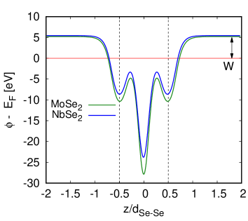
In the previous section, we consider the heterojunction with a charge density induced by electrostatic gating. In this section, we discuss the effect of chemical doping in the lateral heterojunction. The dopants form impurity levels inside the gap of semiconductor and pin the Fermi energy at a level without gating. Around the interface, the charge density is modulated due to the difference of work function between MoSe2 and NbSe2. We calculate the electrostatic potential for electrons as a function of , the out-of-plane coordinate, by using quantum-ESPRESSO and plot it referring to the Fermi level in Fig. 9. Here, we set the origin of at the transition-metal atoms and adopt the potential at as the vacuum level. The work function is defined by the vacuum level with respect to the Fermi energy. We compute the work function eV and eV, where is similar to a previous workLanzillo et al. (2015), and obtain the difference eV. Since the semiconducting TMDC, MoSe2, has a smaller work function than the metallic TMDC, NbSe2, a Schottky barrier is formed in the junction of electron-doped MoSe2 due to the modulation of doped carrier density. In the hole-doped heterostructure, on the other hand, the junction has a Ohmic contact.
Around the interface of realistic materials, charges transfer between two TMDCs due to the difference of work functions. The charge transfer modifies the Fermi energy near the interface and it can be treated as a contact resistance. It reduces the transmission probability but the spin and valley polarization is unchanged qualitatively because time-reversal and mirror symmetries are preserved. Furthermore, the control of contact resistance for atomic layered materials has been developing, e.g., graphene-metal junctionGiubileo and Bartolomeo (2017). In our calculation, we assume the uniform Fermi energy over each TMDC for analyzing an ideal transmission case.
Finally, we discuss the experimental observation associated with the spin and valley dependent transmission in the lateral heterojunction. We show that the spin of conduction electrons is not polarized at a single heterojunction as shown in Fig. 5. By combining the armchair and zig-zag interfaces, on the other hand, the two-interface heterojunction induces the spin and valley polarized current. In Fig. 10, the left interface changes the transmission probability between the and , and the right interface allows the equal transmission for the two valleys. Then, the spin and valley polarization induced by the left interface remains in the right MoSe2 region. Therefore, the spin and valley dependent transmission can be shown in the two-interface hererojunction experimentally.
VI Conclusion
We have investigated the electronic transport property of lateral heterojunctions of metallic NbSe2 monolayer and semiconducting MoSe2 monolayer and shown that the spin and valley dependence of conductance changes with the interface structure. The zig-zag interface conserves the spin and valley of conduction electron in the and valleys, and the conductance is independent of the valley and spin. This means that NbSe2 can be applied to the lead in spintronic or valleytronic devices of semiconducting TMDCs. When electrons pass through an armchair interface, the electronic spin is also conserved, but the valley, on the other hand, changes in the transmission process. This valley-flip increases the total transmission probability, and thus the conductance is larger than that with the zig-zag interface in . Moreover, the transmission probability is strongly depending on the spin and valley, and thus conduction electrons are spin-polarized in each valley. The lateral heterostructure can be useful in spintronics and valleytronics, and its transport properties studied here provide the opportunity to develop devices made by only atomic layers.
References
- Xiao et al. (2012) D. Xiao, G.-B. Liu, W. Feng, X. Xu, and W. Yao, Phys. Rev. Lett. 108, 196802 (2012).
- Zibouche et al. (2014) N. Zibouche, A. Kuc, J. Musfeldt, and T. Heine, Annalen der Physik 526, 395 (2014).
- Shan et al. (2013) W.-Y. Shan, H.-Z. Lu, and D. Xiao, Phys. Rev. B 88, 125301 (2013).
- Klinovaja and Loss (2013) J. Klinovaja and D. Loss, Phys. Rev. B 88, 075404 (2013).
- Mak et al. (2012) K. F. Mak, K. He, J. Shan, and T. F. Heinz, Nat Nano 7, 494 (2012).
- Suzuki et al. (2014) R. Suzuki, M. Sakano, Y. J. Zhang, R. Akashi, D. Morikawa, A. Harasawa, K. Yaji, K. Kuroda, K. Miyamoto, T. Okuda, K. Ishizaka, R. Arita, and Y. Iwasa, Nat. Nano. 9, 611 (2014).
- Yuan et al. (2014) H. Yuan, X. Wang, B. Lian, H. Zhang, X. Fang, B. Shen, G. Xu, Y. Xu, S.-C. Zhang, H. Y. Hwang, and Y. Cui, Nat. Nano. 9, 851 (2014).
- Habe and Koshino (2015) T. Habe and M. Koshino, Phys. Rev. B 91, 201407 (2015).
- Shao et al. (2016) Q. Shao, G. Yu, Y.-W. Lan, Y. Shi, M.-Y. Li, C. Zheng, X. Zhu, L.-J. Li, P. K. Amiri, and K. L. Wang, Nano Letters 16, 7514 (2016).
- Cao et al. (2012) T. Cao, G. Wang, W. Han, H. Ye, C. Zhu, J. Shi, Q. Niu, P. Tan, E. Wang, B. Liu, and J. Feng, Nature Commun. 3, 887 (2012).
- Zeng et al. (2012) H. Zeng, J. Dai, W. Yao, D. Xiao, and X. Cui, Nat. Nano. 7, 490 (2012).
- Gong et al. (2013) Z. Gong, G.-B. Liu, H. Yu, D. Xiao, X. Cui, X. Xu, and W. Yao, Nat. Commun. 4, 2053 (2013).
- Ye et al. (2016) Y. Ye, J. Xiao, H. Wang, Z. Ye, H. Zhu, M. Zhao, Y. Wang, J. Zhao, X. Yin, and X. Zhang, Nature Nanotechnology 11, 598 (2016).
- Helveg et al. (2000) S. Helveg, J. V. Lauritsen, E. Lægsgaard, I. Stensgaard, J. K. Nørskov, B. S. Clausen, H. Topsøe, and F. Besenbacher, Phys. Rev. Lett. 84, 951 (2000).
- Mak et al. (2010) K. F. Mak, C. Lee, J. Hone, J. Shan, and T. F. Heinz, Phys. Rev. Lett. 105, 136805 (2010).
- Coleman et al. (2011) J. N. Coleman, M. Lotya, A. O’Neill, S. D. Bergin, P. J. King, U. Khan, K. Young, A. Gaucher, S. De, R. J. Smith, I. V. Shvets, S. K. Arora, G. Stanton, H.-Y. Kim, K. Lee, G. T. Kim, G. S. Duesberg, T. Hallam, J. J. Boland, J. J. Wang, J. F. Donegan, J. C. Grunlan, G. Moriarty, A. Shmeliov, R. J. Nicholls, J. M. Perkins, E. M. Grieveson, K. Theuwissen, D. W. McComb, P. D. Nellist, and V. Nicolosi, Science 331, 568 (2011).
- Lee et al. (2012) Y.-H. Lee, X.-Q. Zhang, W. Zhang, M.-T. Chang, C.-T. Lin, K.-D. Chang, Y.-C. Yu, J. T.-W. Wang, C.-S. Chang, L.-J. Li, and T.-W. Lin, Adv. Mater. 24, 2320 (2012).
- Dong and Kuljanishvili (2017) R. Dong and I. Kuljanishvili, Journal of Vacuum Science & Technology B 35, 030803 (2017).
- He et al. (2014) J. He, K. Hummer, and C. Franchini, Phys. Rev. B 89, 075409 (2014).
- Ji et al. (2017) Z. Ji, H. Hong, J. Zhang, Q. Zhang, W. Huang, T. Cao, R. Qiao, C. Liu, J. Liang, C. Jin, L. Jiao, K. Shi, S. Meng, and K. Liu, ACS Nano 11, 12020 (2017).
- Baranowski et al. (2017) M. Baranowski, A. Surrente, L. Klopotowski, J. M. Urban, N. Zhang, D. K. Maude, K. Wiwatowski, S. Mackowski, Y. C. Kung, D. Dumcenco, A. Kis, and P. Plochocka, Nano Letters 17, 6360 (2017).
- Xu et al. (2018) W. Xu, D. Kozawa, Y. Liu, Y. Sheng, K. Wei, V. B. Koman, S. Wang, X. Wang, T. Jiang, M. S. Strano, and J. H. Warner, Small 14, 1703727 (2018).
- Huang et al. (2014) C. Huang, S. Wu, A. M. Sanchez, J. J. P. Peters, R. Beanland, J. S. Ross, P. Rivera, W. Yao, D. H. Cobden, and X. Xu, Nature Materials 13, 1096 (2014).
- Gong et al. (2014) Y. Gong, J. Lin, X. Wang, G. Shi, S. Lei, Z. Lin, X. Zou, G. Ye, R. Vajtai, B. I. Yakobson, H. Terrones, M. Terrones, B. Tay, J. Lou, S. T. Pantelides, Z. Liu, W. Zhou, and P. M. Ajayan, Nature Materials 13, 1135 (2014).
- Duan et al. (2014) X. Duan, C. Wang, J. C. Shaw, R. Cheng, Y. Chen, H. Li, X. Wu, Y. Tang, Q. Zhang, A. Pan, J. Jiang, R. Yu, Y. Huang, and X. Duan, Nature Nanotechnology 9, 1024 (2014).
- Chen et al. (2015a) K. Chen, X. Wan, W. Xie, J. Wen, Z. Kang, X. Zeng, H. Chen, and J. Xu, Advanced Materials 27, 6431 (2015a).
- Chen et al. (2015b) K. Chen, X. Wan, J. Wen, W. Xie, Z. Kang, X. Zeng, H. Chen, and J.-B. Xu, ACS Nano 9, 9868 (2015b).
- Zhang et al. (2015) X.-Q. Zhang, C.-H. Lin, Y.-W. Tseng, K.-H. Huang, and Y.-H. Lee, Nano Letters 15, 410 (2015).
- He et al. (2016) Y. He, A. Sobhani, S. Lei, Z. Zhang, Y. Gong, Z. Jin, W. Zhou, Y. Yang, Y. Zhang, X. Wang, B. Yakobson, R. Vajtai, N. J. Halas, B. Li, E. Xie, and P. Ajayan, Advanced Materials 28, 5126 (2016).
- Kang et al. (2013) J. Kang, S. Tongay, J. Zhou, J. Li, and J. Wu, Applied Physics Letters 102, 012111 (2013).
- Li et al. (2015) M.-Y. Li, Y. Shi, C.-C. Cheng, L.-S. Lu, Y.-C. Lin, H.-L. Tang, M.-L. Tsai, C.-W. Chu, K.-H. Wei, J.-H. He, W.-H. Chang, K. Suenaga, and L.-J. Li, Science 349, 524 (2015).
- Najmzadeh et al. (2016) M. Najmzadeh, C. Ko, K. Wu, S. Tongay, and J. Wu, Applied Physics Express 9, 055201 (2016).
- Ullah et al. (2017) F. Ullah, Y. Sim, C. T. Le, M.-J. Seong, J. I. Jang, S. H. Rhim, B. C. Tran Khac, K.-H. Chung, K. Park, Y. Lee, K. Kim, H. Y. Jeong, and Y. S. Kim, ACS Nano 11, 8822 (2017).
- Son et al. (2016) Y. Son, M.-Y. Li, C.-C. Cheng, K.-H. Wei, P. Liu, Q. H. Wang, L.-J. Li, and M. S. Strano, Nano Letters 16, 3571 (2016).
- Lu et al. (2015) J. M. Lu, O. Zheliuk, I. Leermakers, N. F. Q. Yuan, U. Zeitler, K. T. Law, and J. T. Ye, Science 350, 1353 (2015).
- Wang et al. (2017) H. Wang, X. Huang, J. Lin, J. Cui, Y. Chen, C. Zhu, F. Liu, Q. Zeng, J. Zhou, P. Yu, X. Wang, H. He, S. H. Tsang, W. Gao, K. Suenaga, F. Ma, C. Yang, L. Lu, T. Yu, E. H. T. Teo, G. Liu, and Z. Liu, Nature Communications 8, 394 (2017).
- Ugeda et al. (2015) M. M. Ugeda, A. J. Bradley, Y. Zhang, S. Onishi, Y. Chen, W. Ruan, C. Ojeda-Aristizabal, H. Ryu, M. T. Edmonds, H.-Z. Tsai, A. Riss, S.-K. Mo, D. Lee, A. Zettl, Z. Hussain, Z.-X. Shen, and M. F. Crommie, Nature Physics 12, 92 (2015).
- Xi et al. (2015) X. Xi, L. Zhao, Z. Wang, H. Berger, L. Forró, J. Shan, and K. F. Mak, Nature Nanotechnology 10, 765 (2015).
- Giannozzi et al. (2009) P. Giannozzi, S. Baroni, N. Bonini, M. Calandra, R. Car, C. Cavazzoni, D. Ceresoli, G. L. Chiarotti, M. Cococcioni, I. Dabo, A. Dal Corso, S. de Gironcoli, S. Fabris, G. Fratesi, R. Gebauer, U. Gerstmann, C. Gougoussis, A. Kokalj, M. Lazzeri, L. Martin-Samos, N. Marzari, F. Mauri, R. Mazzarello, S. Paolini, A. Pasquarello, L. Paulatto, C. Sbraccia, S. Scandolo, G. Sclauzero, A. P. Seitsonen, A. Smogunov, P. Umari, and R. M. Wentzcovitch, J. Phys.: Condens. Matter 21, 395502 (2009).
- Shi et al. (2013) H. Shi, H. Pan, Y.-W. Zhang, and B. I. Yakobson, Phys. Rev. B 87, 155304 (2013).
- Zhang et al. (2012) Y. Zhang, J. Ye, Y. Matsuhashi, and Y. Iwasa, Nano Letters 12, 1136 (2012).
- Mostofi et al. (2008) A. A. Mostofi, J. R. Yates, Y.-S. Lee, I. Souza, D. Vanderbilt, and N. Marzari, Computer Physics Communications 178, 685 (2008).
- Ando (1991) T. Ando, Phys. Rev. B 44, 8017 (1991).
- Habe and Koshino (2016) T. Habe and M. Koshino, Phys. Rev. B 93, 075415 (2016).
- Ochoa and Roldán (2013) H. Ochoa and R. Roldán, Phys. Rev. B 87, 245421 (2013).
- Ochoa et al. (2013) H. Ochoa, F. Guinea, and V. I. Fal’ko, Phys. Rev. B 88, 195417 (2013).
- Habe and Koshino (2017) T. Habe and M. Koshino, Phys. Rev. B 96, 085411 (2017).
- Lanzillo et al. (2015) N. A. Lanzillo, A. J. Simbeck, and S. K. Nayak, Journal of Physics: Condensed Matter 27, 175501 (2015).
- Giubileo and Bartolomeo (2017) F. Giubileo and A. D. Bartolomeo, Progress in Surface Science 92, 143 (2017).