figurec
Atomic-level Characterisation of Quantum Computer Arrays by Machine Learning
Atomic level qubits in silicon are attractive candidates for large-scale quantum computing, however, their quantum properties and controllability are sensitive to details such as the number of donor atoms comprising a qubit and their precise location. This work combines machine learning techniques with million-atom simulations of scanning-tunnelling-microscope (STM) images of dopants to formulate a theoretical framework capable of determining the number of dopants at a particular qubit location and their positions with exact lattice-site precision. A convolutional neural network was trained on 100,000 simulated STM images, acquiring a characterisation fidelity (number and absolute donor positions) of above 98% over a set of 17,600 test images including planar and blurring noise. The method established here will enable a high-precision post-fabrication characterisation of dopant qubits in silicon, with high-throughput potentially alleviating the requirements on the level of resource required for quantum-based characterisation, which may be otherwise a challenge in the context of large qubit arrays for universal quantum computing.
Of the leading platforms for the implementation of quantum computing architectures, qubits based on the spin of individual dopant atoms in silicon Kane_Nature_1998 ; Loss_PRA_1998 ; Zwanenburg_RMP_2013 ; Fuechsle_NN_2012 ; Salfi_PRX_2018 ; Pla_Nature_2012 ; Morello_Nature_2010 are growing in interest given the nexus with nanoelectronics engineering and the long coherence times Tyryshkin_Nat_Mat_2012 ; Saeedi_Science_2013 . For the exchange-based quantum computer design proposals Kane_Nature_1998 ; Loss_PRA_1998 ; Pica_PRB_2016 where the physical separations between atomic qubits are small (10-15 nm), the pathway for scale-up to large two-dimensional arrays generally relies on uniformity of control of qubits and their interactions. Even small variations at the level of one lattice-site for qubits based on single or multiple dopant atoms can significantly affect the design and control of logical operations. While the details of few qubit systems can be determined using electrostatics and electron spin resonance Wang_NatureSR_2016 and variations in interactrions mitigated by designing appropriate pulse schemes Testlin_PRA_2007 ; Hill_PRL_2007 , for large-scale arrays a reliable and fast method of identification (atom count per qubit) and characterisation (exact spatial location of atoms in lattice) is critical.
Machine intelligence techniques have been extremely productive in a wide range of applications including material design, medical imaging, and data science, where the design space is enormously large Butler_Nature_2018 ; Luna_Nature_2017 ; Libbrecht_NatureRG_2015 ; Murphy_NatureCB_2011 and/or autonomous predictions are required from big data analysis Heureux_IEEE_2017 . In quantum devices, the application of deep learning for the automated fabrication of atomic-scale surface defects has been proposed Rashidi_ACSN_2018 ; Rashidi_arXiv_2019 . This work integrates the high efficiency of machine learning algorithms towards pattern recognition bishop2006pattern with multi-million-atom simulations of Scanning-tunnelling microscope (STM) images of donor wave functions Salfi_NatMat_2014 ; Usman_NN_2016 to formulate a theoretical framework with the capability of high-throughput and automated spatial metrology of the donor qubits in silicon. The ability to pinpoint the donor locations with exact-atom precision in large two-dimensional arrays will provide crucial input in the design and implementation of the fault-tolerant quantum computer architectures.
STM has been extensively used to measure the spatially-resolved images of wave functions corresponding to the individual subsurface impurity atoms in various semiconductors, such as group V impurities in silicon Salfi_NatMat_2014 ; Sinthiptharakoon_JPCM_2014 , Mn Garleff_PRB_2008 and N Ishida_Nanoscale_2015 ; Plantenga_PRB_2007 atoms in GaAs, and Bi atoms in InP Krammel_PRM_2017 . Recently, STM imaging technique has been applied to determine the exact locations of single dopant atoms in silicon Usman_NN_2016 ; Brazdova_PRB_2017 , which has opened new avenues to perform STM-based qubit characterisation and wave function benchmarking Usman_Nanoscale_2017 . The idea underpinning the STM based dopant position metrology Usman_NN_2016 was that the high resolution images of donor wave functions exhibit a map of features, in which the brightness and symmetry of the features directly encodes the information about the locations of atoms. A direct pixel-by-pixel comparison of a measured image with a library of theoretically computed STM images provided direct information about the exact dopant locations. This rigorous comparison approach worked-well for the individual atoms, but its scalability towards full-scale quantum computer arrays consisting of qubits, where each qubit may consist of small clusters of closely-spaced donor atoms, is still an open problem and requires further development of computational techniques to efficiently process and characterise several thousand STM images. This work demonstrates that the high level of agreement between theory and experiment for these images at the pixel level opens the way for a machine learning approach based on training over large sets of simulated images, which could be implemented in future within an experimental set-up.
Single-atom STM fabrication techniques Fuechsle_NN_2012 can achieve the placement of phosphorus (P) atoms in silicon with accuracy in position of one lattice site, and the number of P atoms can in principle be controlled. However, the tunability of exchange interaction between a single P atom and two closely-spaced P atoms (2P) makes it an attractive qubit system Wang_NQI_2016 , and the recent work has also studied qubits formed by three to four closely-spaced P atoms Pakkiam_PRX_2018 . Therefore, the generalisation of the spatial metrology technique Usman_NN_2016 beyond single donor atoms will broaden its scope for a wide range of qubit systems being considered for quantum computing applications. As the donor count per qubit increases, the number of available donor placement configurations drastically increase and impose stringent computational requirements for characterisation of qubits in large-scale devices. For example, merely increasing the number of dopant atoms per qubit from one to two leads to an increase in the possible position configurations from 60 to 1250 within 5 nm depth from the silicon surface. To enable an autonomous and robust spatial metrology of single donors and 2P dots in silicon, we perform the training of a convolutional neural network (CNN). The CNN learns the relationship between STM image features and the corresponding donor count and the exact spatial positions based on 105 simulated training images. The testing of the trained CNN over a large test data set consisting of 17600 simulated images including noise demonstrated a highly robust performance with fidelities above 98% across the selected four depth planes. In principle, the donor atoms can be fabricated with a single target depth plane Fuechsle_NN_2012 , in which case the qubit characterisation fidelities of 100% are achievable from the established CNN framework.
Figure 1 provides an overview of the proposed theoretical framework. To demonstrate the working of our technique, we have restricted each qubit formation to 1P and 2P configurations. The technique can be readily generalised to larger clusters consisting of a few closely-spaced P atoms per qubit. In part (a), one electron STM images are computed, where each image encodes the information about underpinning donor positions and count. In the next step, the computed STM images are processed via image reduction algorithms to increase the computational and storage efficiency of the machine learning framework. Two complementary methods are developed for image reduction, namely edge detection and feature averaging. Both methods drastically enhance the speed of the CNN. We also introduced various levels of planar and blurring noise to test the resilience of the trained CNN against realistic image distortions. Figure 1 (b) illustrates that the processed STM images are used to train a CNN. The testing of the trained CNN can be performed based on experimentally measured data and/or simulated STM images including noise as shown in Figure 1 (c). In this work, we have used simulated STM images with various levels of blurring and planar noise to test the performance of the CNN due to the unavailability of experimental data at present. The computation of the STM images have previously shown an unprecedented accuracy when compared directly with the STM measurements Usman_NN_2016 , capturing both the symmetry and the brightness of the measured wave function features. Therefore, we expect that the training and testing of the machine learning framework performed in this study will be directly applicable to the experimental data sets available in the future. Figure 1 (d) shows the output of the CNN, indicating that it can accurately characterise each qubit by identifying donor count (1P or 2P) and their exact spatial locations in Si lattice.
Image classification and symmetry analysis
The STM images are computed by coupling the atomistic tight-binding calculations of the subsurface phosphorus dopant wave functions Usman_JPCM_2015 with the Bardeen’s tunnelling formalism Bardeen_PRL_1961 and Chen’s derivative rule Chen_PRB_1990 . Note that we have performed this study for P in silicon system, however the developed machine learning framework can also be trained and applied to other group V donor atoms in silicon. In recent years, advancements in the atomic precision fabrication techniques Fuechsle_NN_2012 have led to a donor atom placement accuracy to within in-plane variation for P donors in silicon, where is the silicon lattice constant. It was also shown that the donor atoms experience no diffusion along the growth direction (depth direction) when fabricated with a target depth of 4.75 Usman_NN_2016 . In accordance with these published studies, we have assumed that the two closely-spaced dopant atoms in the case of 2P qubits are placed at the same depth from the Si surface. Furthermore, the distance between the two P atoms is within . We note that these are not limiting factors for our technique and robust qubit characterisation can be performed in the presence of donor depth variations and/or for larger donor separations.
A systematic labelling scheme was formulated to represent single donor atoms in silicon crystal Usman_NN_2016 , which is extended in this work for a general case of qubits, where each qubit can be formed by either one donor atom (P) or two closely-spaced donor atoms (2P). Note that here 2P is defined as a donor cluster where two donor atoms are within the 2 distance. The schematic diagram of a small portion of the Si crystal structure is shown in Figure 2 (a) to illustrate the possible locations for a dopant atoms to within a few nanometers from the =0 surface. The =0 surface is hydrogen passivated (shown by purple atoms and marked with H) and exhibits the formation of Si dimer rows (shown by light blue atoms), which are aligned perpendicular to the page (along the [110] direction). The area is shaded underneath the dimers to indicate the positioning of Si atomic sites with respect to the dimers. In our new notation, we represent each donor atom location by and the corresponding STM images by (), where selects a plane group, represents a plane within the group at depth = , identifies the positioning with respect to the surface dimer rows, and denotes the individual location(s) of the dopant atom(s) inside a selected plane defined by (). Further details about this classification scheme are provided in the supplementary information section S1.
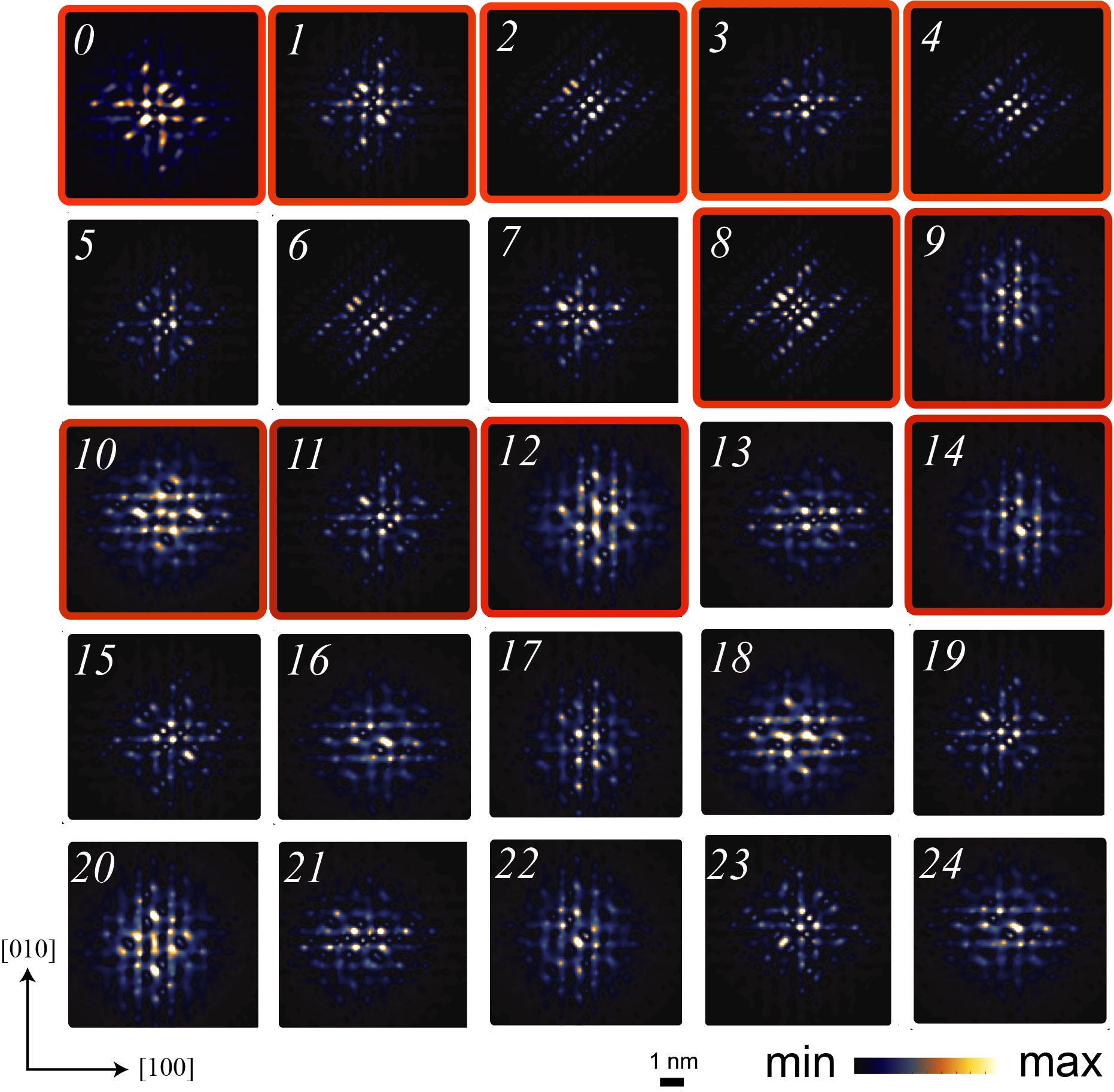
For a given target depth based on (), the dopant atoms are placed in the same plane. The in-plane positioning of the dopant atoms is shown in the Fig. 2(b). To demonstrate the working of the machine learning framework, we have selected four target depths: 4, 4.25, 4.5, 4.75, corresponding to =4 plane group. Due to the symmetry of the silicon crystal, the STM images exhibit same symmetry for other plane groups, therefore this particular set of planes at =4 represents all types of STM images which repeat for other values of Usman_NN_2016 . We have separately plotted six planes corresponding to =4. Note that for =0 and 1/4, we have only plotted one value of (1 and 3). The positions corresponding to =2 and 4 are at the other edge of the dimer rows and symmetrically similar to the positions at =1 and 3, respectively. This will result in exactly the same STM images, rotated by 270o. The exact positions corresponding to these images can be determined by overlaying dimer row atoms Usman_NN_2016 . In our classification scheme, we assume that one dopant atom is always at the center marked by =0. The second donor in the case of 2P will occupy one of the locations at the boundaries of the two diamonds with distances and 2 from the center dopant atom. These positions are labelled anti-clockwise from =1 to 8 for the inner diamond and =9 to 24 for the outer diamond as illustrated for ()=() in Figure 2 (b). Note that in each plane, the atom position at =0 is same as the value in that plane.
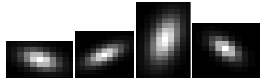
Based on the dopant locations plotted in Figure. 2(b), each dopant plane offers 25 possible configurations to place P/2P donor atoms, leading to 25 STM images. For the =4 plane group, we computed in total 125 STM images. Figure 2 (c) plots the STM images for one selected plane corresponding to =3/4 and =7. Each STM image is labelled with the corresponding value of . The STM images for the other five configurations are provided in the supplementary information Figures S1 to S5.
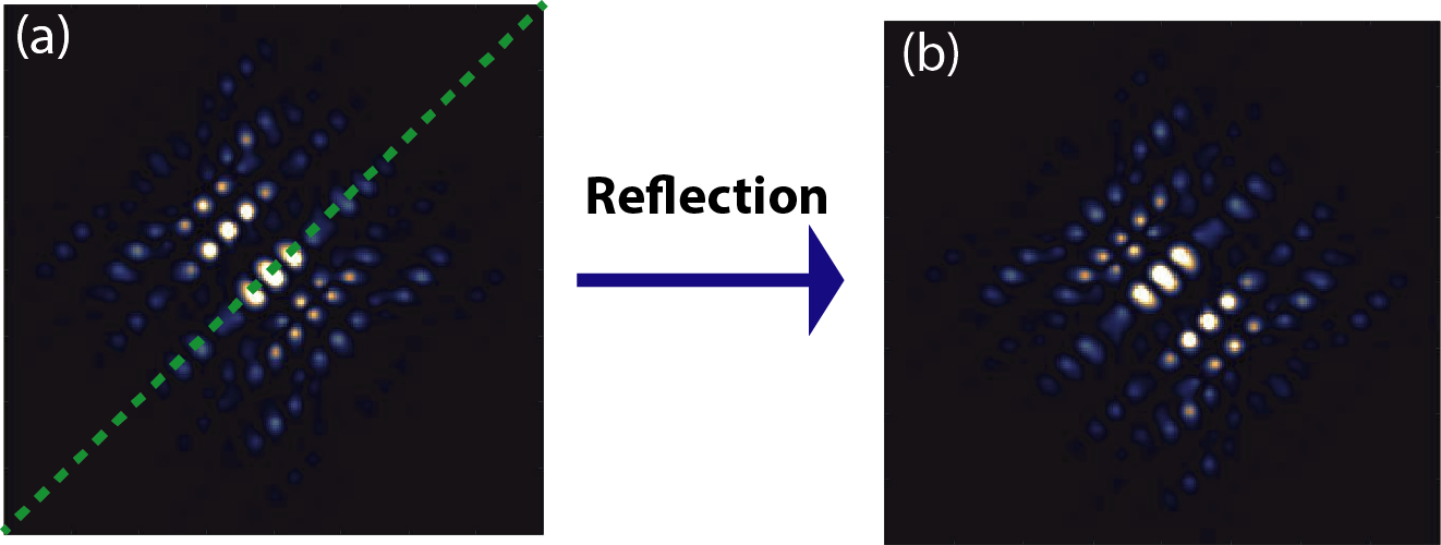
From Figure 2 (b), we note that a number of dopant positions are equivalent due to their symmetrical distance from the center location at =0. This implies that the corresponding STM images would also exhibit the same feature map with a possible rotation or reflection with respect to the axes parallel or normal to the dimer rows direction. For example, in Figure 2 (c), the images corresponding to =4 and =8 will be same if one of them is reflected with respect to the diagonal direction as shown in the supplementary information Figure S6. A careful examination of all images for () reveals that out of the 25 images, only 9 images are distinct. We classify the 25 images for the () group in 9 distinct image classes in the supplementary information Table T1. Further details about the classification of the STM images in distinct image classes is provided in the supplementary information section S1. Each class has been labelled by (), where is the minimum value of in that class. For =4, there are 50 distinct image classes. The 50 images representing the distinct classes are highlighted by the red color boundaries in Figure 2 (c) and also in the supplementary information Figures S1 to S5. The machine learning framework recognises dopant positions and count based on the feature maps, therefore it will only identify images with respect to these 50 classes. For example, in Figure 2 (c), the images corresponding to the positions = and 7 will be assigned to the same image class (). The determination of the exact dopant locations within an image class can be subsequently performed based on its relative symmetry with respect to the positions of the surface dimer rows, which can be done by overlaying dimer atom positions on top of the image.
Application of noise and image size reduction
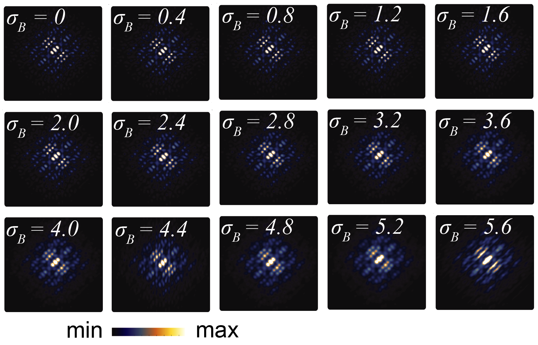
The computed STM images demonstrate a perfect symmetry and sharp bright features, whereas the published measured images Brazdova_PRB_2017 ; Salfi_NatMat_2014 ; Usman_NN_2016 may consists of features which are asymmetrical in brightness and/or blurred around the edges. In order to test the resiliency of the machine learning framework in the presence of feature asymmetry and blurriness, we artificially apply a range of two types of noise to the computed images. A planar noise () leads to an asymmetry of the features and a blurring noise () causes the features to spread across their edges, making adjacent features harder to distinguish. The computation of noise and its application to the exemplary images is provided in the supplementary information section S2. The supplementary information Figures S8 and S12 plot computed STM images as a function of various strengths of the planar and blurring noise, respectively. Based on the plotted images, we infer that 0.4 and 4.0 are the reasonable range of noise strengths beyond which the computed STM images become significantly distorted and cannot be accurately recognised. As part of the STM image preparation process, the application of noise is performed in the second step as illustrated in Figure 3 (a).
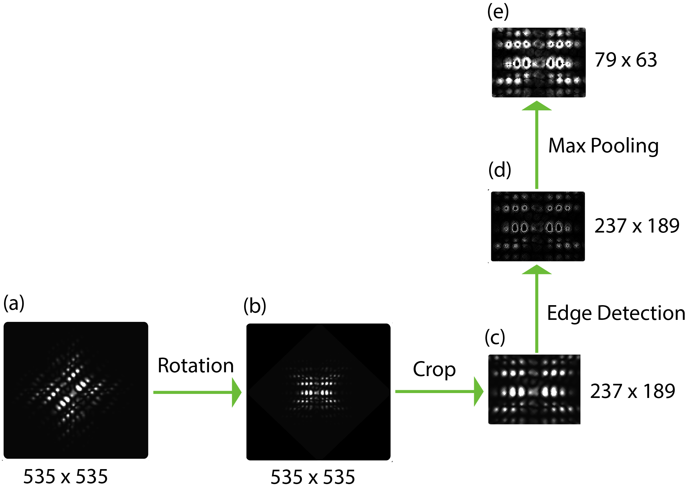
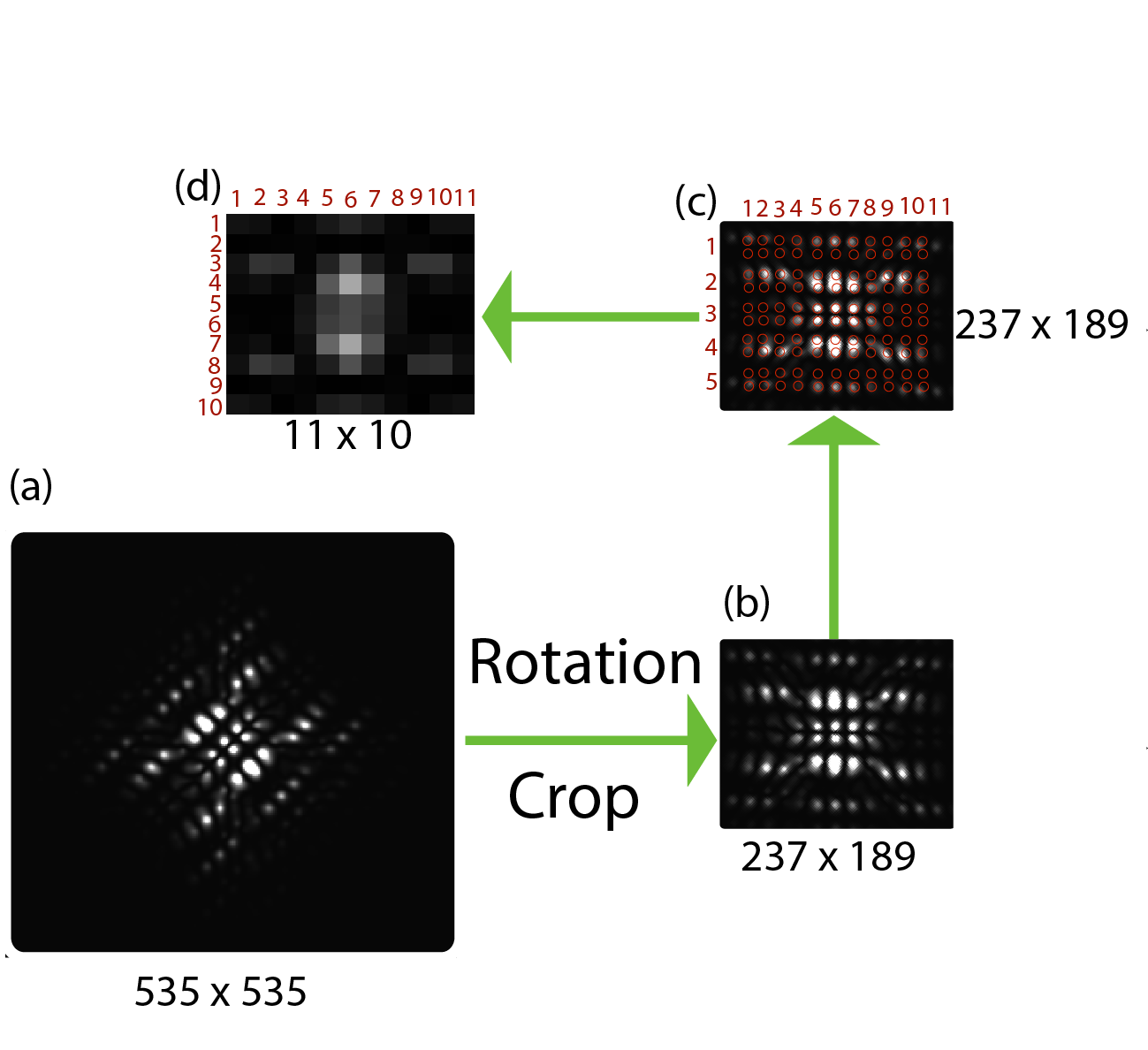
After the addition of noise, the computed STM images are further processed to reduce their size. The size of a computed image is 535535 pixels, which is quite large for the purpose of training and testing of a machine learning framework, which generally requires processing of several thousand images (105 training and 17600 test images in our study). To reduce the computational burden, we apply image reduction steps. Each coloured pixel represented by the RGB format is first converted to the grayscale format. We note that the STM images are computed over a large area (88 nm2), however the area around the features is dark indicating negligible tunnelling current. As the information about the donor positions is encoded in the bright features, we crop the dark region to further reduce the image sizes. This is done by first rotating the image clockwise by 45o degrees and then removing the pixels with the tunnelling current values below a threshold value. Further details of this process are provided in the supplementary information section S3 and S4, along with the supplementary Figures S13 and S14. At the end of this process, the image size is reduced from 535535 pixels to about 237189 pixels.
The information about the donor positions is present in the size, arrangement, and brightness of the image features. It is noted that each image consists of twenty to thirty bright features, which distinctly describe the corresponding position(s) and count of dopant atom(s). To further reduce the size of an image, we focus on the bright features and apply two techniques to extract the feature properties while preserving the donor position information. The first method which focuses on the shape of the features is called feature edges scheme in Figure 3 (a). Further details about this method are described in the supplementary information section S3. In this technique, we apply a filter operation which extracts the edges of the features. The image is then 33 sub-sampled or max-pooled to obtain a final image consisting of about 7963 pixels. Note that in this method, each image is of slightly different size based on number of features and their spatial distributions. Overall, the size of the computed images after the edge detection processing is always below 9090 for all the images studied in this work.
The second method is labelled as feature averages in Figure 3 (a) and is described in detail in the supplementary information section S4. In this scheme, we represent each feature by its overall average brightness with respect to the dimer positions. This drastically reduces the size of an image to 1110 pixels. Moreover, the size of the final processed images is also fixed for all cases. We do not apply any max-pooling function to feature averaged images. Following the image processing steps, we train and test a machine learning framework for both methods separately. A comparison is performed between the two image reduction schemes based on the computational efficiency and robustness against the application of noise.
Training of the convolutional neural network
The processed STM images are used to train a convolutional neural network (CNN). The robust training of a CNN generally requires a very large data set, typically consisting of sample spaces with sizes. We used ideal images and the images with various levels of planar noise () to train the CNN. To construct a sufficiently large training data set, we randomly vary between 0 and 0.4 and compute 2000 images corresponding to each of the 50 classes, accumulating a library of 105 training images. These images are separately processed through the edge detection and feature averaging schemes and are used to train two independent CNNs with one input, one hidden and one output layers.
Figure 3 (b) displays the work-flow of the CNN for the established high-throughput qubit characterisation scheme. Each image in the training data set is passed through the convolution layer before setting-up the CNN. In the case of the edge detection scheme, the CNN consists of a convolutional layer with 32, 33 kernels along with 22 max-pooling, followed by a hidden layer of 256 rectified linear units (ReLu) activated neurons. The images are scaled to 4848 pixels. Training on 105 images with 30 epochs achieved a learning accuracy of above 99.5% and completed in about 5 hours on an average desktop machine. For the case of the feature averaging scheme, a hidden layer of 64 ReLu activated neurons, and the training was performed on 105 images with 20 epochs, which was completed in about 30 minutes on an average desktop machine and resulted in a learning accuracy of 100%. In both cases, the output layer is densely connected layer with Softmax activation function. The CNN was compiled based on the Adam algorithm Kingma_arxiv_2017 with the learning rate of 10−4 and the categorical cross-entropy for optimization and as the loss function, respectively. The number of neurons is optimised by testing out various configurations of the CNN, and a sufficiently low number of neurons that will maintain the near perfect learning is chosen. The implementation of the CNN was performed by using Keras chollet2015keras , utilizing TensorFlow as the underlying platform tensorflow2015-whitepaper .
Qubit characterisation fidelities including noise
To test the performance of the machine learning framework, we define two parameters as the fidelity () of the qubit characterisation and the confidence level (). For a given test image, the trained CNN returns a set of 50 values (between 0 and 1), where each value indicates for that image to be in one of the 50 image classes. The test image is characterised as belonging to a particular image class based on the highest value. If the highest correctly identifies the image class, it is assigned a value of =1, otherwise =0. To test the robustness of the CNN, we prepared three separate test sets for both the edge detection and the feature averaging schemes. The first test set consists of 50 ideal STM images without the application of noise and the trained machine learning framework resulted in =1 with =1 for all images. This confirmed that the CNN has been properly trained based on the prepared training images.
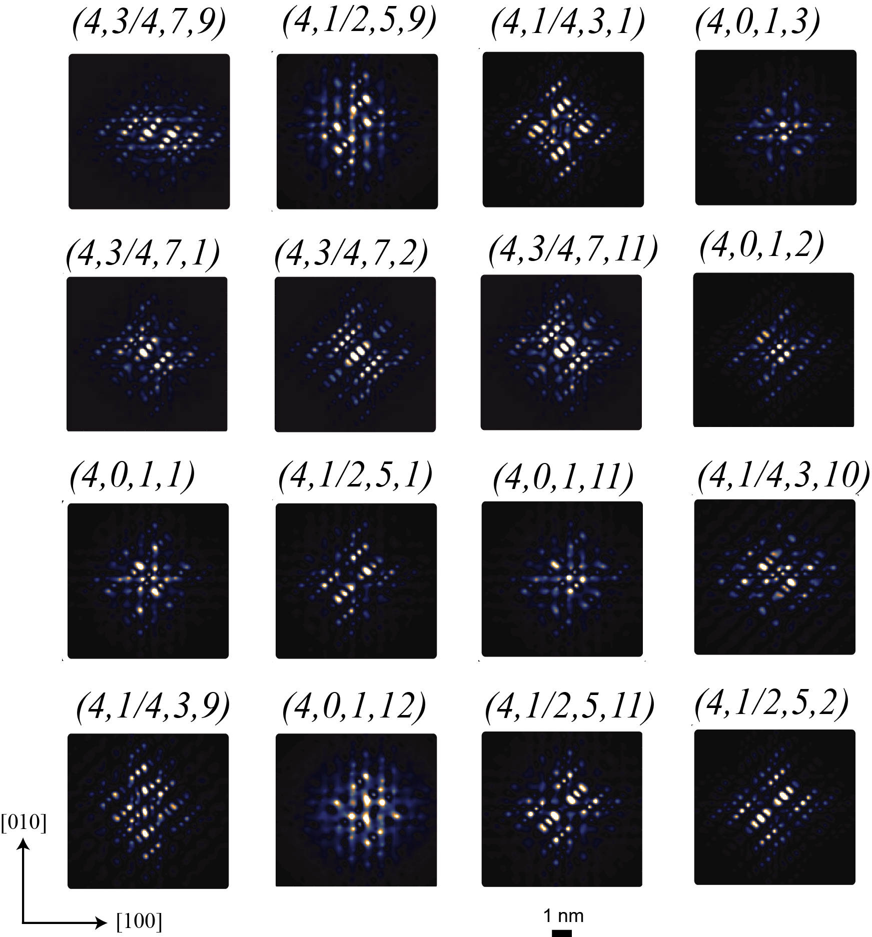
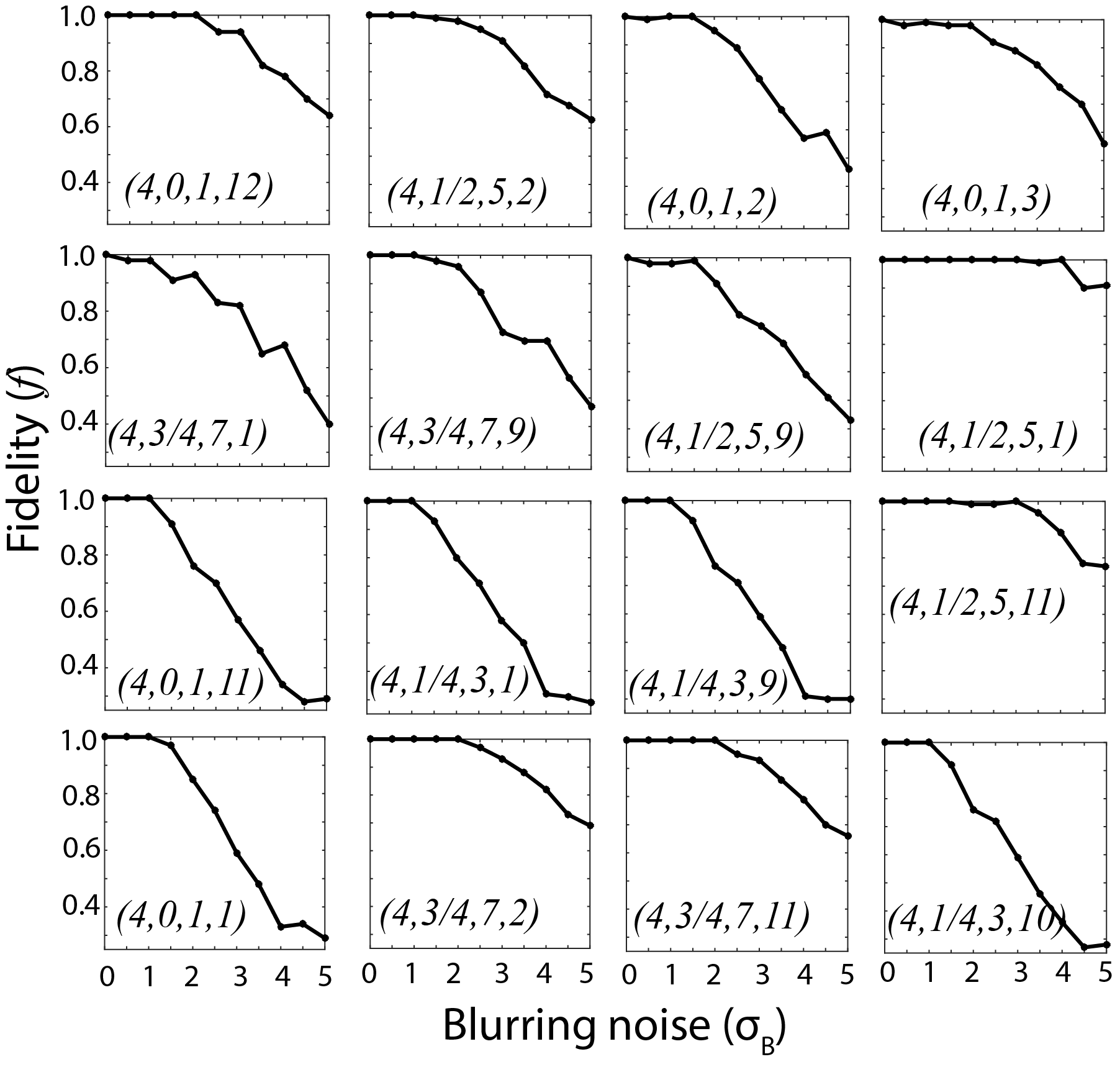
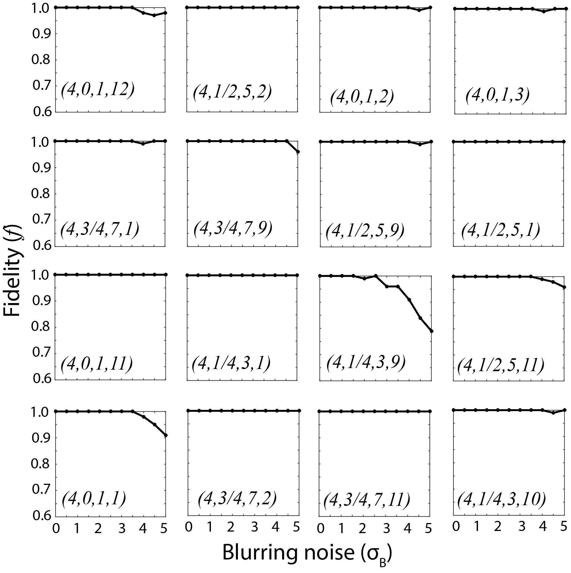
The second case consisted of test images after the application of blurring noise only for both the edge detection and the feature averaging schemes. To establish a sufficiently large test set, we arbitrarily selected 16 STM image classes (see supplementary information section S5 and Figure S15 for details) and applied the blurring noise () with its strength varying from 0 to 5.0 pixels with an increment of 0.5. At each value of , its orientation is randomly varied and 100 image are computed. The total test set consisted of 17600 STM images from the 16 classes. In the supplementary information Figures S16 and S17, we have plotted the % fidelity values (number of correctly classified images out of the 100 noisy images) obtained from the CNN for each image class independently. Figure 4 (a) plots the average values computed from the 1600 images (16 classes 100 noise orientations) at each value of the . The error bars indicate the standard error of the mean based on two standard deviations of the data. As expected, fidelities decrease when increases and the images become harder to recognise. Based on the plotted results, we infer that the feature averaging scheme provides much higher fidelities compared to the edge detection scheme for large values of . The higher fidelity values for the feature averaging scheme are also coupled with about an order of magnitude better computational efficiency and two orders of magnitude lower storage requirements. Therefore, we conclude that the feature averaging scheme offers superior performance for the established machine learning based qubit characterisation compared to the edge detection scheme. Interestingly, we find that the fidelity drop varies between different image classes and some images offer very high resiliency against the application of . This information may provide a useful input for the selection of a target depth during donor atom fabrication processes incorporating this autonomous characterisation scheme.
In the final test set, we simultaneously apply both planar and blurring noise to the set of STM images plotted in the supplementary information Figure S15. In the case of the edge detection scheme, we randomly vary noise orientation and strength from 0 0.4 and 0 2.0 range, whereas for the feature average scheme, we randomly vary noise levels from 0 0.4 and 0 4.0 due to its higher resiliency against the application of . The final processed images including noise are shown in Figure 4 (b) and (c). For both image-reduction schemes, the CNN characterises each image correctly (=1), with the values shown in the figure. Based on these results, we conclude that the CNN has been trained to accurately identify the STM images in the presence of both planar and blurring noise.
Summary and Outlook
In summary, this work takes a first step towards implementation of a machine learning framework for autonomous characterisation of a large-scale quantum computer architectures based on dopant impurities in silicon. The input to the established framework are simulated STM images of one electron wave functions confined on single dopants or on small clusters of closely-spaced dopants. The images are processed to optimise the exploitation of information known about the system (e.g. lattice geometry and surface dimers) and to reduce computational burden by developing and applying two feature-detection methods, namely edge detection and feature averages. Our results showed that both feature-detection methods enable high fidelity qubit characterisation at low noise level, with the feature averaging method providing considerably superior performance in the presence of large blurring noise. A convolutional neural network (CNN) is trained to characterise the noisy STM images and pinpoint the corresponding dopant atom position(s) and count with an exact lattice site precision. For the purpose of demonstrating the working of the established methods, the CNN was trained and tested on simulated STM images including noise levels commensurate with the published measurements. We note that the computed STM images have previously shown an extremely good agreement with the measured images at both pixel-by-pixel and feature-by-feature levels Usman_NN_2016 , therefore we expect that the trained CNN will be able to characterise experimental images with an accuracy equivalent to the simulated images with noise. As the training of CNN requires several thousand images, the capability to train based on simulated images eliminates the need for performing large scale experimental measurement, saving a lot of time and effort.
The established automated characterisation of atomic qubits with such a high level of accuracy will assist in the design and implementation of two-qubit quantum gates. The underpinning experimental expertise, the atomic-precision fabrication of dopant atoms in silicon via STM lithography Fuechsle_NN_2012 and the STM images of dopant wave functions by low-temperature tunnelling of single electron Salfi_NatMat_2014 , has already been demonstrated. Augmentation of the formulated machine learning setup with these experimental techniques is expected to enable high-throughput characterisation post-fabrication with minimal human interaction. We envision that as the number of qubits in quantum devices grows, the characterisation by direct quantum measurements will be increasingly onerous, and a fast, reliable and autonomous methodology may play a crucial role in the scale-up process.
Methods
Tight-binding wave function calculations
The computation of phosphorus dopant wave functions is performed by solving an atomistic sp3d5s∗ tight-binding Hamiltonian Boykin_PRB_2004 . The P donor atom is placed in a large silicon box consisting of roughly four million atoms. The confining potential on the P atom is represented by a comprehensive description of the central-cell effects, which include non-static dielectric screening of donor potential Usman_JPCM_2015 :
| (1) |
where A, , , and are fitting constants and have been numerically fitted as described in the literature Nara_JPSJ_1965 . Additionally, the nearest-neighbor bond-lengths of Si:P are strained by 1.9% in accordance with the recent DFT study Overhof_PRL_2004 . The value of U0 at the donor atom site is adjusted to empirically fit the binding energies of 1s manifold of states Usman_PRB_2015 . The calculation of wave functions also included the effect of 21 surface reconstruction, leading to the formation of dimer rows at the =0 surface Usman_NN_2016 ; Craig_SS_1990 . The impact of the surface strain due to the 21 reconstruction is included in the tight-binding Hamiltonian by a generalization of the Harrison’s scaling law, where the inter-atomic interaction energies are modified with the strained bond length as , where is the unperturbed bond-length of Si lattice and is a scaling parameter whose magnitude depends on the type of the interaction being considered and is fitted to obtain hydrostatic deformation potentials Boykin_PRB_2004 . The boundary conditions for the silicon box are selected as closed, with dangling bond energies shifted by large values to exclude their effect in the working range of energy Lee_PRB_2004 . The theoretical calculations were performed using the NEMO-3D framework Klimeck_2 ; Ahmed_Enc_2009 .
Computation of STM Images
The computation of the STM images is performed by coupling the atomistic tight-binding wave function calculation with the Bardeen’s tunnelling current formalism Bardeen_PRL_1961 . The wave function is decayed in the vacuum region above the reconstructed silicon surface based on the Slater orbital real-space representation Slater_PR_1954 . For the calculation of the tunnelling current, the dominant contribution has been found to come from the tip orbital Usman_NN_2016 , which is computed by applying the derivative rule reported by Chen Chen_PRB_1990 :
| (2) |
where is the donor wave function and is the position of the STM tip.
Each computed STM image is spanned over 88 nm2 area and consists of about 535535 pixels represented in the RGB color scheme.
Acknowledgements: This work was supported by the Australian Research Council (ARC) funded Center for Quantum Computation and Communication Technology (CE170100012), and partially funded by the USA Army Research Office (W911NF-08-1-0527). Computational resources were provided by the National Computing Infrastructure (NCI) and Pawsey Supercomputing Center through National Computational Merit Allocation Scheme (NCMAS).
Author contributions: LCLH conceived the initial idea, subsequently developed by all authors. MU and LCLH planned and supervised the project. MU and YZW computed and processed the STM images with input from LCLH. YZW, MU, and CDH formulated and applied the machine learning framework. All authors contributed in the discussions and analysis of the data. MU wrote the manuscript with inputs from all authors.
Data availability:
The data that support the findings of this study are available within the article and its supplementary information file. Further requests can be made to the corresponding author.
Additional information: The accompanied supplementary information document consists of 5 sections, 6 tables, and 17 figures. It provides additional STM images, a description of the feature-detection schemes, the implementation and application of noise, and benchmarking of the machine learning framework.
Competing financial interests: The authors declare no competing financial interests. A provisional patent application has been submitted based on aspects of this work.
Supplementary Information Document
Atomic-level Characterisation of Quantum Computer Arrays by Machine Learning
Muhammad Usman
Yi Z. Wong
Charles D. Hill
Lloyd C.L. Hollenberg
S1. Classification and symmetry analysis of STM images
Figure 2 (a) in the main text shows a small portion of the silicon crystal along with the atom position labels. Along the [001] direction, the Si lattice planes are divided into four plane groups (, where {0, 1/4, 1/2, 3/4}). Each plane group is a set of planes , whose depths from the =0 surface are given by: =(+), where =0,1,2,3,… Note that =(0,0) represents the =0 surface. Considering the periodicity of the dimers along the [-110] direction, two possible dopant locations per plane are defined by and , which repeat periodically in the lateral direction. The positions within the and groups are either directly underneath the dimers marked with green color or in-between the two dimers marked with red color. As the lateral positions within the and groups are always at the edges of the dimers, so these are equivalent with respect to the surface strain and therefore are marked by a single blue color. At =4, we highlight the atomic positions labelled with the corresponding values.
For the purpose of this study, we have considered qubits formed by either single phosphorus (P) atoms or a pair of P atoms that are closely-spaced as shown in the Figure 2 (a) and (b) of the main manuscript. The target depths are selected as 4, 4.25, 4.5, and 4.75 from the reconstructed silicon surface (corresponding to =4 group), where is the silicon lattice constant (0.543095 nm). Based on the symmetry of donor positions with respect to the surface dimer rows, the available locations for the P donor atoms are shown in Figure 2 (b) of the main manuscript. Each donor position is uniquely classified by 4 numbers (), where is the target plane depth group (i.e. 4 for this study), is the plane identifier (), is the atom number inside the group (1, 2, , 8) along the depth direction ([001]), and is the actual location of the P atoms for given () and varies from 0 to 24. The =0 label corresponds to a single donor atom (P) and 0 indicates two phosphorus atoms (2P), where the position of one P atom is always fixed at =0 and the second P atom is placed in one of the neighboring positions marked by =1,2,3, , 24. We should point out that this configuration, where qubits are formed by single donors or pairs of donors, is an exemplary case to demonstrate the working of our automated metrology. The technique is applicable for a large number of configurations, for example where donor clusters are made up of more than 2 closely spaced atoms, or where the donor positions within the cluster may vary along the [001] direction.
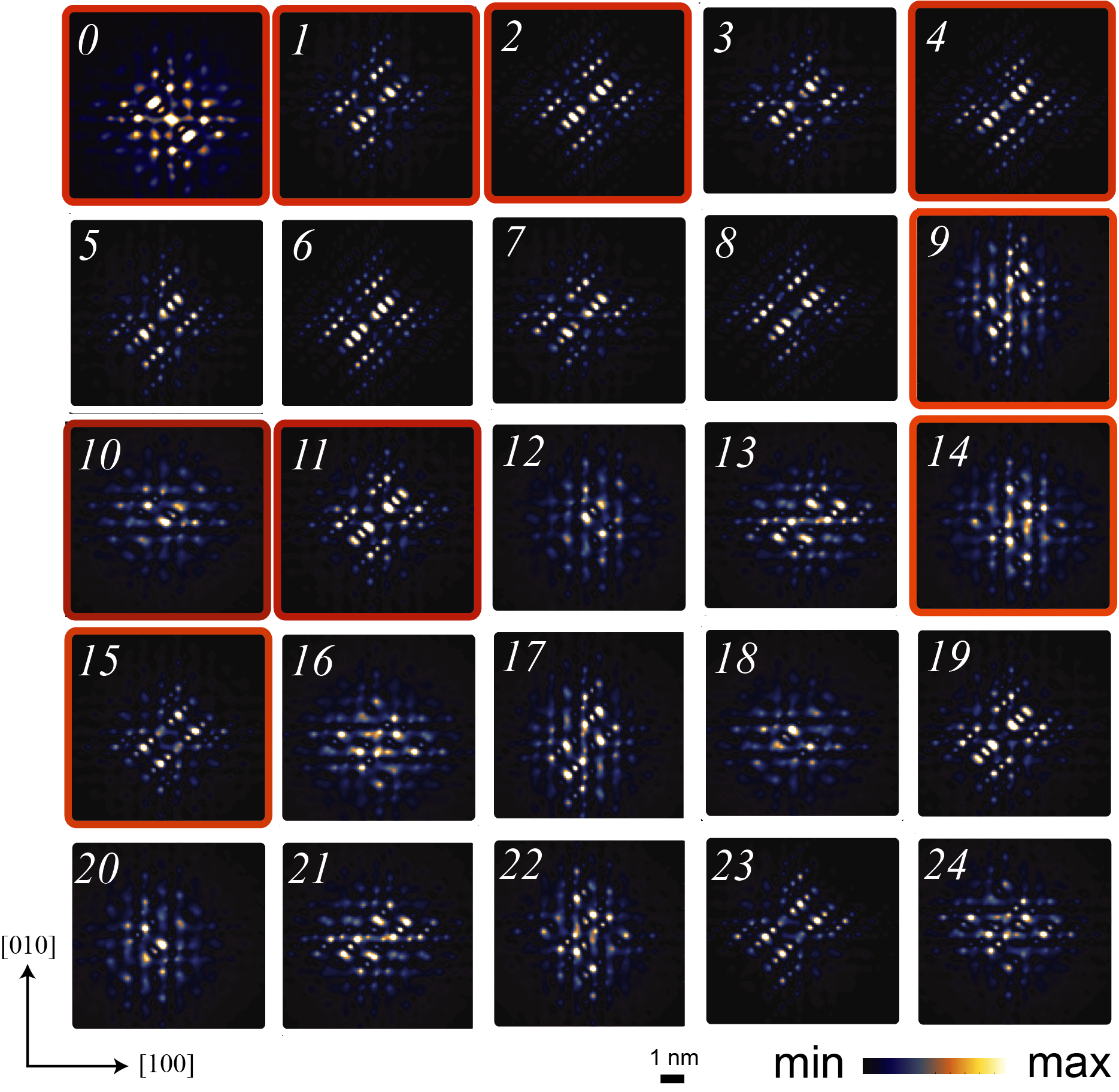
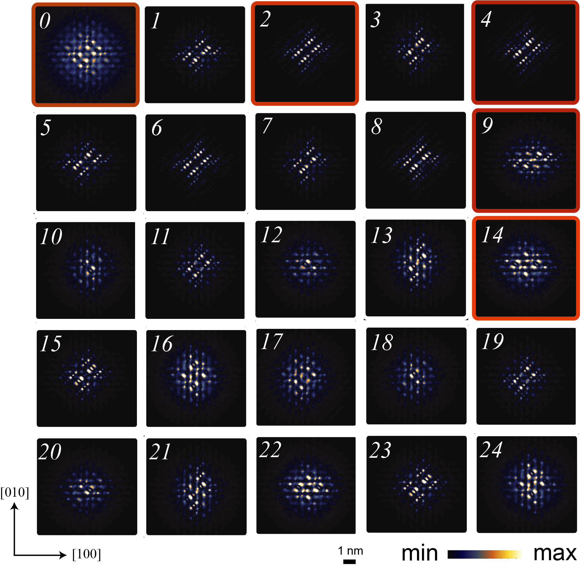
Figure 2 (c) in the main text shows all the STM images computed for =0,1,2,3, , 24 at () = (). The computed STM images for () equal to (), (), (), () and () are plotted in the Supplementary Figures S1 to S5, respectively.
Based on the symmetry of the silicon crystal, the atomic locations for phosphorus atoms are also symmetric with respect to the center position (=0). This leads to many of the STM images exhibiting the same symmetry and brightness of features, with rotation and/or reflection with respect to the axes parallel or perpendicular to the surface dimer rows. As an example, in the Supplementary Figure S6 (a), we have plotted an STM image for the donor position at () along with a green dotted line indicating the diagonal axis through the center of the image parallel to the dimer row direction. When this image is reflected along the green axis in part (b), it corresponds to the donor position at (). Therefore, we conclude that these two donor positions (() and ()) are identical with respect to the silicon crystal symmetry and lead to STM images with a similar feature distribution. In the Supplementary Figures S1 to S5, we have highlighted unique STM images by plotting red color boundaries and the other STM images are symmetry identical of these images. The machine learning framework will identify only one donor position for all the STM images that are symmetry identical. We can group such positions into a same image symmetry class. By carefully analyzing the symmetries of all the computed STM images, we have grouped them in the classes, where each class consists of images with same feature maps but within rotation and/or reflection operation. Supplementary Tables T1 to T6 provide classification of the STM images in unique image classes and also describe the relationship (symmetry, rotation and/or reflection) between the images within the same class. Based on this classification, we have identified in total fifty classes of unique STM images. The machine learning algorithm will be trained based on these fifty image classes. After training process, a test image will be identified based on a probability distribution consisting of fifty numbers, where each number represents the probability or confidence level () for a particular test image being in one of the fifty classes. The test image will be recognized and characterized based on the highest probability value (=1).
S2. Application of Noise
The theoretically computed STM images show bright features that are sharp and symmetrically distributed across or along the dimer row axes. However, the measured images reported in the literature Salfi_NatMat_2014 ; Usman_NN_2016 ; Brazdova_PRB_2016; Sinthiptharakoon_JPCM_2014 may exhibit features which are slightly asymmetrical and/or blurred close to the edges. To test the working of our machine learning technique in the presence of feature asymmetry and blurriness, we introduce artificial noise in the simulated images. Below, we briefly describe two methods that have been used in this work for the implementation and application of noise.
Planar Noise
The effect of asymmetry in the brightness of image features is captured by simulating a planar noise which is based on computing a two-dimensional function as follows:
| (3) |
Where , and are independently and randomly generated from a Gaussian distribution with =0 and set to various noise levels. Here, and are arbitrarily chosen to be close to the center of the image. A random sample of the contours of such a plane created by is shown in Supplementary Figure S7.
The resulting STM image including the planar noise can be simulated by using:
| (4) |
Where and are the computed STM images with and without the application of planar noise, respectively. The STM images for position () with various levels of the planar noise () are shown in the Supplementary Figure S8. The plotted images show that for 0.5, the images are severely cropped and hence do not represent a realistic condition. We therefore infer that a value of between 0 and 0.4 is reasonable to test the resiliency of our machine learning framework against the presence of planar noise.
The training set for the neural network requires a large number of STM images, therefore we included the planar noise in the training set by varying its magnitude randomly between 0.01 and 0.4. To create a reasonably large training set, we computed 2000 images per image class, producing a test set of 105 image for all of the 50 classes.
Blurring Noise
The other important difference between a theoretical and an experimental image may be the blurriness of the feature boundaries. The theoretical images always exhibit sharp and well-defined features, whereas an experimental image may consists of features which are slightly spread across their boundaries. In the traditional image processing techniques, blurriness is defined as the case where an image is not well-focused, and each pixel instead of being represented by a single sharp value is ‘mixed’ with neighboring pixels. Such blurring of a sharp image may be simulated via a process of Gaussian blurring, in which an image is convoluted with a kernel that represents a 2D Gaussian distribution with the peak at the center:
| (5) |
Where and represents the horizontal and vertical displacement of an element from the center of the kernel respectively, represents the level of blurriness in terms of pixels, and N is the normalization factor to ensure the sum of all elements in the kernel add up to one, such that the resulting blurred image is neither brighter nor darker compared to the original image. The evaluation of the Gaussian blurring kernel is illustrated in the Supplementary Figure S9. As an example, Supplementary Figure S10 shows the kernel values along with the grayscale plot for a 99 kernel with =2.
The blurring can be made directional and randomized by first making the blurring kernel elliptical, and then rotate it at a random angle:
| (6) |
Where and are independently drawn from the Gaussian distribution of N(0, ), which when squared results in a distribution with 1 degree of freedom, and is drawn from a uniform distribution from [0, 2] which represents rotation of the ellipse. The kernels of a randomized Gaussian blurring with =3 are shown in the Supplementary Figure S11. The Supplementary Figure S12 plots the STM images corresponding to the () position after the application of various levels of blurring noise. Based on these plots, we estimate that a blurriness noise represented by 3.0 is reasonable to identify STM images with high fidelity and is also commensurate with the level of changes typically observed in the published measurements.
We should also mention here that in the preparation of the training data set, we only considered planar noise. However, the test images included both planner and blurring noise with randomly selected strengths.
S3. Edge detection reduction scheme
Supplementary Figure S13 shows the complete procedure applied for the STM image reduction in case of the edge detection scheme. As an example, an STM image corresponding to the () position is selected and converted to grayscale as shown in part (a). It can be noted that the bright features are present around the center region and a large portion of the image is dark, indicating negligible tunnelling current. The overall size of the image can be reduced by first rotating the image clockwise by 45o as shown in (b) and then cropping the dark pixels in the image as exhibited in (c). The cropping is done by setting a threshold value for the tunnelling current, below which the image pixels are removed. After these steps, the size of the image is reduced from 535535 pixels to 237189 pixels.
We further note that the information is stored in the size and shape of the bright features, therefore the extraction of feature edges will preserve the information about the underpinning donor positions. This step is performed by a mathematical convolution function with the following kernel SMZiou98edgedetection:
The convoluted image is plotted in (d). Finally, the size of image can be further reduced by applying a sub-sampling or max-pooling function. This function divides the pixel map into smaller sections and for each section, the maximum value is selected. The image after the application of a 33 max-pooling function is shown in (e) which consists of 7963 pixels. The overall reduction of the STM image size from 535535 pixels to 7963 pixels significantly improves the computational efficiency and storage requirements of the neural network in both training and testing phases. We should note here that the final size of the STM image (7963 pixels) is specific for this particular image selected as an example. Since each STM image consists of different size and number of features, the eventual size of the processed STM will vary from one image to the other image. Based on all the processed images, we found that the final image size is always below 9090 pixels.
S4. Feature averaging reduction scheme
The STM image reduction procedure for the feature averaging scheme is shown in the Supplementary Figure S14 for an exemplary image corresponding to the position (). The first two steps are same as previously described in the section S3 and are shown in the parts (a) and (b).
After the rotation and cropping of the STM image, we apply the feature averaging procedure. The idea behind this scheme is based on the fact that the image features, which contain the information about the underpinning donor positions are present on atomic positions at the dimer sites. As each feature is distinct in an image and the arrangement of the features is also unique between different donor positions, it is possible to significantly reduce the size of an STM image by only persevering average brightness of each feature based on dimer row atoms. This is done by first overlaying the image with dimer atom positions as shown in part (c). There are 1110 atom positions which roughly cover all of the visible bright features. Based on the inspection of the computed STM images, the bright features are around the dimer rows, and these features can be represented by simply finding the average brightness of each feature around each dimer atom. This procedure reduces the STM image size to only 1110 pixels. The image after the application of the feature averaging procedure is illustrated in the part (d). We note that in this image reduction scheme, we do not apply max-pooling operation.
S5. Training and testing of the convolutional neural network (CNN)
The implementation of the convolutional neural network (CNN) was performed by using Keras chollet2015keras with TensorFlow tensorflow2015-whitepaper as the back-end. For the edge detection scheme (described in the section S3 above), the processed STM images including the planar noise were used to train the CNN. The CNN consisted of a convolutional layer with 32, 33 kernels along with 22 max-pooling, followed by a hidden layer of 256 rectified linear unit (ReLu) activated neurons as they offer better learning rate for the CNN. Training with 30 epochs yielded a nearly perfect learning and an accuracy of 100% for a test set consisting of STM images without the addition of noise.
In the case of the feature averaging scheme (described in the section S4 above), the CNN consisted of a hidden layer of 64 ReLu activated neurons. The training with 20 epochs led to nearly perfect learning and an accuracy of 100% for a test set consisting of STM images without the addition of noise. We note here that the number of neurons (256 and 64) are optimised by testing various different numbers, and by selecting the least number of neurons that maintain a near perfect learning.
After the training of the CNN, in the next phase, we performed its testing for the images with the application of random levels of noise described in the section S3 above. First, we evaluated the CNN fidelities with the introduction of blurring noise only for both the edge detection and feature averaging schemes. In this case, 16 STM images are arbitrarily chosen (shown in Figure S15), with 100 samples of each blurring level ranging from =0.5 to 5.0 at an increment of 0.5, establishing a test set of total 17600 images. The accuracy is measured based on the proportion of correct predictions out of the 100 samples. For each test image, the CNN returns a set of probability values indicating the probability of that image being in one of the particular image class. The Supplementary Figure S16 and S17 show the graphs of fidelities as a function of the applied blurring level for each of the test class. For low values of , the CNN identifies STM images with nearly 100% accuracy for all the plotted classes. When the blurring noise increases, the accuracy of feature detection scheme is clearly higher than the edge detection scheme. We also note that the decrease in identification accuracy is dependent on the STM image class.
To perform a comparison between the performance of the two image reduction methods, we plot the average fidelities as a function of the blurring noise strength along with the sample standard deviation in the Figure 4(a) of the main text. This plot clearly shows that overall the feature averaging method has a better fidelity compared to the edge detection. This is also accompanied with significantly higher computational efficiency. Based on 105 training images and 17600 test images, we find that the feature averaging method takes about 30 minutes time, compared to about 3 hour’s time frame for the edge detection case on an average desktop machine. Overall, we conclude that the feature averaging method is a better choice for the training a CNN capable of spatial metrology of donor-based qubits in silicon.
To test the fidelities of the trained CNN for STM images perturbed by both planar and blurring noise, we apply both noise simultaneously to the STM images plotted in the Supplementary Figure S15. Each image is then processed according to both edge detection and feature averaging schemes. After the image processing, the final test images are plotted in Figures 4 (b) and (c) of the main text. In each case, the CNN identifies the donor positions with 100% accuracy and the corresponding values of the confidence level are also provided in the figure.


![[Uncaptioned image]](/html/1904.01756/assets/TableS1.png)
![[Uncaptioned image]](/html/1904.01756/assets/TableS2.png)
![[Uncaptioned image]](/html/1904.01756/assets/TableS3.png)
![[Uncaptioned image]](/html/1904.01756/assets/TableS4.png)
![[Uncaptioned image]](/html/1904.01756/assets/TableS5.png)
![[Uncaptioned image]](/html/1904.01756/assets/TableS6.png)
References
- (1) Kane, B. E. A silicon-based nuclear spin quantum computer. Nature 393, 133 (1998).
- (2) Loss, D. & Divincenzo, D. Quantum computation with quantum dots. Phys. Rev. A 57, 120 (1998).
- (3) Zwanenburg, F. et al. Silicon quantum electronics. Rev. Mod. Phys. 85, 961 (2013).
- (4) Fuechsle, M. et al. A single-atom transistor. Nature Nanotechnology 7, 242 (2012).
- (5) Salfi, J. et al. Valley filtering in spatial maps of coupling between silicon donors and quantum dots. Phys. Rev. X 8, 031049 (2018).
- (6) Pla, J. et al. A single-atom electron spin qubit in silicon. Nature 489, 541 (2012).
- (7) Morello, A. et al. Single-shot readout of an electron spin in silicon. Nature 467, 687 (2010).
- (8) Tyryshkin, A. et al. Electron spin coherence exceeding seconds in high-purity silicon. Nature Materials 11, 143 (2012).
- (9) Saeedi, K. et al. Room-temperature quantum bit storage exceeding 39 minutes using ionized donors in silicon-28. Science 342, 830 (2013).
- (10) Pica, G., Lovett, B. W., Bhatt, R. N., Schenkel, T. & Lyon, S. A. Surface code architecture for donors and dots in silicon with imprecise and nonuniform qubit couplings. Phys. Rev. B 93, 035306 (2016).
- (11) Wang, Y., Chen, C.-Y., Klimeck, G., Simmons, M. & Rahman, R. Characterizing si:p quantum dot qubits with spin resonance techniques. Scientific Reports 6, 31830 (2016).
- (12) Testolin, M., Hill, C., Wellard, C. & Hollenberg, L. A precise cnot gate in the presence of large fabrication induced variations of the exchange interaction strength. Phys. Rev. A 76, 012302 (2007).
- (13) Hill, C. Robust controlled-not gates from almost any interaction. Phys. Rev. Lett. 98, 180501 (2007).
- (14) Butler, K., Davies, D., Cartwright, H., Isayev, O. & Walsh, A. Machine learning for molecular and materials science. Nature 559, 547 (2018).
- (15) Luna, P., Wei, J., Bengio, Y., Aspuru-Guzik, A. & Sargent, E. Use machine learning to find energy materials. Nature 552, 23 (2017).
- (16) Libbrecht, M. & Noble, W. Machine learning applications in genetics and genomics. Nature Reviews Genetics 16, 321 (2015).
- (17) Murphy, R. An active role for machine learning in drug development. Nature Chemical Biology 7, 327 (2011).
- (18) Heureux, A., Grolinger, K., Elyamany, H. & Capretz, M. Machine learning with big data: Challenges and approaches. IEEE Access 5, 7776 (2017).
- (19) Rashidi, M. & Wolkow, R. Autonomous scanning probe microscopy in situ tip conditioning through machine learning. ACS Nano 12 (6), 5185 (2018).
- (20) Rashidi, M. et al. Autonomous atomic scale manufacturing through machine learning. arXiv:1902.08818 (2019).
- (21) Bishop, C. M. Pattern recognition and machine learning (springer, 2006).
- (22) Salfi, J. et al. Spatially resolving valley quantum interference of a donor in silicon. Nature Materials 13, 605 (2014).
- (23) Usman, M. et al. Spatial metrology of dopants in silicon with exact lattice site precision. Nature Nanotechnology 11, 763 (2016).
- (24) Sinthiptharakoon, K. et al. J. Phys.: Condens. Matter 26, 012001 (2014).
- (25) Garleff, J. K. et al. Phys. Rev. B 78, 075313 (2008).
- (26) Ishida, N. et al. Direct visualization of the n impurity state in dilute ganas using scanning tunneling microscopy. Nanoscale 7, 16773 (2015).
- (27) Plantenga, R. et al. Spatially resolved electronic structure of an isovalent nitrogen center in gaas. Phys. Rev. B 96, 155210 (2017).
- (28) Krammel, C. et al. Incorporation of bi atoms in inp studied at the atomic scale by cross-sectional scanning tunneling microscopy. Phys. Rev. Materials 1, 034606 (2017).
- (29) Brazdova, V. et al. Exact location of dopants below the si(001):h surface from scanning tunneling microscopy and density functional theory. Phys. Rev. B 95, 075408 (2017).
- (30) Usman, M., Voisin, B., Salfi, J., Rogge, S. & Hollenberg, L. C. L. Towards visualisation of central-cell-effects in scanning tunnelling microscope images of subsurface dopant qubits in silicon. Nanoscale 9, 17013 (2017).
- (31) Wang, Y. et al. Highly tunable exchange in donor qubits in silicon. npj Quantum Information 2, 16008 (2016).
- (32) Pakkiam, P. et al. Single-shot single-gate rf spin readout in silicon. Phys. Rev. X 8, 041032 (2018).
- (33) Usman, M. et al. Donor hyperfine stark shift and the role of central-cell corrections in tight-binding theory. J. Phys.: Cond. Matt. 27, 154207 (2015).
- (34) Bardeen, J. Tunnelling from a many-particle point of view. Phys. Rev. Lett. 6, 57 (1961).
- (35) Chen, C. J. Tunneling matrix elements in three-dimensional space: The derivative rule and the sum rule. Phys. Rev. B 42, 8841 (1990-I).
- (36) Kingma, D. & Ba, J. Adam: A method for stochastic optimization. arXiv:1412.6980v9 (2017).
- (37) Chollet, F. et al. Keras. https://github.com/fchollet/keras (2015).
- (38) Abadi, M. et al. TensorFlow: Large-scale machine learning on heterogeneous systems (2015). URL https://www.tensorflow.org/. Software available from tensorflow.org.
- (39) Boykin, T. B., Klimeck, G. & Oyafuso, F. Valence band effective-mass expressions in the sp3d5s* empirical tight-binding model applied to a si and ge parametrization. Phys. Rev. B 69, 115201 (2004).
- (40) Nara, H. Screened impurity potential in si. J. Phys. Soc. Jap. 20, 778 (1965).
- (41) Overhof, H. & Gerstmann, U. Ab initio calculation of hyperfine and superhyperfine interactions for shallow donors in semiconductors. Phys. Rev. Lett. 92, 087602 (2004).
- (42) Usman, M. et al. Strain and electric field control of hyperfine interactions for donor spin qubits in silicon. Phys. Rev. B 91, 245209 (2015).
- (43) Craig, B. I. & Smith, P. V. The structure of the si(100)2 × 1: H surface. Surface Science 226, L55 (1990).
- (44) Lee, S., Oyafuso, F., von Allmen, P. & Klimeck, G. Boundary conditions for the electronic structure of finite-extent embedded semiconductor nanostructures. Phys. Rev. B 69, 045316 (2004).
- (45) Klimeck, G. et al. IEEE Trans. Elect. Dev. 54, 2090 (2007).
- (46) Ahmed, S. et al. Multimillion atom simulations with nemo 3-d. Springer Encyclopedia of Complexity and Systems Science ed R A Meyers (Heidelberg: Springer) p5745–83 (2009).
- (47) Slater, J. C. & Koster, G. F. Simplified lcao method for the periodic potential problem. Phys. Rev. 94, 1498 (1954).