From atomic layer to the bulk: low-temperature atomistic structure,
ferroelectric and electronic properties of SnTe films
Abstract
SnTe hosts ferroelectricity that competes with its weak non-trivial band topology: in the high-symmetry rocksalt structure –in which its intrinsic electric dipole is quenched– this material develops metallic surface bands, but in its rhombic ground-state configuration –that hosts a non-zero spontaneous electric dipole– the crystalline symmetry is lowered and the presence of surface electronic bands is not guaranteed. Here, the type of ferroelectric coupling and the atomistic and electronic structure of SnTe films ranging from 2 to 40 ALs are examined on freestanding samples, to which atomic layers were gradually added. 4 AL SnTe films are antiferroelectrically-coupled, while thicker freestanding SnTe films are ferroelectrically-coupled. The electronic band gap reduces its magnitude in going from 2 ALs to 40 ALs but it does not close due to the rhombic nature of the structure. These results bridge the structure of SnTe films from the monolayer to the bulk.
I Introduction
IV-VI compounds can form bulk rocksalt, orthorhombic or rhombic ground state structures depending on their average atomic number:Littlewood (1980a) PbS is a textbook example of rocksalt structureKittel (1953) that lacks an electric dipole, SnSe is an orthorhombic layered compound with antiferroelectric coupling (labeled ) among successive layers,Tan et al. (2014); Zhao et al. (2014) and SnTe develops a ferroelectric coupling (labeled ) on its rhombic phase. Bulk SnTe is a well studied material that nevertheless continues to provide new Physical phenomena. Studies exist of its optical and electronic properties Vago and Barrow (1946); Brebrick (1963); Damon et al. (1963); Zemel et al. (1965); Riedl et al. (1966) that include magnetoresistanceBurke et al. (1965); Savage et al. (1972); Allgaier and Houston (1972); Okazaki et al. (2018), the influence of temperature on electron transportBurke and Riedl (1969), the evolution of theoretical Lin et al. (1967); Rogers (1968); Tung and Cohen (1969); Rabe and Joannopoulos (1985) and experimental Tsu et al. (1968); Kemeny and Cardona (1976); Littlewood et al. (2010) electronic band structure methodologies, the relation of carrier concentration and anomalous resistivity with the rhombic to rocksalt phase transition Kobayashi et al. (1976); Grassie et al. (1979); Katayama and Mills (1980), and superconductivity Allen and Cohen (1969); Hein and Meijer (1969).
Additionally, experimental studies of structural phase transitions on these diatomic ferroelectrics were performed with Mösbauer Keune (1974) and Raman spectroscopies Brillson et al. (1974); Shimada et al. (1977), neutron scatteringPawley et al. (1966); Scott (1974); Iizumi et al. (1975a); Bevolo et al. (1976); Knox et al. (2014); Li et al. (2014a) and x-ray photoemission Shalvoy et al. (1977); Knox et al. (2014); O’Neill et al. (2017). Theories that explain such transitions based on lattice dynamics have been developedCowley et al. (1969); Natori (1976); Littlewood (1980b); Bilz et al. (1982); Strauch and Becher (1987); Cowley (1996) with an emphasis on soft-phonon modes Gillis (1969); Gillis and Koehler (1972) and the corresponding softening of elastic constants Beattie (1969). The combination of a temperature-dependent thermal Damon (1966) and electronic conductivities Burke and Riedl (1969); Kobayashi et al. (1976); Grassie et al. (1979); Katayama and Mills (1980) make SnTe a model thermoelectric materialLi et al. (2014a, b). The rhombic structure and ferroelectric ordering of SnTe occurs at temperatures below 150 K with a lattice constant Å and a rhombic angle Littlewood (1980a); Madelung et al. (1998); Iizumi et al. (1975b); Littlewood (1980c); Sugai et al. (1977); Jantsch (1983); Brillson and Muldawer (1974) among lattice vectors.
A twist on recreating the parity anomaly by electronic band inversion on the group-IV-VI material familyFradkin et al. (1986); Pankratov (1987) culminated on a rediscovery of SnTe as a topological crystalline insulator later on Hsieh et al. (2012a); Tanaka et al. (2012). But having a rhombic symmetry, i.e., a lower symmetry than that of a rocksalt structure, its surface electronic states along the (100) direction must be gapped at low temperaturePlekhanov et al. (2014). Nowadays, the coupling among the temperature-dependent degrees of freedom discussed in previous paragraphs– electronic band structureLi et al. (2014c), thermoelectricityRameshti and Asgari (2016)– as well as discoveries of higher-order topologySchindler et al. (2018) continue to find their way to thick SnTe slabs.
At the same time, interest on ultrathin SnTe originated due to theoretical predictions of ferroelectricity on these films Singh and Hennig (2014); Mehboudi et al. (2016); Huang et al. (2016); Kamal et al. (2016); Wu et al. (2017); Liu et al. (2018); Slawinska et al. (2019) and their experimental fabrication Chang et al. (2016, 2019). These SnTe slabs have not been created by capping a bulk sample, but grown from the bottom upChang et al. (2016); Zhang et al. (2014); Chang et al. (2019). And while common theoretical approaches assume a slab can be obtained by cutting two opposing surfaces of bulk rocksaltHsieh et al. (2012b) or rhombicPlekhanov et al. (2014); Wan et al. (2017); Liu et al. (2018) bulk samples, the present work is aimed to explore the structural evolution of a freestanding SnTe slab containing ALs by the successive addition of a 2 ALs in the overall lowest-energy conformation to the slab containing ALs with a positive integer, complementing the experimental results of Ref. Chang et al., 2019.
Toward this goal, the following points will be established here: (a) 4 AL SnTe films are antiferroelectrically coupled, while thicker suspended SnTe films turned out to be ferroelectrically coupled. (b) In going from 2 to 40 ALs, the rhombic angle , defined as , decreases from about down to , which is close to its experimental magnitude in the bulk. The manuscript is structured as follows. Technical details are provided in Sec. II, followed by results and discussion in Sec. III and conclusions in Sec. IV.
II Technical details
We performed ab-intio calculations with the SIESTA codeSoler et al. (2002) (that employs localized numeric atomic orbitalsJunquera et al. (2001) and norm-conserving Troullier-Martins pseudopotentialsTroullier and Martins (1991)) with van der Waals corrections of the Berland-Per Hyldgaard (BH) typeHyldgaard et al. (2014) (and also known as cx-vdW-DF1) as implemented by Román-Pérez and Soler,Román-Pérez and Soler (2009) on pseudopotentials whose radii were optimized in-house.Rivero et al. (2015a) The real-space grid in which the Poisson equation is solved has a cutoff energy of 300 Ry. A Monkhorst-PackMonkhorst and Pack (1976) mesh of points was employed in calculations involving unit cells, and a point mesh for calculations on 1111 supercells containing vacancies. Standard (DZP) basis setsJunquera et al. (2001) with a PAO.Energyshift flag of 0.002205 Ry were used. The vertical vacuum among periodic slabs was set to 60 Å, and dipole corrections were turned on. Structural optimizations were performed with a force tolerance of eV/Å. Spin-orbit coupling was turned on only after the electronic structure was optimized. Simulated STM imagesTersoff and Hamann (1983); Tománek and Louie (1988) were obtained by adding the electronic densities of individual wave functions in an energy window consistent with experimental energy ranges, and captured 2.5 Å above the SnTe film (see Refs. He et al., 2010; Koepke et al., 2015; Rivero et al., 2015b).
In addition, ultra-thin SnTe films were grown on 6H-SiC(0001) substrates that were sublimated to host epitaxial graphene layersHass et al. (2008) employing substrate preparation and van der Waals molecular beam epitaxy methods described before.Chang et al. (2016, 2019) STM measurements were carried out at 4.7 K on an Unisoku USM1600 system. The Pt-Ir alloy tip was calibrated on the epitaxial silver islands grown on a Si(111) substrate, and d/d experiments were conducted with a signal recovery lock-in amplifier having a modulation frequency of 913 Hz. Sample growth and STM studies were performed in the same vacuum system without exposure to air.
III Results and discussion
III.1 Structure and STM images of ferroelectric 2 AL SnTe films
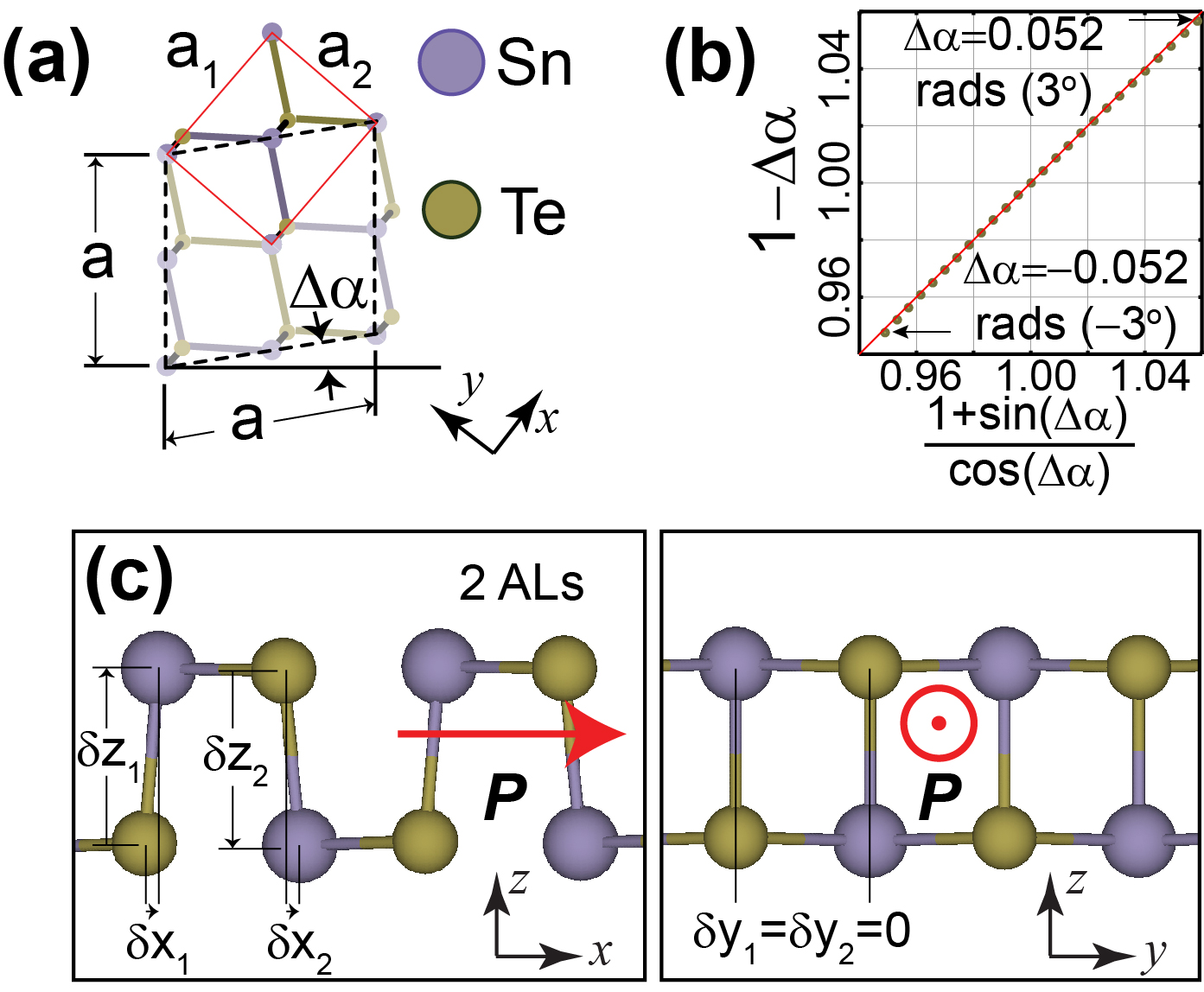
The rhombic distortion angle in Fig. 1(a) is related to the orthorhombic in-plane lattice parameters and by:Barraza-Lopez et al. (2018)
| (1) |
At low temperature and in ultra-thin films, SnTe displays values of no larger than which, as seen in Fig. 1(b), permits approximating as (in radians). Experimentally, the 2 AL SnTe film schematically shown in Fig. 1(c) registers a value at 4 K. In our calculations, Å and Å for . Figure 1(c) displays a side view of two unit cells of the 2 AL SnTe film, in which the direction of the intrinsic electric dipole is explicitly shown.
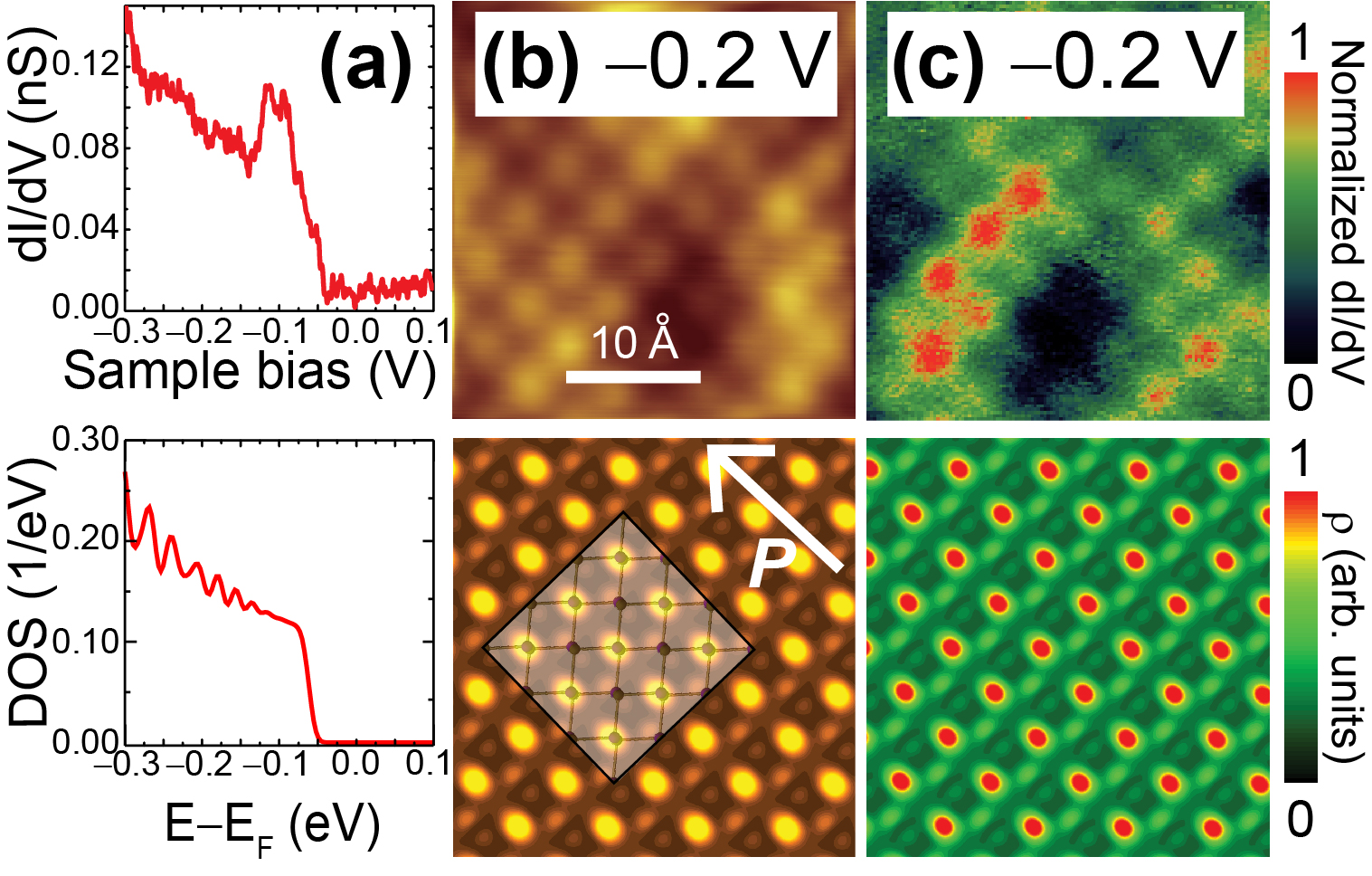
Experimental curves (upper panels) and simulated DOS data (lower panels) are presented for a 2 AL SnTe film in Fig. 2. The valence band edge on the DOS has been horizontally displaced to match the experimental band edge, so that simulated STM images are integrated to energies consistent with experiment. The experimental curve in Fig. 2(a) shows a peak at the band edge which does not appear on the simulated , and is likely due to adatoms at the graphene/2 AL SnTe interface, consistent with dark regions on the experimental figure that register a reduced tunneling current. Aside from that abrupt peak at about V, the experimental and simulated curves can be empirically related by .
The top subplot in Fig. 2(b) is an experimental topographic image in which the energy has been integrated down to V while the lower subplot corresponds to a simulation of the total density from the Fermi energy down to the corresponding experimental energy. Fig. 2(c), on the other hand, represents the electronic density within a narrow energy range; i.e., the density created by only a handful of electronic wavefunctions. Brightest spots that provide the atomic registry in Figs. 2(b,c) are reproduced in simulations. Bright spots in Figs. 2(b) and 2(c) correspond to the exposed Sn sublattice –which protrudes higher than the Te atoms according to Fig. 1(c)– as emphasized by an overlaid atomistic supercell in Fig. 2(b). In these plots, the brightest feature in all simulated images looks elongated along the direction parallel to .
III.2 On the possible type of atomic vacancies
To isolate vacancies and avoid spurious interactions arising from periodic images, a single structural defect (a Sn, Te, or Sn-Te dimer vacancy) was simulated on a 1111 supercell, making it computationally expensive to observe these defects on films thicker than 2 ALs. Nevertheless, STM images of structural vacancies display high contrast over many atomic sites and have geometrical shapes that ought to be independent of material thickness, giving us confidence that simulations of vacancies on a 2 AL SnTe film do provide relevant information that is representative of vacancies on thicker films.
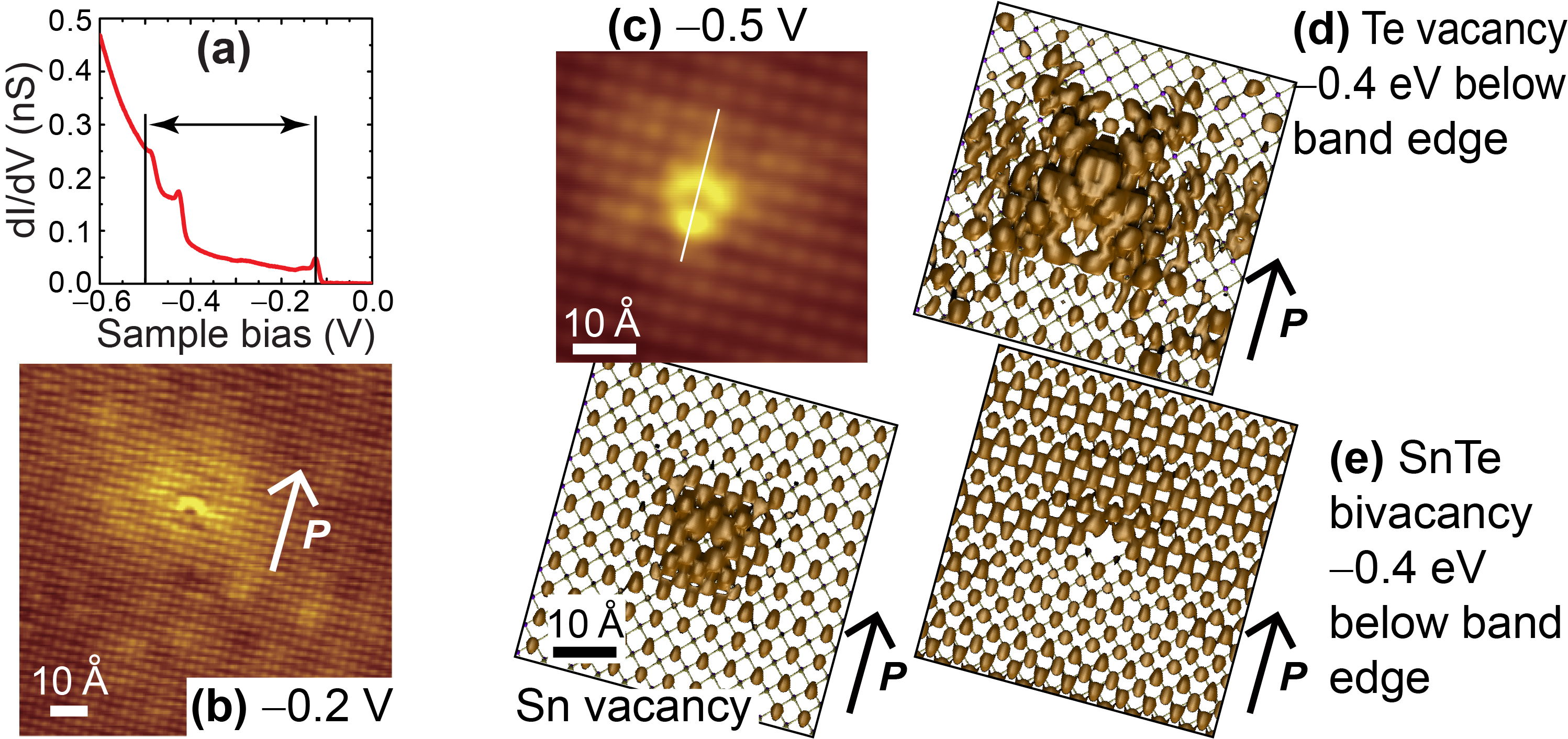
Figure 3(a) displays the experimental profile of a SnTe film of unknown thickness. The direction of the intrinsic electric dipole was obtained from the band bending at crystal edges (not shown in the Figure) using techniques developed before.Chang et al. (2016, 2019) The bright yellow feature in the STM topography image at V and = 100 pA in Fig. 3(b) will be shown to surround a Sn vacancy.
In Fig. 3(c), upper subplot, the topographic feature displayed in Fig. 3(a) is shown under a smaller bias of V and at a higher spatial resolution. The bright feature surrounding the dark spot is not radial-symmetric, and its axis of symmetry that is parallel to the arrow indicating the direction of in Fig. 3(b). Figure 3(c), lower subplot, is a simulated 3D isodensity image for a 2 AL SnTe film on the point mesh indicated before; this image was rotated to match the orientation and size of the experimental figure. A spot with no density centered along the Sn vacancy can be seen surrounded by an asymmetric density in the simulated image, with a larger (smaller) density above (below) the zero-density spot. In addition, the overall size of the simulated feature matches the size of the experimentally seen vacancy related state. The direction of the electric dipole can be directly observed from the simulated structure, and it matches the orientation of polarization determined experimentally.Chang et al. (2019)
A Te vacancy, seen in Fig. 3(d), has a features inconsistent with the experimental STM displayed in Fig. 3(c) at an energy and isodensity identical to that used in Fig. 3(c), implying that the experimentally observed feature is not a Te vacancy. Fig. 3(e) corresponds to the removal of the Sn atom from the upper sub-layer and the Te atom from the lower sub-layer. There, the bright-dark contrast is not as extended as in the case of the single Sn vacancy. In summary, the comparison among experiment and simulations allows us to affirm that the vacancies are due to Sn atoms which also dope the SnTe films with holes.
III.3 Antiferroelectrically-coupled 4 AL SnTe films
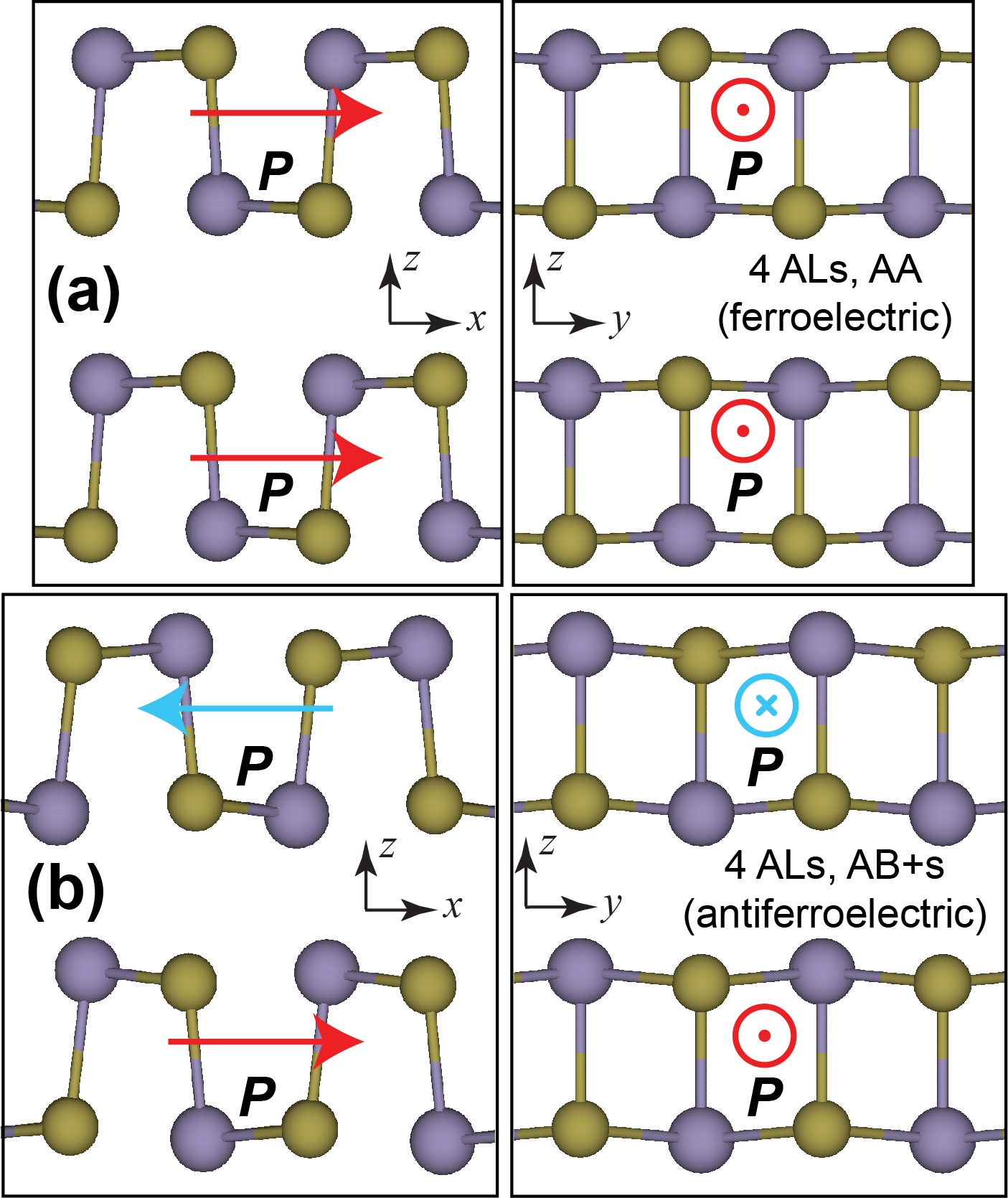
The ferroelectric coupling exemplified in Figs. 4(a) and 4(b) bears importance on electrostatic energy storage applications because antiferroelectrically-coupled ferroelectrics –such as the structure in subplot 4(b)– have been argued to lead to ultra-high-density capacitors.
Up to now, antiferroelectric coupling is induced by substitutional doping,Xu et al. (2017) making it relevant to know whether 4 AL SnTe realizes ferroelectric coupling –where consecutive pairs of 2 ALs have a parallel orientation of their in-plane polarization , c.f., Fig. 4(a)– or antiferroelectric behavior in which consecutive 2 ALs have antiparallel in-plane polarizations, c.f., Fig. 4(b).
There are three complementary experimental tests to determine the ferroelectric coupling of the 4 AL SnTe film:Chang et al. (2016) (i) the height profile, (ii) the band bending at the exposed ends, and the magnitude of from the Fourier transform of the STM image. Band bending is larger on a ferroelectrically-coupled (AA) 4 AL SnTe film when compared to an antiferroelectrically-coupled (AB) 4 AL SnTe film, because the electric field lines cancel out at the exposed edge on the latter case.Chang et al. (2016, 2019)
Here, we use energetics and the experimental values of for 2 AL and 4 ALs, to demonstrate an antiferroelectric coupling on 4 AL SnTe that is at odds with previous claims of ferroelectric couplingWan et al. (2017); Liu et al. (2018) and consistent with experiment.Chang et al. (2016, 2019)
In the present calculations, the structure shown in Fig. 4(a) has two 2 ALs relatively displaced along the direction. The structure shown in Fig. 4(b) and labeled (short for +shift) has the following coordinates:
| Sn | ||||
| Sn | ||||
| Te | ||||
| Te | ||||
| Sn | ||||
| Sn | ||||
| Te | ||||
with , , , and (all in Å) and , provided in Table 1.
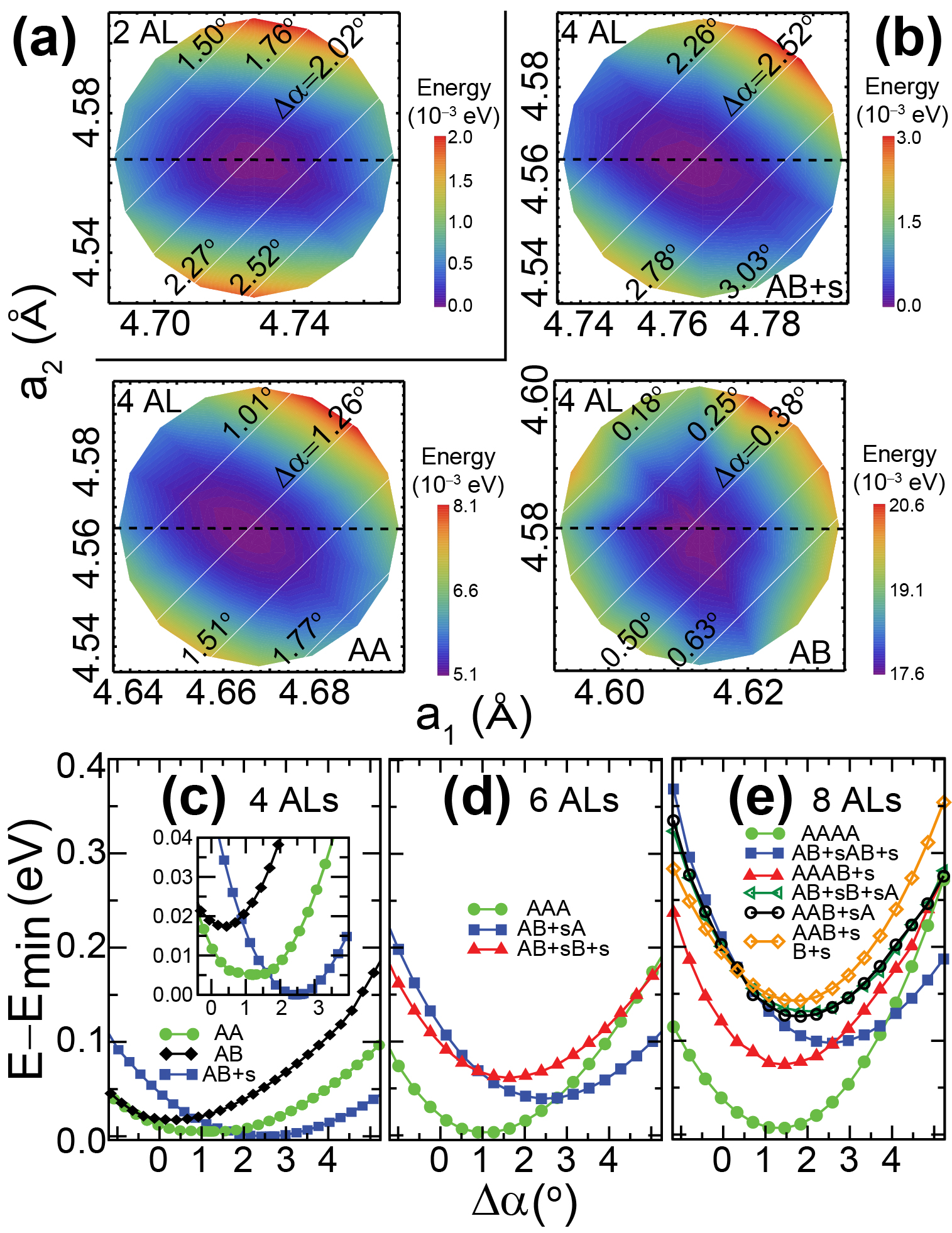
The structures shown in Figs. 1 and 4 are the result of a full structural optimization using a dense meshing procedure in which and are preset to fine mesh locations, and only atomic positions are relaxed. This procedure yields the energy versus , plots shown in Fig. 5(a), in which iso- lines oriented at 45∘ resulting from Eqn. 1 are displayed as well. The optimal lattice constants and relative energies are reported in Table 1 for each of these structures too. In this Table, the labels , and stand for ferroelectric coupling.
| Structure | (Å) | (Å) | Energy | ||
| theo. (∘) | expt. (∘) | diff. (eV) | |||
| 2 AL | 4.728 | 4.567 | |||
| 4 AL, | 4.668 | 4.566 | 1.28 | 0.0145 | |
| 4 AL, | 4.662 | 4.565 | 1.22 | 0.0150 | |
| 4 AL, | 4.766 | 4.565 | 2.52 | 0.0000 | |
| 6 AL, | 4.656 | 4.563 | 1.18 | ||
| 8 AL, | 4.651 | 4.564 | 1.09 |
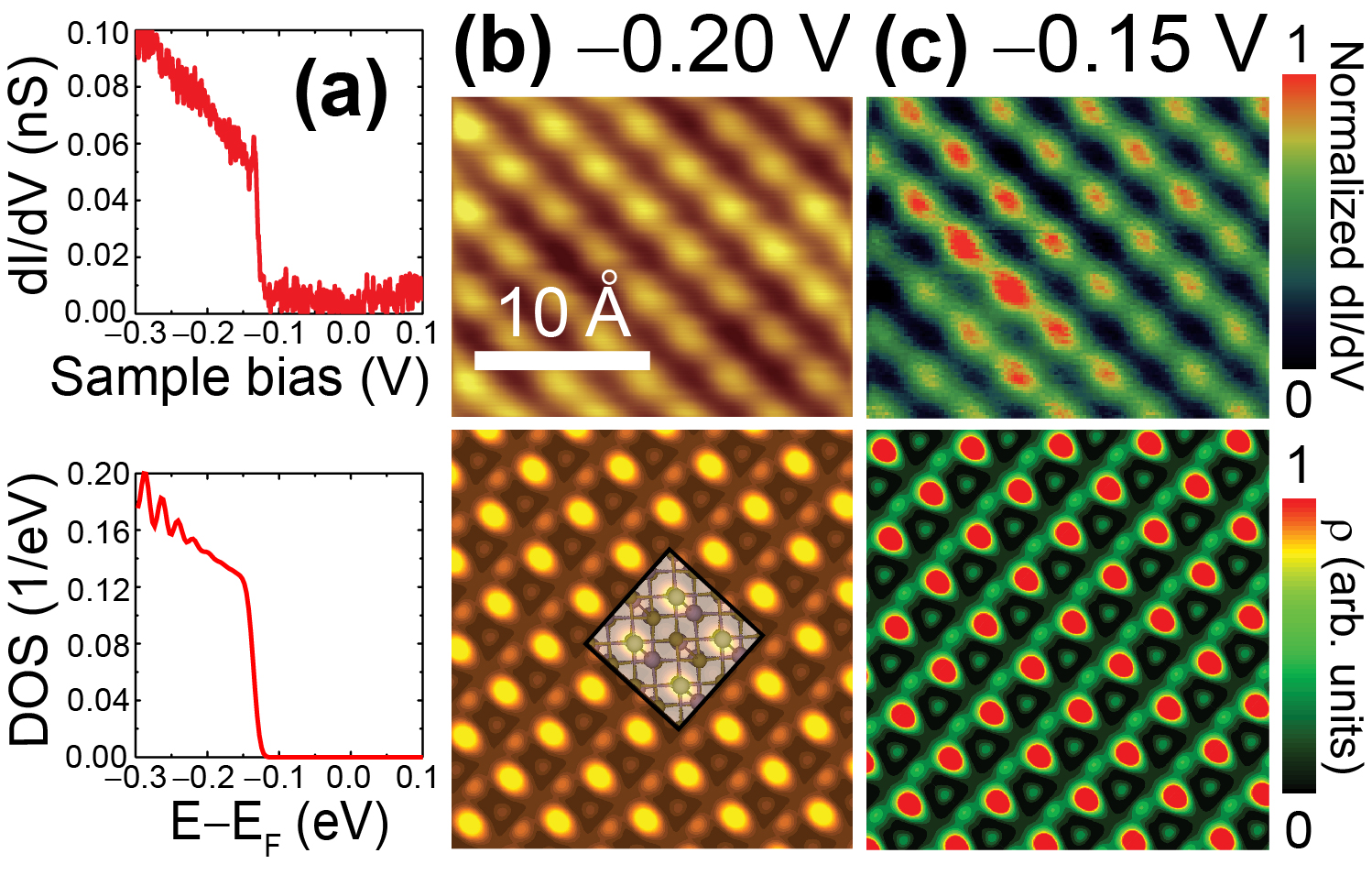
Figure 5(c) provides one-dimensional plots that cut across the paths that cross the absolute minima in Fig. 5(b). These plots provide a comparative study of energetics versus the relative placement of consecutive 2 ALs. The important point from Fig. 5 is that the lowest-energy 4 AL structure is antiferroelectrically coupled.
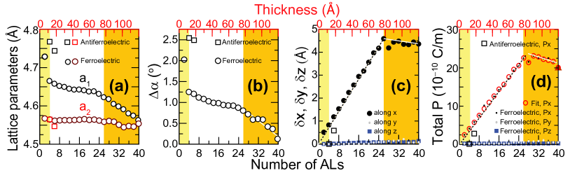
Fig. 6 displays experimental (upper row) and computational (lower row) results supporting the antiferroelectric coupling of 4 AL SnTe.Chang et al. (2019) There, the empirical relation (established in Fig. 2(a)) can be seen again. Furthermore, the location of bright spots between experimental and simulated STM images agree in subplots 6(b) and 6(c). Despite of the increased spatial resolution of the simulated STM image at V when compared with its experimental counterpart, Fig. 6(c), the dark diagonal feature can be observed along the elongated direction () in both images. Following Equation 1, such relative elongation of with respect to that leads to the asymmetric dark diagonal lines at is necessary to achieve the value experimental value of .
III.4 Atomistic structure and electronic bandstructures of thicker films
The antiferroelectric coupling of 4 AL SnTe and the ferroelectric coupling on the rhombic bulk discussed thus far imply the existence of a critical thickness at which the antiferroelectrically-coupled thin films transition onto a (bulk-like) ferroelectrically coupled SnTe.
Previous observation invites to examine the ferroelectric coupling of thicker films following the bottom-up approach pursued thus far. To this end, and as reported in Figs. 5(d) and 5(e), 6 AL SnTe slabs and 8 AL SnTe freestanding slabs were first considered, to find that ferroelectric coupling was preferred in both instances. For that reason, all thicker films studied here were stacked in a ferroelectric fashion consistent with bulk SnTe. Reference Zhang et al., 2014 indicates that films with a thickness in excess of 100 Å –corresponding to about 36 ALs– behave as bulk SnTe. Using such experimental guidance to set an upper thickness limit, the thickness dependence of in-plane lattice parameters and and for SnTe films ranging from 2 to 40 ALs as obtained computationally are shown in Figs. 7(a) and 7(b), respectively. Data in circles in Fig. 7 corresponds to a ferroelectric coupling among consecutive 2 ALs, while squares at the left ends of these plots describe slabs with an antiferroelectric coupling. The similar trends in between and in Figs. 7(a) and 7(b) arise from the linear dependency of on in Eqn. 1 and the almost-constancy of in Fig. 7(a).
There is an abrupt increase on and in going from 2 AL to 4 ALs, as the phase increases (squares in Figs. 7(a)), at the expense of reducing its dipole moment down to zero in 7(d). The area in white in Fig. 7(a) shows an almost constant , and a decay of by 0.0013 Å per AL, making in Fig. 7(b) decay by 0.025∘ per AL as the SnTe film gradually turns into a bulk structure. In between 30 and 40 ALs, the decay of in Fig. 7(a) becomes more drastic (0.0042 Å and 0.050∘ per AL, respectively), so that at 40 ALs in Fig. 7(b).
Atomistic displacements , and among anion and cations on a given 2 AL shown in Fig. 1 can be linked to the total polarization observed in these films. In order to characterize atomistic displacements for thicker films we define:
| (2) |
as the sum of displacements along the directions for thicker slabs, where is the number of ALs on a given slab (there are two displacements per 2 AL as seen in Fig. 1), with similar expressions for and . , and are displayed in Fig. 7(c). There, increases by 0.17 Å per AL up to 26 ALs, and then slightly decreases for thicknesses in between 28 and 40 ALs as a result of the sudden compression of seen in Fig. 7(a). In turn, and remain equal to zero.
In Fig. 7(d), we obtained the electric dipole of a 2 AL slab using the standard Berry phase approach,Resta and Vanderbilt (2007) and linked to the magnitude of . (We did so using VASP, with structures obtained from the SIESTA code.) This permitted adding the module on the standard Berry phase estimation to a periodic term that was consistent with the magnitude of . The total polarization increases by per AL up to 26 ALs. From then on, both and decrease at a rate of 0.02 Å per AL and per AL up to 40 ALs. The sudden drop of past 30 ALs does reduce the overall magnitude of despite of the subsequent addition of MLs, but it never brings the dipole all the way to zero for what it would be a rocksalt conformation. Instead, the reported non zero dipole is linked to the rhombic nature of films containing more than 4 ALs.
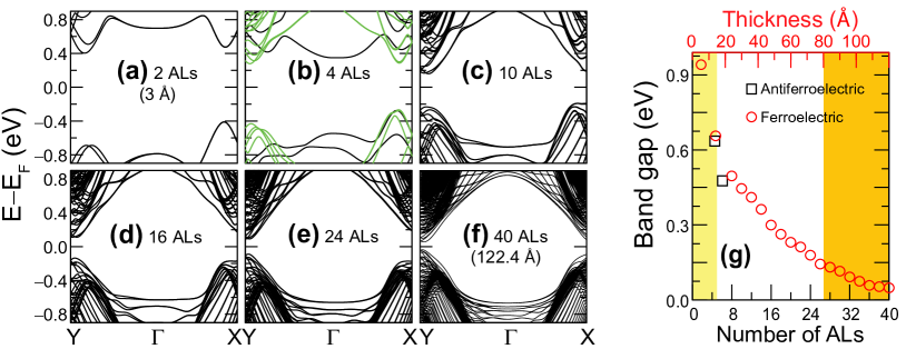
Lastly, we display the electronic structure with spin-orbit coupling (SOC) turned on of SnTe slabs with increasing thicknesses in Figs. 8(a-f). Figure 8(a) displays the 2 AL SnTe thin film as an indirect bandgap semiconductor.Gomes and Carvalho (2015) As seen in Fig. 8(b), such indirect bandgap remains for 4 AL SnTe with (black lines) and stacking (green lines) due to the largely dissimilar magnitudes of and in both structures. The indirect band gap persists up to 8 ALs.
Even though the band structure is not symmetric around the and points in Fig. 8(c), the band gap turns direct for a thickness of 10 ALs. Seeing the full sequence of subplots, Figs. 8(a-f), the band gap reduces its value as the thickness increases. This is emphasized by showing its magnitude in Fig. 8(g).
IV Conclusion
In conclusion, and despite of its longevity, SnTe remains an important material in Condensed Matter Physics, and the structural evolution of SnTe from 2 to 40 ALs has been provided here. 4 AL SnTe favors an antiferroelectric coupling, while suspended films with thicknesses ranging from 6 to 40 AL were ferroelectrically-coupled. The evolution of the rhombic distortion angle, the electric polarization, and of the electronic band structure have been provided as well. The atomistic structures and resulting electric dipole moments and electronic bandstructures are found to be different from those obtained by capping bulk structures, especially for ultrathin films. The information provided here is expected to better understand the coupling among atomistic structure and the fascinating material properties of SnTe.
Acknowledgements.
Research at Arkansas was supported by the U.S. Department of Energy, Office of Basic Energy Sciences, Division of Materials Science and Engineering under Early Career Award DE-SC0016139. Calculations were performed at the Center for Nanoscale Materials at Argonne National Laboratory. K.C. and S.S.P.P. were funded by the Deutsche Forschungsgemeinschaft (DFG, German Research Foundation) - Project number PA 1812/2-1. K.C., Q.-K.X., X.C. and S.-H.J. were supported by National Natural Science Foundation of China (Grant No. 51561145005) and Ministry of Science and Technology of China (Grant No. 2016YFA0301002).References
- Littlewood (1980a) P. B. Littlewood, J. Phys. C: Solid State Phys. 13, 4855 (1980a).
- Kittel (1953) C. Kittel, “Introduction to solid state physics,” (Wiley, NY, 1953) Chap. 1, p. 14, 1st ed.
- Tan et al. (2014) G. Tan, L.-D. Zhao, F. Shi, J. W. Doak, S.-H. Lo, H. Sun, C. Wolverton, V. P. Dravid, C. Uher, and M. G. Kanatzidis, J. Am. Chem. Soc. 136, 7006 (2014).
- Zhao et al. (2014) L.-D. Zhao, S.-H. Lo, Y. Zhang, H. Sun, G. Tan, C. Uher, C. Wolverton, V. P. Dravid, and M. G. Kanatzidis, Nature 508, 373 (2014).
- Vago and Barrow (1946) E. E. Vago and R. F. Barrow, Proc. Phys. Soc. 58, 707 (1946).
- Brebrick (1963) R. Brebrick, J. Phys. Chem. Solids 24, 27 (1963).
- Damon et al. (1963) D. H. Damon, C. R. Martin, and R. C. Miller, J. Appl. Phys. 34, 3083 (1963).
- Zemel et al. (1965) J. N. Zemel, J. D. Jensen, and R. B. Schoolar, Phys. Rev. 140, A330 (1965).
- Riedl et al. (1966) H. Riedl, R. Schoolar, and B. Houston, Solid State Comm. 4, 399 (1966).
- Burke et al. (1965) J. R. Burke, R. S. Allgaier, B. B. Houston, J. Babiskin, and P. G. Siebenmann, Phys. Rev. Lett. 14, 360 (1965).
- Savage et al. (1972) H. T. Savage, B. Houston, and J. R. Burke, Phys. Rev. B 6, 2292 (1972).
- Allgaier and Houston (1972) R. S. Allgaier and B. Houston, Phys. Rev. B 5, 2186 (1972).
- Okazaki et al. (2018) A. K. Okazaki, S. Wiedmann, S. Pezzini, M. L. Peres, P. H. O. Rappl, and E. Abramof, Phys. Rev. B 98, 195136 (2018).
- Burke and Riedl (1969) J. R. Burke and H. R. Riedl, Phys. Rev. 184, 830 (1969).
- Lin et al. (1967) P. Lin, W. Saslow, and M. L. Cohen, Solid State Communications 5, 893 (1967).
- Rogers (1968) L. M. Rogers, J. Phys. D: Appl. Phys. 1, 845 (1968).
- Tung and Cohen (1969) Y. W. Tung and M. L. Cohen, Phys. Rev. 180, 823 (1969).
- Rabe and Joannopoulos (1985) K. M. Rabe and J. D. Joannopoulos, Phys. Rev. B 32, 2302 (1985).
- Tsu et al. (1968) R. Tsu, W. E. Howard, and L. Esaki, Phys. Rev. 172, 779 (1968).
- Kemeny and Cardona (1976) P. C. Kemeny and M. Cardona, J. Phys. C: Solid State Phys. 9, 1361 (1976).
- Littlewood et al. (2010) P. B. Littlewood, B. Mihaila, R. K. Schulze, D. J. Safarik, J. E. Gubernatis, A. Bostwick, E. Rotenberg, C. P. Opeil, T. Durakiewicz, J. L. Smith, and J. C. Lashley, Phys. Rev. Lett. 105, 086404 (2010).
- Kobayashi et al. (1976) K. L. I. Kobayashi, Y. Kato, Y. Katayama, and K. F. Komatsubara, Phys. Rev. Lett. 37, 772 (1976).
- Grassie et al. (1979) A. D. C. Grassie, J. A. Agapito, and P. Gonzalez, J. Phys. C: Solid State Phys. 12, L925 (1979).
- Katayama and Mills (1980) S. Katayama and D. L. Mills, Phys. Rev. B 22, 336 (1980).
- Allen and Cohen (1969) P. B. Allen and M. L. Cohen, Phys. Rev. 177, 704 (1969).
- Hein and Meijer (1969) R. A. Hein and P. H. E. Meijer, Phys. Rev. 179, 497 (1969).
- Keune (1974) W. Keune, Phys. Rev. B 10, 5057 (1974).
- Brillson et al. (1974) L. J. Brillson, E. Burstein, and L. Muldawer, Phys. Rev. B 9, 1547 (1974).
- Shimada et al. (1977) T. Shimada, K. L. I. Kobayashi, Y. Katayama, and K. F. Komatsubara, Phys. Rev. Lett. 39, 143 (1977).
- Pawley et al. (1966) G. S. Pawley, W. Cochran, R. A. Cowley, and G. Dolling, Phys. Rev. Lett. 17, 753 (1966).
- Scott (1974) J. F. Scott, Rev. Mod. Phys. 46, 83 (1974).
- Iizumi et al. (1975a) M. Iizumi, Y. Hamaguchi, K. F. Komatsubara, and Y. Kato, J. Phys. Soc. Jpn. 38, 443 (1975a).
- Bevolo et al. (1976) A. J. Bevolo, H. R. Shanks, and D. E. Eckels, Phys. Rev. B 13, 3523 (1976).
- Knox et al. (2014) K. R. Knox, E. S. Bozin, C. D. Malliakas, M. G. Kanatzidis, and S. J. L. Billinge, Phys. Rev. B 89, 014102 (2014).
- Li et al. (2014a) C. W. Li, O. Hellman, J. Ma, A. F. May, H. B. Cao, X. Chen, A. D. Christianson, G. Ehlers, D. J. Singh, B. C. Sales, and O. Delaire, Phys. Rev. Lett. 112, 175501 (2014a).
- Shalvoy et al. (1977) R. B. Shalvoy, G. B. Fisher, and P. J. Stiles, Phys. Rev. B 15, 1680 (1977).
- O’Neill et al. (2017) C. D. O’Neill, D. A. Sokolov, A. Hermann, A. Bossak, C. Stock, and A. D. Huxley, Phys. Rev. B 95, 144101 (2017).
- Cowley et al. (1969) E. R. Cowley, J. K. Darby, and G. S. Pawley, J. Phys. C: Solid State Phys. 2, 1916 (1969).
- Natori (1976) A. Natori, J. Phys. Soc. Jpn. 41, 782 (1976).
- Littlewood (1980b) P. B. Littlewood, J. Phys. C: Solid State Phys. 13, 4875 (1980b).
- Bilz et al. (1982) H. Bilz, H. Büttner, A. Bussmann-Holder, W. Kress, and U. Schröder, Phys. Rev. Lett. 48, 264 (1982).
- Strauch and Becher (1987) D. Strauch and R. Becher, J. Phys. C: Solid State Phys. 20, 1641 (1987).
- Cowley (1996) E. Cowley, Physica A 232, 585 (1996).
- Gillis (1969) N. S. Gillis, Phys. Rev. Lett. 22, 1251 (1969).
- Gillis and Koehler (1972) N. S. Gillis and T. R. Koehler, Phys. Rev. B 5, 1925 (1972).
- Beattie (1969) A. G. Beattie, J. Appl. Phys. 40, 4818 (1969).
- Damon (1966) D. H. Damon, J. Appl. Phys. 37, 3181 (1966).
- Li et al. (2014b) C. W. Li, J. Ma, H. B. Cao, A. F. May, D. L. Abernathy, G. Ehlers, C. Hoffmann, X. Wang, T. Hong, A. Huq, O. Gourdon, and O. Delaire, Phys. Rev. B 90, 214303 (2014b).
- Madelung et al. (1998) O. Madelung, U. Rössler, and M. Schulz, eds., “Tin telluride (snte) crystal structure, lattice parameters,” in Non-Tetrahedrally Bonded Elements and Binary Compounds I (Springer Berlin Heidelberg, Berlin, Heidelberg, 1998) pp. 1–8.
- Iizumi et al. (1975b) M. Iizumi, Y. Hamaguchi, K. F. Komatsubara, and Y. Kato, J. Phys. Soc. Jpn. 38, 443 (1975b).
- Littlewood (1980c) P. B. Littlewood, J. Phys. C: Solid State Phys. 13, 4875 (1980c).
- Sugai et al. (1977) S. Sugai, K. Murase, and H. Kawamura, Solid State Commun. 23, 127 (1977).
- Jantsch (1983) W. Jantsch, “Dielectric properties and soft modes in semiconducting (Pb, Sn, Ge)Te,” in Dynamical Properties of IV-VI Compounds (Springer Berlin Heidelberg, Berlin, Heidelberg, 1983) pp. 1–50.
- Brillson and Muldawer (1974) L. Brillson and L. Muldawer, Phys. Rev. B 9, 1547 (1974).
- Fradkin et al. (1986) E. Fradkin, E. Dagotto, and D. Boyanovsky, Phys. Rev. Lett. 57, 2967 (1986).
- Pankratov (1987) O. Pankratov, Phys. Lett. A 121, 360 (1987).
- Hsieh et al. (2012a) T. H. Hsieh, H. Lin, J. Liu, W. Duan, A. Bansil, and L. Fu, Nature Commun. 3, 982 (2012a).
- Tanaka et al. (2012) Y. Tanaka, Z. Ren, T. Sato, K. Nakayama, S. Souma, T. Takahashi, K. Segawa, and Y. Ando, Nature Phys. 8, 800 (2012).
- Plekhanov et al. (2014) E. Plekhanov, P. Barone, D. Di Sante, and S. Picozzi, Phys. Rev. B 90, 161108 (2014).
- Li et al. (2014c) X. Li, F. Zhang, Q. Niu, and J. Feng, Sci. Rep. 4 (2014c), 10.1038/srep06397.
- Rameshti and Asgari (2016) B. Z. Rameshti and R. Asgari, Phys. Rev. B 94, 205401 (2016).
- Schindler et al. (2018) F. Schindler, A. M. Cook, M. G. Vergniory, Z. Wang, S. S. P. Parkin, B. A. Bernevig, and T. Neupert, Science Advances 4 (2018), 10.1126/sciadv.aat0346.
- Singh and Hennig (2014) A. K. Singh and R. G. Hennig, Appl. Phys. Lett. 105, 042103 (2014).
- Mehboudi et al. (2016) M. Mehboudi, A. M. Dorio, W. Zhu, A. van der Zande, H. O. H. Churchill, A. A. Pacheco-Sanjuan, E. O. Harriss, P. Kumar, and S. Barraza-Lopez, Nano Lett. 16, 1704 (2016).
- Huang et al. (2016) L. Huang, F. Wu, and J. Li, J. Chem. Phys. 144, 114708 (2016).
- Kamal et al. (2016) C. Kamal, A. Chakrabarti, and M. Ezawa, Phys. Rev. B 93, 125428 (2016).
- Wu et al. (2017) M. Wu, S.-H. Wei, and L. Huang, Phys. Rev. B 96, 205411 (2017).
- Liu et al. (2018) K. Liu, J. Lu, S. Picozzi, L. Bellaiche, and H. Xiang, Phys. Rev. Lett. 121, 027601 (2018).
- Slawinska et al. (2019) J. Slawinska, F. T. Cerasoli, H. Wang, S. Postorino, A. Supka, S. Curtarolo, M. Fornari, and M. B. Nardelli, 2D Mater. 6, 025012 (2019).
- Chang et al. (2016) K. Chang, J. Liu, H. Lin, N. Wang, K. Zhao, A. Zhang, F. Jin, Y. Zhong, X. Hu, W. Duan, Q. Zhang, L. Fu, Q.-K. Xue, X. Chen, and S.-H. Ji, Science 353, 274 (2016).
- Chang et al. (2019) K. Chang, T. P. Kaloni, H. Lin, A. B. Pinto, A. K. Pandeya, I. Kostanovskiy, K. Zhao, Y. Zhong, X. Hu, Q.-K. X. Xue, X. Chen, S.-H. Ji, S. Barraza-Lopez, and S. S. P. Parkin, Adv. Mater. 31, 1804428 (2019).
- Zhang et al. (2014) D. Zhang, H. Baek, J. Ha, T. Zhang, J. Wyrick, A. V. Davydov, Y. Kuk, and J. A. Stroscio, Phys. Rev. B 89, 245445 (2014).
- Hsieh et al. (2012b) T. H. Hsieh, H. Lin, J. Liu, W. Duan, A. Bansil, and L. Fu, Nat. Commun. 3, 982 (2012b).
- Soler et al. (2002) J. M. Soler, E. Artacho, J. D. Gale, A. García, J. Junquera, P. Ordejón, and D. Sánchez-Portal, J. Phys.: Condens. Matter 14, 2745 (2002).
- Junquera et al. (2001) J. Junquera, O. Paz, D. Sánchez-Portal, and E. Artacho, Phys. Rev. B 64, 235111 (2001).
- Troullier and Martins (1991) N. Troullier and J. L. Martins, Phys. Rev. B 43, 1993 (1991).
- Hyldgaard et al. (2014) P. Hyldgaard, K. Berland, and E. Schröder, Phys. Rev. B 90, 075148 (2014).
- Román-Pérez and Soler (2009) G. Román-Pérez and J. M. Soler, Phys. Rev. Lett. 103, 096102 (2009).
- Rivero et al. (2015a) P. Rivero, V. M. García-Suárez, D. Pereñiguez, K. Utt, Y. Yang, L. Bellaiche, K. Park, J. Ferrer, and S. Barraza-Lopez, Comput. Mater. Sci. 98, 372 (2015a).
- Monkhorst and Pack (1976) H. J. Monkhorst and J. D. Pack, Phys. Rev. B 13, 5188 (1976).
- Tersoff and Hamann (1983) J. Tersoff and D. R. Hamann, Phys. Rev. Lett. 50, 1998 (1983).
- Tománek and Louie (1988) D. Tománek and S. G. Louie, Phys. Rev. B 37, 8327 (1988).
- He et al. (2010) K. T. He, J. C. Koepke, S. Barraza-Lopez, and J. W. Lyding, Nano Lett. 10, 3446 (2010).
- Koepke et al. (2015) J. C. Koepke, J. D. Wood, C. M. Horvath, J. W. Lyding, and S. Barraza-Lopez, Appl. Phys. Lett. 107, 071603 (2015).
- Rivero et al. (2015b) P. Rivero, C. M. Horvath, Z. Zhu, J. Guan, D. Tománek, and S. Barraza-Lopez, Phys. Rev. B 91, 115413 (2015b).
- Hass et al. (2008) J. Hass, F. Varchon, J. E. Millán-Otoya, M. Sprinkle, N. Sharma, W. A. de Heer, C. Berger, P. N. First, L. Magaud, and E. H. Conrad, Phys. Rev. Lett. 100, 125504 (2008).
- Barraza-Lopez et al. (2018) S. Barraza-Lopez, T. P. Kaloni, S. P. Poudel, and P. Kumar, Phys. Rev. B 97, 024110 (2018).
- Xu et al. (2017) B. Xu, J. Íñiguez, and L. Bellaiche, Nat. Commun. 8, 15682 (2017).
- Wan et al. (2017) W. Wan, C. Liu, W. Xiao, and Y. Yao, Appl. Phys. Lett. 111, 132904 (2017).
- Resta and Vanderbilt (2007) R. Resta and D. Vanderbilt, “Physics of ferroelectrics,” (Springer, Berlin, 2007) pp. 31–68, 1st ed.
- Gomes and Carvalho (2015) L. C. Gomes and A. Carvalho, Phys. Rev. B 92, 085406 (2015).