High-mobility, wet-transferred graphene grown by chemical vapor deposition
Abstract
We report high room-temperature mobility in single layer graphene grown by Chemical Vapor Deposition (CVD) after wet transfer on SiO2 and hexagonal boron nitride (hBN) encapsulation. By removing contaminations trapped at the interfaces between single-crystal graphene and hBN, we achieve mobilities up to at room temperature and at 9K. These are over twice those of previous wet transferred graphene and comparable to samples prepared by dry transfer. We also investigate the combined approach of thermal annealing and encapsulation in polycrystalline graphene, achieving room temperature mobilities. These results show that, with appropriate encapsulation and cleaning, room temperature mobilities well above 10000 can be obtained in samples grown by CVD and transferred using a conventional, easily scalable PMMA-based wet approach.
I Introduction
Charge carriers in single layer graphene (SLG) can reach room-temperature (RT) mobility ()200000 at technologically-relevant carrier densities cm-2, corresponding to a sheet conductivity , with and the elementary charge CSze2006 , limited by electron-phonon interactionsChenNN2008 ; ParkNL14 . High 10000 at such carrier densities is essential for (opto)electronic devicesRomaNRM3 , such as microwave transistorsLinS2010 , photodetectorsKoppNN2014 , THz detectorsVicaNM11 and optical modulatorsSoriNP2018 ; RomaNRM3 . RT can be achieved in micro-mechanically-cleaved (MC) samples, either suspendedBoloSSC2008 ; DuNN2008 ; BoloN2009 ; MayoNL2012 or encapsulated in hexagonal boron nitride (hBN)WangS2013 ; MayoNL2011 ; PurdNC2018 . This is twice that of InSbBennSSE2005 ; OrrPRB2008 ; WangS2013 and InAsBennSSE2005 ; WangS2013 at up to (corresponding to Fermi level )ChenNN2008 ; WangS2013 . Integration of SLG in a foundry requires scalable production and fabrication methods, to meet the requirements for 300mm wafersRomaNRM3 . Chemical vapor deposition (CVD) allows production of SLG with lateral sizes up to hundreds of metersKobaAPL102 . A Cu foil is widely used as substrate due to its low carbon solubility ( carbon weight % at C)LopeSM2004 and its catalytic role during growthLiNL2009 ; MattJMC2011 . Polycrystalline continuous filmsLiS2009 ; BaeNN2010 or isolated single crystalsYuNM2011 ; LiJACS2011 ; GaoNC2012 ; Vaid2DM2017 can be grown by tuning parameters such as partial pressuresVlasACS2011 , temperature BhavNL2010 or substrate roughnessYanACS2012 ; WangJACS2012 .
In order to be integrated into devices, SLG needs then to be removed from Cu and placed onto the target substrate. Several transfer methods have been developed, classified either as “wet” or “dry”. We consider “wet” all techniques whereby the SLG surface gets in contact with liquids, such waterBonaMT2012 , solventsLiS2009 ; BaeNN2010 or other chemicals used to remove the substrateBonaMT2012 at any step of the transfer process. Wet transfer exploits a sacrificial layer (either a polymerYuAPL2008 ; LiS2009 ; BaeNN2010 ; WangACS2011 ; GannAPL2011 ; PetrNL2012 ; CalaAPL2014 or a thermal release tapeBaeNN2010 ) as support for SLG while the substrate is removed by chemical etchingYuAPL2008 ; LiS2009 ; BaeNN2010 , electrochemical delaminationWangACS2011 or selective interface etchingWangAMI2016 . Wet transfer is simple and easily scalableBaeNN2010 , however it introduces polymer residuals or defects which typically reduce the SLG quality, resulting in undesired dopingGannAPL2011 or low (KobaAPL102 ). The highest at RT reported to date in wet-transferred CVD SLG isGannAPL2011 ; CalaAPL2014 , achieved by placing SLG onto mechanically exfoliated hBNGannAPL2011 ; PetrNL2012 ; CalaAPL2014 . This is almost one order of magnitude lower than the state of the art in MC samples transferred by stampingPurdNC2018 .
Dry transfer consists in peeling SLG off the substrate without any chemical etching or electrochemical delamination. This exploits the Van der Waals interaction between SLG and hBNBansSA2015 . An hBN flake placed on a polymeric stamp is used to pick SLGBansSA2015 . The hBN-SLG stack is subsequently stamped onto a second hBN layer, achieving full encapsulation (i.e. the entire SLG area is enclosed between two hBN layers), so that SLG is never in contact with any liquidBansSA2015 . up to at 1.8K was reported for dry transferred, encapsulated, CVD grown SLGBansSA2015 , comparable to MC SLG encapsulated in hBNWangS2013 ; MayoNL2011 ; PurdNC2018 . Dry transfer requires Cu oxidation below the SLG surfaceBansSA2015 , to weaken the SLG interaction with CuBansSA2015 . However, Cu oxidation can be a time-consuming process (a few days are required for oxidation of Cu underneath SLG islands width of few hundred m at ambient conditionsDroeAPL2017 ), and its speed depends on the SLG coverage of the Cu foil, as SLG slows oxidationChenACS2011 .
We reported a method to clean interfaces in heterostructures consisting of MC SLG and hBNPurdNC2018 , achieving atomically-clean interfaces and RT up to even in samples intentionally contaminated with polymers and solventsPurdNC2018 . Here we apply the same approach to CVD-grown single crystal (SC) SLG domains (lateral size m) wet transferred on Si+SiO2. We achieve up to at RT and at 9K, with ballistic transport over600nm at 9K. To the best of our knowledge, this is the highest reported thus far in wet-transferred, CVD-grown SLG. We also apply the same approach to polycrystalline SLG (poly-SLG) with average grain size of few m2, achieving RT . By then annealing in Ar/H2 at 600∘C we get RT up to. Thus, by combining encapsulation and interface cleaning, both SC and poly CVD-grown SLG have RT even after exposure to contaminants such as etchants, polymers and solvents. Therefore scalable processing methods, such as polymer-based wet transfer, can be used for fabrication of (opto)electronic devices achieving the required for them to surpass existing technologiesRomaNRM3 .
II Results and Discussion
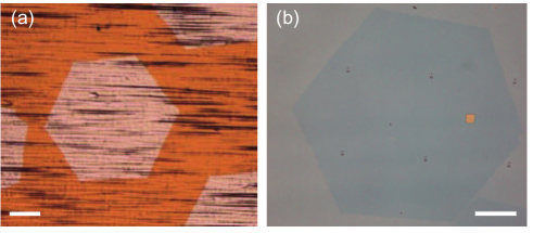
SLG single crystals are grown on 25m-thick Alfa Aesar, 99.8% purity Cu foil, Fig.1a. As for Ref.42, before growth the Cu foil is floated on the surface of a 30% hydrogen peroxide (H2O2) solution at 100∘C for 5min to oxidize the back-side. This treatment favours the growth of single crystals due to oxygen-enabled scavanging of carbon impurities trapped in the Cu top surface and bulk, which would otherwise act as nucleation sites during the growthBraeCM2016 . Growth is then performed in a Aixtron Black Magic Pro, 4-inch cold wall plasma enhanced-CVD (PECVD) system with a base pressure0.05mbar. The foil is initially placed in the furnace and heated to1065∘C in a Ar environment (200sccm) at 100∘C/min. Once the growth is reached, the Cu foil is annealed keeping constant in Ar (200sccm) for 30min. Carbon deposition is done in an Ar/H2 environment (250/26sccm) using 9sccm CH4, 0.1% diluted in Ar, for 45min. Samples are then cooled in 250sccm Ar to RT. The crystallinity of the as grown-SLG is confirmed via transmission electron microscopy (TEM)BraeCM2016 . Electron diffraction on multiple spots reveals the same crystal orientation across the hexagonal SLG domain with lateral sizeBraeCM2016 . SLG crystals are then transferred on Si+285nm SiO2 using a wet methodLiS2009 ; BaeNN2010 ; BonaMT2012 . A poly(methyl methacrylate) (PMMA) support layer is spin coated at the SLG surface, following which the samples are placed in a solution of ammonium persulfate (APS) and deionized (DI) water, whereby Cu is chemically etchedLiS2009 ; BaeNN2010 ; BonaMT2012 . The PMMA/SLG stack is then moved to a beaker with DI water to remove APS residuals and lifted with the target SiO2/Si substrate. After drying, PMMA is removed in acetone, leaving SLG on SiO2/Si, Fig.1b. We then encapsulate SLG in hBN. hBN bulk crystals are grown as for Ref.43. These are mechanically exfoliated on Si+285nm SiO2 to be used for SLG encapsulation. Flakes of lateral sizem are identified and selected by inspecting the SiO2/Si surface using a combination of bright and dark field optical microscopy, Raman spectroscopy and atomic force microscopy (AFM). For the top hBN we use flakes with thickness t2-300nm. For the bottom hBN, flakes with 10nm are chosen, as thinner ones do not screen roughness and charged impurities of the underlying SiO2DeanNN2010 ; PurdNC2018 .


The encapsulation of SLG in hBN typically results in blisters containing trapped adsorbates and contaminantsKretNL2014 , which must be avoided as they locally degrade transportKretNL2014 . Ref.46 showed how to remove contamination blisters by a hot pick-up technique. This uses above the glass transition, , of the polymer stamp during encapsulation, allowing the interfaces of two materials to be brought together in a directional, conformal mannerPizzNC2016 . We modified this approach by using polycarbonate (PC) stamps at C, achieving fast () removal of contaminants in fully-encapsulated hBN/SLG/hBN heterostructuresPurdNC2018 . This results in atomically-flat interfaces even on samples intentionally contaminated with polymers and solvents, achieving in all cases RT PurdNC2018 . As for Ref.15, here we use a transfer stamp consisting of a PC film on a polydimethylsiloxane (PDMS) block for mechanical support, placed on a glass slide attached to a micro-manipulator, enabling fine () spatial control in x, y and z. is set using a heated stage. The process is depicted in Fig.2. It begins by positioning the stamp above a hBN flake, then lowering it into contact, with the stage set to C. As the stamp is withdrawn, the hBN adheres to the PC surface, and is delaminated from SiO2, Fig.2b,c. The picked-up hBN is then positioned above the (wet transferred) SLG on SiO2 and brought into contact at C. We then wait5mins to promote adhesion between hBN and SLG, after which the stamp is lifted, picking up the SLG portion in contact with hBN, Fig.2d,e. The final step consists in bringing the top hBN/SLG into contact with the bottom hBN at C, with the stamp tilted to ensure that contact occurs first on one side, then conformally advancing across the substrate, Fig.2f. At C, withdrawing the stamp releases the PC onto the substrate, Fig.2g, then dissolved by placing the sample in chloroform, Fig.2h. Figs.3a,b are bright and dark field images of the final hBN/SLG/hBN stack. Scans by AFM, Fig.3c, reveal that some blisters are present. They tend to aggregate in specific areas, mostly along vertical lines, which we attribute to residual wrinkles from wet transfer.
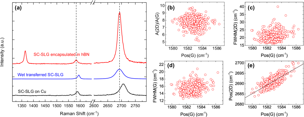
The SLG quality is monitored at each step of the fabrication process by Raman spectroscopy. Raman measurements are performed with a Renishaw InVia spectrometer equipped with a 100 objective, 2400l/mm grating at 514nm. The power on the sample is below1mW to avoid any heating and damage. Fig.4a plots representative spectra of a SC-SLG on Cu (black), after transfer on SiO2/Si (blue) and encapsulated in hBN (red). The SLG spectrum on Cu is shown after subtraction of the Cu photoluminescence (PL)LagaAPL2013 . This has a 2D peak with a single Lorentzian shape and a with full width at half maximum FWHM(2D)27cm-1, a signature of SLGFerrPRL2006 . The position of the G peak, Pos(G), is1588cm-1, with FWHM(G)14cm-1. The 2D peak position, Pos(2D) is2706cm-1, while the 2D to G peak intensity and area ratios, I(2D)/I(G) and A(2D)/A(G), are3 and5.5. No D peak is observed, indicating negligible defectsCancNL2011 ; FerrNN2013 . After wet transfer on SiO2/Si, the 2D peak retains its single-Lorentzian lineshape with FWHM(2D)30cm-1. The D peak is still negligible, indicating that no significant defects are induced by wet transfer. Pos(G) is1594cm-1, FWHM(G)11cm-1, Pos(2D)2692cm-1, I(2D)/I(G) and A(2D)/A(G) are2.5 and 6.8, indicating a doping200meVDasNN2008 ; BaskPRB2009 . After pick up and encapsulation, we perform a Raman mapping over an area20m m, using the same measurement conditions. A representative spectrum is shown in red in Fig.4a. This comprises both the SLG signatures and the hBN peak1364cm-1, with FWHM9.5cm-1, as expected for bulk hBNArenNL2006 ; ReicPRB2005 ; NemaPRB1979 . The hBN E2g peak is a combination of top and bottom hBN and may overlap a small D peak.
Fig.4b-e plot Raman data extracted from mapping: A(2D)/A(G), FWHM(2D), FWHM(G) and Pos(2D) as a function of Pos(G). Pos(G) depends on both dopingDasNN2008 ; BaskPRB2009 and strainMohiPRB2009 . This implies that local variations in strain and doping manifest as a spread in Pos(G) which, in our sample, varies from 1580 to 1586cm-1. The samples have narrow 2D peaks with mean FWHM(2D)203cm-1. Figs.4b-d plot A(2D)/A(G) and FWHM(G) as function of Pos(G), indicating small variations of both doping and strain within the SLG layer. The mean A(2D)/A(G) is7.80.7, while the mean FWHM(G) is15.41.2cm-1. The high A(2D)/A(G) is an indication of intrinsic samplesDasNN2008 , when combined with FWHM(G)cm-1, as well as Pos(G)cm-1 and Pos(2D)cm-1DasNN2008 .
The rate of change of Pos(2D) and Pos(G) with strain is ruled by the Grüneisen parameters ()MohiPRB2009 , which relate the relative change in the peak positions in response to strain(), i.e. , where is the frequency of Raman peaks at finite strain and the frequency at zero strainMohiPRB2009 . For biaxial strain the Grüneisen parameters for G and 2D peak are respectively and , resulting in Pos(2D)/Pos(G)MohiPRB2009 ; ZabeNL2012 ; ProcPRB2009 . In the case of uniaxial strain MohiPRB2009 , however extraction of is not straightforward, as uniaxial strain shifts the relative position of the SLG Dirac conesMohiPRB2009 ; ZabeNL2012 , which in turn affects the 2D peak, as this is involves by intervalley scatteringFerrNN2013 ; MohiPRB2009 . Ref.MohiPRB2009 experimentally derived an upper bound and theoretically calculated , consistent with experimentally reported Pos(2D)/Pos(G)MohiPRB2009 ; YoonPRL2011 ; LeeNC2012 . Biaxial strain can be differentiated from uniaxial from the absence of G and 2D peak splitting with increasing strainFerrNN2013 , however at low () strain the splitting cannot be resolvedMohiPRB2009 ; YoonPRL2011 . Fig.4e shows the correlation between Pos(2D) and Pos(G). A linear fit gives a slope Pos(2D)/Pos(G)2.07. The presence (or coexistence) of biaxial strain cannot be ruled out. For uniaxial(biaxial) strain, Pos(G) shifts by Pos(G)MohiPRB2009 ; YoonPRL2011 ; ZabeNL2012 . For intrinsic SLG (EmeV), the unstrained, undoped Pos(G) is1581.5cm-1FerrPRL2006 ; PiscPRL2004 . In Fig.4d the mean Pos(G) is 1582.8cm-1, which would lead to uniaxial(biaxial) strain 0.05%(0.02%)MohiPRB2009 ; YoonPRL2011 ; ZabeNL2012 . The scattering of A(2D)/A(G) within the mapped area indicates small (100meV) variation of doping.

We then process our samples into Hall-bars, in order to perform 4-terminal electrical transport. To form contacts, we follow Ref.13. After defining the shape of the desired Hall bar using a hard maskPurdNC2018 , patterned by e-beam lithography, we remove the unmasked part by reactive ion etching (RIE) using a plasma formed from a mix of tetrafluoromethane () and oxygen () (ratio 4:1) under a 20W forward radio frequency (RF) power. SLG is then contacted at its edgesWangS2013 by depositing metal leads via e-beam evaporation of 5/70nm Cr/Au.
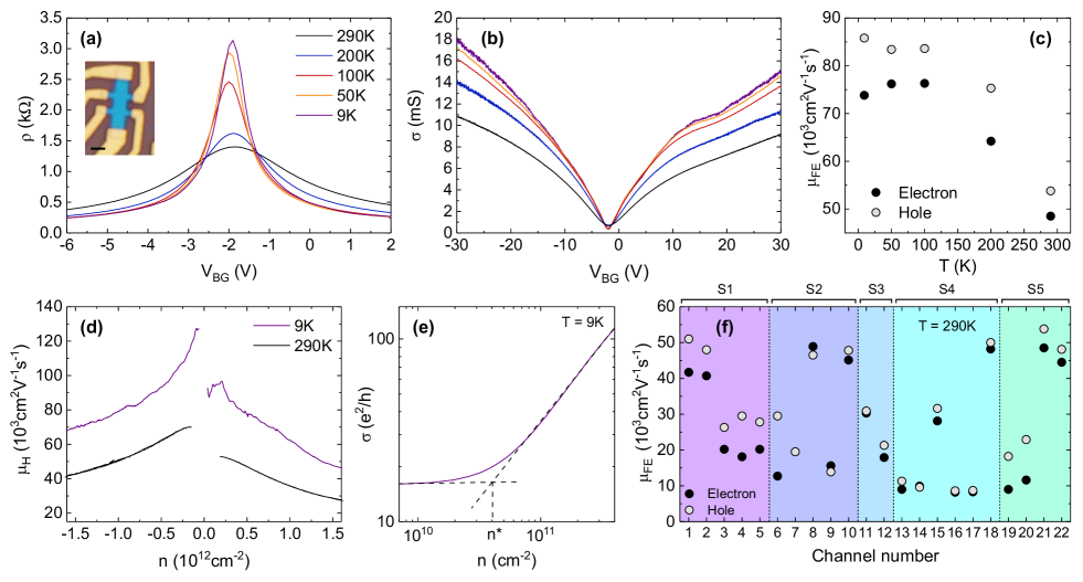
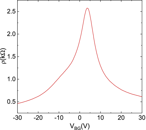
Fig.5a plots the resistivity of encapsulated CVD SLG as a function of back gate voltage . An optical image of one of the Hall bars is in the inset. The corresponding conductivity is shown in Fig.5b. We extract the field effect mobility by performing a linear fit to the conductivity close to the charge neutrality point (CNP)NovoS2004 , where is the gate capacitance per unit area. This is calculated as1.110-4F/m2, assuming a parallel plate capacitor where the bottom hBN is in series with the 285nm SiO2 layerPurdNC2018 . The bottom hBN thickness is15nm for the sample in Fig.5a. We assume a dielectric constant for hBN 3, considering that values between 2-4 are usually reportedKimACS2012 . Our is orders of magnitude smaller than the quantum capacitance of SLGXiaNN2009 , which is therefore neglected. This yields and for electrons and holes at 290K. as a function of in Fig.5c reaches for holes at 9K.
In order to extract as function of , we investigate transport in the presence of an out of plane magnetic field B (Hall effect)Sze2006 . To distinguish calculated from Hall effect from that estimated from the slope of the conductivity, we indicate the first as Sze2006 . Assuming a Drude model of conductivity Sze2006 , where is extracted by measuring the Hall voltage with B=0.5T. in Fig.5d reaches close to the CNP, while it is for up to. At 9K is.
Such values are consistent with those reported in CVD-grown SLG encapsulated in hBN using dry techniquesBansSA2015 ; BansNL2016 . E.g., Ref.39 measured in Hall bars made with CVD SLG encapsulated by dry transfer in hBN at 1.6K. The wet transfer method in Ref.PetrNL2012 resulted in up to at 1.6KPetrNL2012 , lower than here.
Fig.5a shows that our SLG is nearly intrinsic, since the resistivity peak occurs close to zero gate voltage, at , indicating moderate , in agreement with the Raman analysis. Furthermore, the resistivity peak is narrow, with FWHM1V at 9K. This places an upper bound on the disorder induced charge inhomogeneity, , with narrower peaks corresponding to lower disorderCoutPRX2014 ; BoloSSC2008 ; KretNL2014 . is typically associated with either suspendedCoutPRX2014 , or dry encapsulated samplesBansSA2015 ; PurdNC2018 . We extract for our sample as for Refs.10; 66, Fig.5e, and get, one order of magnitude higher than clean MC samplesPurdNC2018 .
In order to investigate the variation, we fabricate 22 Hall bars from 5 encapsulated SC-SLG. The distribution of at RT in Fig.5f ranges from a minimum up to. Bend resistance measurements as a function of are typically used to probe ballistic transport in SLGMayoNL2011 ; BansSA2015 ; WangS2013 ; PurdNC2018 , whereby current is injected around a bend while measuring the voltage. In SLG the carrier mean free path is related to conductivityHwanPRL2007 :
| (1) |
where is the Planck constant. can be extracted from Fig.5a. It varies from at 290K up to at 9K. For such we expect ballistic transportMayoNL2011 . We therefore fabricate a Hall cross with arm width to perform bend resistance measurements as a function of MayoNL2011 ; WangS2013 ; BansNL2016 .
An AFM scan of the Hall cross is in the inset of Fig.6a. A constant current is passed between contacts 1 and 2, and the voltage between contacts 3 and 4 measured, from which is extracted. In the diffusive regime, where , a positive is measured, related to the sheet resistance via the Van-der Pauw formulaVandPRR1958 : . Alternatively, if , carriers injected at contact 1 follow ballistic trajectories to contact 3, resulting in . as a function of is in Fig.6b. Below 100K, becomes negative for positive VBG, indicating . At the transition from the diffusive to ballistic and , from which may be estimated rearranging Eq.1 by substituting , to giveMayoNL2011 :
| (2) |
where is the carrier concentration at which . At 9K, occurs at , as shown by the arrow in Fig.6a, corresponding to , in agreement with the peak from Fig.5d. Further confirmation of ballistic transport is achieved by applying an out of plane B, which results in the bending of electrons from their straight-line trajectories, deflecting them away from contact 3, and switching from negative to positive, Fig.6b. Magneto-transport at B=1.8T and 9K, Fig.6c, shows resolved Landau levels, consistent with Refs.36; 39, proving the high electronic quality of our samples.
For all our samples at 9K, even in Hall bars with channel widths. This is supported by the fact that Hall crosses with width exhibit no negative bend resistance at any . Our maximum is lower than dry transferred samples, in which typically exceeds the sample dimensions at low WangS2013 ; BansNL2016 , resulting in edge scattering limited conductivity. Indeed, the highest reported in literature areWangS2013 ; BansNL2016 , over an order of magnitude larger than here. However, we note that is not a limiting factor at RT, where is limited by electron-phonon scatteringHwanPRB2008 ; ChenNN2008 ; ParkNL14 .
In order to investigate the effect of grain boundaries on , we study of Poly-SLG, CVD-grown, encapsulated in hBN by using the same approach. Due to the small domain size, multiple crystal orientation are present within the same Hall bar. Poly-SLG is grown on 35m Cu, following Ref.23. The substrate is annealed in 20sccm H2 up to 1000∘C for 30min. Then, 5 sccm of CH4 is added for the growth to take place for an additional 30 min. The sample is then cooled in vacuum (1.3 mbar) to RT and unloaded from the chamber. SLG is wet transferred onto Si+285nm SiO2 and then encapsulated in hBN, following the same procedure as above, but with =180∘C in the pick up step, as higher is required to pick Poly-SLG from SiO2.
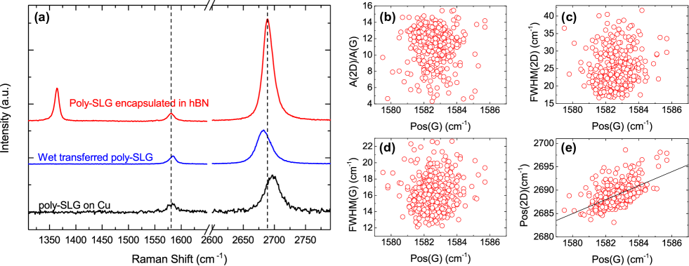
The Raman spectra at each stage of the transfer process are shown in Fig.7. Compared to SC-SLG, the Raman parameters are more scattered, e.g. the variation of A(2D)/A(G) and Pos(G) is twice that of SC-SLG, indicating inhomogeneous doping. The mean I(2D)/I(G) and A(2D)/A(G) ratio are indeed 7.22.1 and 11.14.1, respectively, which indicate a mean doping 100meV 100meV. Pos(G) in unstrained graphene with such low doping is1581.6cm-1LeeNC2012 . In our samples, however, the mean Pos(G) is 1582.6cm0.9cm-1, indicating the presence of uniaxial(biaxial) strain between 0.02%(0.05%) and 0.03%(0.09%) MohiPRB2009 ; YoonPRL2011 ; ZabeNL2012 . The slope of Pos(2D)/Pos(G) in Fig.7f is 1.5 lower than in SC-SLG, due to the inhomogeneous distribution of doping and strain in these samples.
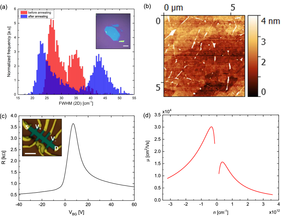
The resistivity as a function of is shown in Fig.8. By performing a linear fit to the conductivity close to CNP at , we get and for electrons and holes respectively at 290K. These values are one order of magnitude lower compared to SC-SLG, as expected from the presence of grain boundaries. The shoulder in the left hand side of the resistivity as a function of at suggests the presence of an additional CNP in the SLG channel, indicating inhomogeneous dopingBlakSSC2009 , in good agreement with the Raman analysis.
As in Poly-SLG is significantly lower that SC-SLG, we investigate the combined effect of thermal annealing and encapsulation in Poly-SLG. To do so, we first exfoliate hBN onto Si+285nm SiO2. Poly-SLG is then transferred to Si+285nm SiO2 using the polymer-based wet transfer detailed aboveLiS2009 ; BaeNN2010 ; BonaMT2012 . This results in SLG partially on SiO2 and partially on exfoliated hBN. The samples are then annealed at 600∘C in Ar/H2 (40/40sccm). Spatially-resolved Raman spectra are acquired before and after annealing, both on SLG on SiO2 and on hBN. The annealing sharpens FWHM(2D) from a mean27 to23 after annealing, Fig.9a. This suggests that annealing makes the sample more homogeneous in terms of doping/strain by aggregating adsorbates/contaminants in blisters as shown in Fig.9b. The annealed SLG is then encapsulated by depositing a second hBN using a polymer stamp following Ref.46. Samples are then shaped into Hall bars and contacted using Ni/Pd electrodes (30/40nm). Fig.9c plots the resistance as function of gate. Fig.9d shows in annealed and encapsulated Poly-SLG, indicating a peak , showing that annealing improves by a factor5. We note that this is amongst the highest RT claimed for Poly-SLG to date.
III Conclusions
We reported high mobility in CVD grown, single crystal SLG placed on Si+SiO2 using wet transfer and subsequently encapsulated in hBN. By cleaning interfaces between SLG and hBN atC, we achieved mobilities up to up at RT and at 9K, comparable to values achieved via dry transfer. The samples show ballistic transport over600nm at 9K. This confirms that encapsulation in hBN and interface cleaning enable high mobility even after conventional polymer-based wet transfer techniques. We also investigated the combined effect of annealing and encapsulation in polycrystalline SLG, achieving RT mobilities up to. Our results show that a scalable process such as wet-transfer can be used for the assembly of high-performance devices where high mobility () is essential.
IV Acknowledgements
We acknowledge funding from the EU Graphene Flagship, ERC Grant Hetero2D, EPSRC Grants EP/K016636/1, EP/K01711X/1, EP/K017144/1, EP/N010345/1, and EP/L016087/1, Wolfson College Cambridge, the Elemental Strategy Initiative conducted by MEXT and JSPS KAKENHI Grant JP15K21722.
References
- (1) S. M. Sze and K. K. Ng, Physics of semiconductor devices, (John Wiley & Sons, 2006).
- (2) J. H. Chen, C. Jang, S. D. Xiao, M. Ishigami and M. S. Fuhrer, Nat. Nanotechnol. 3, 206 (2008).
- (3) C. Park, N. Bonini, T. Sohier, G. Samsonidze, B. Kozinsky, M. Calandra, F. Mauri and N. Marzari, Nano Lett. 14, 1113 (2014).
- (4) M. Romagnoli, V. Sorianello, M. Midrio, F.H.L. Koppens, C. Huyghebaert, D. Neumaier, P. Galli, W. Templ, A. D’Errico and A.C. Ferrari, Nat. Rev. Mater., 3, 392-414, (2018).
- (5) Y. M. Lin, C. Dimitrakopoulos, K. A. Jenkins, D. B. Farmer, H. Y. Chiu, A. Grill and P. Avouris, Science 327, 662 (2010).
- (6) F. H. L. Koppens, T. Mueller, P. Avouris, A. C. Ferrari, M. S. Vitiello and M. Polini, Nat. Nanotechnol. 9, 780 (2014).
- (7) L. Vicarelli, M.S. Vitiello, D. Coquillat, A. Lombardo, A.C. Ferrari, W. Knap, M. Polini, V. Pellegrini and A. Tredicucci, Nat. Mater. 11 865 (2012).
- (8) V. Sorianello, M. Midrio, G. Contestabile, I. Asselberghs, J. Van Campenhout, C. Huyghebaert, I. Goykhman, A. K. Ott, A. C. Ferrari and M. Romagnoli, Nat. Photonics 12, 40 (2018).
- (9) K. I. Bolotin, K. J. Sikes, Z. Jiang, M. Klima, G. Fudenberg, J. Hone, P. Kim and H. L. Stormer, Solid State Commun. 146, 351 (2008).
- (10) X. Du, I. Skachko, A. Barker and E. Y. Andrei, Nat. Nanotechnol. 3, 491 (2008).
- (11) K. I. Bolotin, F. Ghahari, M. D. Shulman, H. L. Stormer and P. Kim, Nature 462, 196 (2009).
- (12) A. S. Mayorov, D. C. Elias, I. S. Mukhin, S. V. Morozov, L. A. Ponomarenko, K. S. Novoselov, A. K. Geim and R. V. Gorbachev, Nano Lett. 12, 4629 (2012)
- (13) L. Wang, I. Meric, P. Y. Huang, Q. Gao, Y. Gao, H. Tran, T. Taniguchi, K. Watanabe, L. M. Campos, D. A. Muller, J. Guo, P. Kim, J. Hone, K. L. Shepard and C. R. Dean, Science 342, 614 (2013).
- (14) A. S. Mayorov, R. V. Gorbachev, S. V. Morozov, L. Britnell, R. Jalil, L. A. Ponomarenko, P. Blake, K. S. Novoselov, K. Watanabe, T. Taniguchi and A. K. Geim, Nano Lett. 11, 2396 (2011).
- (15) D. G. Purdie, N. M. Pugno, T. Taniguchi, K. Watanabe, A. C. Ferrari and A. Lombardo, Nat. Commun. 9, 5387 (2018).
- (16) B. R. Bennett, R. Magno, J. B. Boos, W. Kruppa and M. G. Ancona, Solid State Electron. 49, 1875 (2005).
- (17) J. M. S. Orr, A. M. Gilbertson, M. Fearn, O. W. Croad, C. J. Storey, L. Buckle, M. T. Emeny, P. D. Buckle and T. Ashley, Phys. Rev. B 77, 165334 (2008).
- (18) T. Kobayashi, M. Bando, N. Kimura, K. Shimizu, K. Kadono, N. Umezu, K. Miyahara, S. Hayazaki, S. Nagai, Y. Mizuguchi, Y. Murakami and D. Hobara, Appl. Phys. Lett. 102, (2013).
- (19) G. A. Lopez and E. J. Mittemeijer, Scripta Mater. 51, 1 (2004).
- (20) X. Li, Y. Zhu, W. Cai, M. Borysiak, B. Han, D. Chen, R. D. Piner, L. Colombo and R. S. Ruoff, Nano Lett. 9, 4359 (2009).
- (21) C. Mattevi, H. Kim and M. Chhowalla, J. Mater. Chem. 21, 3324 (2011).
- (22) S. Bae, H. Kim, Y. Lee, X. F. Xu, J. S. Park, Y. Zheng, J. Balakrishnan, T. Lei, H. R. Kim, Y. I. Song, Y. J. Kim, K. S. Kim, B. Ozyilmaz, J. H. Ahn, B. H. Hong and S. Iijima, Nat. Nanotechnol. 5, 574 (2010).
- (23) X. S. Li, W. W. Cai, J. H. An, S. Kim, J. Nah, D. X. Yang, R. Piner, A. Velamakanni, I. Jung, E. Tutuc, S. K. Banerjee, L. Colombo and R. S. Ruoff, Science 324, 1312 (2009).
- (24) Q. Yu, L. A. Jauregui, W. Wu, R. Colby, J. Tian, Z. Su, H. Cao, Z. Liu, D. Pandey, D. Wei, T. F. Chung, P. Peng, N. P. Guisinger, E. A. Stach, J. Bao, S.-S. Pei and Y. P. Chen, Nat. Mater. 10, 443 (2011).
- (25) X. S. Li, C. W. Magnuson, A. Venugopal, R. M. Tromp, J. B. Hannon, E. M. Vogel, L. Colombo and R. S. Ruoff, J. Am. Chem. Soc. 133, 2816 (2011).
- (26) V. Miseikis, F. Bianco, J. David, M. Gemmi, V. Pellegrini, M. Romagnoli and C. Coletti, 2D Mater. 4, 021004 (2017).
- (27) L. Gao, W. Ren, H. Xu, L. Jin, Z. Wang, T. Ma, L.-P. Ma, Z. Zhang, Q. Fu, L.-M. Peng, X. Bao and H.-M. Cheng, Nat. Commun. 3, 699 (2012).
- (28) I. Vlassiouk, M. Regmi, P. Fulvio, S. Dai, P. Datskos, G. Eres and S. Smirnov, ACS Nano 5, 6069 (2011).
- (29) S. Bhaviripudi, X. Jia, M. S. Dresselhaus and J. Kong, Nano Lett. 10, 4128 (2010).
- (30) Z. Yan, J. Lin, Z. Peng, Z. Sun, Y. Zhu, L. Li, C. Xiang, E. L. Samuel, C. Kittrell and J. M. Tour, ACS Nano 6, 9110 (2012).
- (31) H. Wang, G. Wang, P. Bao, S. Yang, W. Zhu, X. Xie and W.-J. Zhang, JJ. Am. Chem. Soc. 134, 3627 (2012).
- (32) F. Bonaccorso, A. Lombardo, T. Hasan, Z. P. Sun, L. Colombo and A. C. Ferrari, Mater. Today 15, 564 (2012).
- (33) Q. K. Yu, J. Lian, S. Siriponglert, H. Li, Y. P. Chen, and S. S. Pei, Appl. Phys. Lett. 93 (2008).
- (34) Y. Wang, Y. Zheng, X. F. Xu, E. Dubuisson, Q. L. Bao, J. Lu and K. P. Loh, ACS Nano 5, 9927 (2011).
- (35) W. Gannett, W. Regan, K. Watanabe, T. Taniguchi, M. F. Crommie and A. Zettl, Appl. Phys. Lett. 98, 242105 (2011).
- (36) N. Petrone, C. R. Dean, I. Meric, A. M. van der Zande, P. Y. Huang, L. Wang, D. Muller, K. L. Shepard and J. Hone, Nano Lett. 12, 2751 (2012).
- (37) V. E. Calado, S. E. Zhu, S. Goswami, Q. Xu, K. Watanabe, T. Taniguchi, G. C. A. M. Janssen and L. M. K. Vandersypen, Appl. Phys. Lett. 104, 023103 (2014).
- (38) R. Wang, P. R. Whelan, P. Braeuninger-Weimer, S. Tappertzhofen, J. A. Alexander-Webber, Z. A. Van Veldhoven, P. R. Kidambi, B. S. Jessen, T. Booth, P. Bøggild and S. Hofmann, ACS Appl. Mater. Interfaces 8, 33072 (2016).
- (39) L. Banszerus, M. Schmitz, S. Engels, J. Dauber, M. Oellers, F. Haupt, K. Watanabe, T. Taniguchi, B. Beschoten and C. Stampfer, Sci. Adv. 1, e150022 (2015).
- (40) M. Droegeler, L. Banszerus, F. Volmer, T. Taniguchi, K. Watanabe, B. Beschoten and C. Stampfer, Appl. Phys. Lett. 111, 152402 (2017).
- (41) S. Chen, L. Brown, M. Levendorf, W. Cai, S.-Y. Ju, J. Edgeworth, X. Li, C. W. Magnuson, A. Velamakanni, R. D. Piner, J. Kang, J. Park and R. S. Ruoff, ACS Nano 5, 1321 (2011).
- (42) P. Braeuninger-Weimer, B. Brennan, A. J. Pollard and S. Hofmann, Chem. Mater. 28, 8905 (2016).
- (43) T. Taniguchi and K. Watanabe, J. Cryst. Growth. 303, 525 (2007).
- (44) C. R. Dean, A. F. Young, I. Meric, C. Lee, L. Wang, S. Sorgenfrei, K. Watanabe, T. Taniguchi, P. Kim, K. L. Shepard and J. Hone, Nat. Nanotechnol. 5, 722 (2010).
- (45) A. V. Kretinin, Y. Cao, J. S. Tu, G. L. Yu, R. Jalil, K. S. Novoselov, S. J. Haigh, A. Gholinia, A. Mishchenko, M. Lozada, T. Georgiou, C. R. Woods, F. Withers, P. Blake, G. Eda, A. Wirsig, C. Hucho, K. Watanabe, T. Taniguchi, A. K. Geim et al., Nano Lett. 14, 3270 (2014).
- (46) F. Pizzocchero, L. Gammelgaard, B. S. Jessen, J. M. Caridad, L. Wang, J. Hone, P. Boggild and T. J. Booth, Nat. Commun. 7, 11894 (2016).
- (47) A. A. Lagatsky, Z. Sun, T. S. Kulmala, R. S. Sundaram, S. Milana, F. Torrisi, O. L. Antipov, Y. Lee, J. H. Ahn, C. T. A. Brown, W. Sibbett and A. C. Ferrari, Appl. Phys. Lett. 102, 013113 (2013).
- (48) A. C. Ferrari, J. C. Meyer, V. Scardaci, C. Casiraghi, M. Lazzeri, F. Mauri, S. Piscanec, D. Jiang, K. S. Novoselov, S. Roth and A. K. Geim, Phys. Rev. Lett. 97, 187401 (2006).
- (49) A. C. Ferrari and D. M. Basko, Nat. Nanotechnol. 8, 235 (2013).
- (50) L. G. Cancado, A. Jorio, E. H. Ferreira, F. Stavale, C. A. Achete, R. B. Capaz, M. V. Moutinho, A. Lombardo, T. S. Kulmala and A. C. Ferrari, Nano Lett. 11, 3190 (2011).
- (51) A. Das, S. Pisana, B. Chakraborty, S. Piscanec, S. K. Saha, U. V. Waghmare, K. S. Novoselov, H. R. Krishnamurthy, A. K. Geim, A. C. Ferrari and A. K. Sood, Nat. Nanotechnol. 3, 210 (2008).
- (52) D. M. Basko, S. Piscanec and A. C. Ferrari, Phys. Rev. B 80, 165413 (2009).
- (53) R. Arenal, A. C. Ferrari, S. Reich, L. Wirtz, J. Y. Mevellec, S. Lefrant, A. Rubio and A. Loiseau, Nano Lett. 6, 1812 (2006).
- (54) S. Reich, A. C. Ferrari, R. Arenal, A. Loiseau, I. Bello and J. Robertson, Phys. Rev. B 71, (2005).
- (55) R. J. Nemanich and S. A. Solin, Phys. Rev. B 20, 392 (1979).
- (56) T. M. G. Mohiuddin, A. Lombardo, R. R. Nair, A. Bonetti, G. Savini, R. Jalil, N. Bonini, D. M. Basko, C. Galiotis, N. Marzari, K. S. Novoselov, A. K. Geim and A. C. Ferrari, Phys. Rev. B 79, 205433 (2009).
- (57) J. E. Proctor, E. Gregoryanz, K. S. Novoselov, M. Lotya, J. N. Coleman and M. P. Halsall, Phys. Rev. B 80, 073408 (2009).
- (58) J. Zabel, R. R. Nair, A. Ott, T. Georgiou, A. K. Geim, K. S. Novoselov and C. Casiraghi, Nano Lett. 12, 617 (2012).
- (59) D. Yoon, Y.W. Son and H. Cheong, Phys. Rev. Lett. 106, 155502 (2011).
- (60) J. E. Lee, G. Ahn, J. Shim, Y. S. Lee and S. Ryu, Nat. Commun. 3, 1024 (2012).
- (61) S. Piscanec, M Lazzeri, A. C. Ferrari and J. Robertson, Phys. Rev. Lett. 93, 185503 (2004).
- (62) K. S. Novoselov, A. K. Geim, S. V. Morozov, D. Jiang, Y. Zhang, S. V. Dubonos, I. V. Grigorieva and A. A. Firsov, Science 306, 666 (2004).
- (63) K. K. Kim, A. Hsu, X. Jia, S. M. Kim, Y. Shi, M. Dresselhaus, T. Palacios and J. Kong, ACS Nano 6, 8583 (2012).
- (64) J. Xia, F. Chen, J. Li and N. Tao, Nat. Nanotechnol. 4, 505 (2009).
- (65) L. Banszerus, M. Schmitz, S. Engels, M. Goldsche, K. Watanabe, T. Taniguchi, B. Beschoten and C. Stampfer, Nano Lett. 16, 1387 (2016).
- (66) N. J. G. Couto, D. Costanzo, S. Engels, D. K. Ki, K. Watanabe, T. Taniguchi, C. Stampfer, F. Guinea and A. F. Morpurgo, Phys. Rev. X 4, 041019 (2014).
- (67) E. H. Hwang, S. Adam and S. Das Sarma, Phys. Rev. Lett. 98, (2007).
- (68) L. J. Van der Pauw, Philips Res. Rep. 13, 1 (1958).
- (69) E. H. Hwang and S. Das Sarma, Phys. Rev. B 77, 115449 (2008).
- (70) P. Blake, R. Yang, S. V. Morozov, F. Schedin, L. A. Ponomarenko, A. A. Zhukov, R. R. Nair, I. V. Grigorieva, K. S. Novoselov and A. K. Geim, Solid State Commun. 149, 1068 (2009).