Optically coherent nitrogen-vacancy centers in -thin etched diamond membranes
Abstract
Diamond membrane devices containing optically coherent nitrogen-vacancy (NV) centers are key to enable novel cryogenic experiments such as optical ground-state cooling of hybrid spin-mechanical systems and efficient entanglement distribution in quantum networks. Here, we report on the fabrication of a (3.4 0.2) thin, smooth (surface roughness rq 0.4 nm over an area of 20 by 30 ) diamond membrane containing individually resolvable, narrow linewidth ( 100 MHz) NV centers. We fabricate this sample via a combination of high energy electron irradiation, high temperature annealing, and an optimized etching sequence found via a systematic study of the diamond surface evolution on the microscopic level in different etch chemistries. While our particular device dimensions are optimized for cavity-enhanced entanglement generation between distant NV centers in open, tuneable micro-cavities, our results have implications for a broad range of quantum experiments that require the combination of narrow optical transitions and -scale device geometry.
The negative nitrogen-vacancy (NV) center is a point defect center in diamond [1, 2] that is used in a wide range of experiments, including quantum sensing [3, 4, 5, 6, 7], quantum computation algorithms [8, 9], and quantum communication [10, 11, 12]. In addition to second-long spin coherence times [13] and spin-conserving optical transitions [14], NV centers feature coupling to nearby nuclear spins that can act as memory quantum bits [15, 16, 11]. Many NV-based experiments require a combination of good optical and spin properties in nano-fabricated structures; these experiments include Purcell enhancement of the optical zero-phonon line (ZPL) transitions in a diamond micro-cavity [17, 18, 19, 20, 21, 22, 23, 24, 25, 26, 27, 28, 29, 30] for entanglement generation speed-up, optical ground state cooling of a hybrid NV-cantilever spin-mechanical system [31, 32, 33, 34, 35, 36], and resonant optical readout of NV centers in sensing applications [14]. While good spin coherence has been demonstrated for surface-proximal NVs (depth of 50 nm) [37, 38, 39], the incorporation of optically coherent NV centers in -scale devices remains an outstanding challenge.
The optically excited state of the NV center is sensitive to electric fields and crystal strain [40]. Therefore, high-frequency electric field noise can lead to dephasing in the excited state, while on longer timescales the transitions can be effectively widened by slow spectral diffusion originating from a changing charge state distribution in the environment [41, 42]. Although the latter effect can be mitigated by actively tracking the transition frequencies and adding feedback [10], it comes at the cost of reduced experimental repetition rates. Dephasing poses a more fundamental challenge: in hybrid-mechanical systems, effective optical ground state cooling requires operation in the sideband resolved regime [31, 34]. Dephasing also determines the resolvable magnetic field changes in sensing experiments, and limits the two-photon quantum interference contrast that translates into state fidelity for entanglement protocols [43, 44]. For all discussed applications of NV centers in membranes, spectral diffusion widths MHz and dephasing widths MHz are in practice desired. However, reported spectral diffusion widths in thin ( 1 ) nanofabricated structures are 1 GHz [30] for NV centers formed via nitrogen implantation [45]. Improvements in fabrication and preparation methods are therefore necessary to produce devices with linewidths sufficiently narrow for the experiments discussed above.
For our desired application of embedding a diamond membrane in an open, tuneable Fabry-Perot microcavity to increase entanglement generation rates between distant NV centers [28, 29, 46, 30, 47], we target a final membrane thickness of 4 . This choice is a compromise between low cavity mode volume needed for high Purcell enhancement and sufficient thickness to avoid frequent breaking of membranes during sample handling, whilst being able to embed NVs as deep in the diamond lattice as possible to avoid surface-induced noise. We furthermore require smooth samples (r 0.3 nm over the 4 2 large area of the cavity beam waist) to limit losses due to scattering at the diamond-air interface [46, 48].
Here, we report on a full fabrication procedure that combines high energy electron irradiation, high temperature annealing, and an optimized etching sequence, to yield a diamond device that meets all the above requirements. We verify the desired NV center optical properties using an extensive study on linewidths following different etching steps.
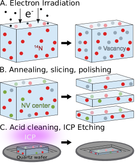
We start from ultrapure, CVD grown diamond that contains only a few NV centers [49], and thus requires their density to be increased. NV centers created from implanted nitrogen atoms were recently found to predominately feature broad optical lines, likely due to associated diamond lattice damage [50]. Instead, we use high energy electron irradiation to create vacancies throughout the whole diamond that can form NV centers with native nitrogen [51] (see Fig. 1 (A)). After tri-acid cleaning, a high temperature and high vacuum annealing sequence — consisting of three temperature steps — ensures the recombination of vacancies with naturally occurring nitrogen in the diamond to form NV centers, and anneals out vacancy chains [52, 53] (see Fig. 1 (B)). The resulting density of NV centers thus depends on the nitrogen distribution resulting from diamond growth, and the number of vacancies created during electron irradiation [49]. The diamonds are subsequently sliced and polished into three membranes of 50 thickness each. This value is a trade-off between ease of handling of the membranes in further processing steps, and the amount of material that needs to be removed in a subsequent reactive ion etching (RIE) step using an Inductively Coupled Plasma (ICP) (see Fig. 1 (C)).
To find an etch recipe that leads to smooth, thin diamonds, we investigate the effect of different etch chemistries on the diamond surface roughness on the microscopic level. It is advantageous to employ an oxygen-based ICP-RIE, due to reported high diamond etch rates ( 200 nmmin [54]), and an oxygen-rich surface termination of the diamond, which is beneficial for the charge state stability of the NV- center [55]. However, it has been speculated that particles, e.g. those introduced during the diamond polishing process, can lead to hole formation during etching with O2 [56, 57].
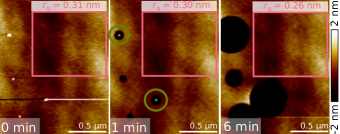
By overlaying Atomic Force Microscope (AFM) surface images of identical diamond areas before and after O2 etching, we find that each of the observed circular pits originates from a particle that was initially present at that location. Fig. 2 shows the evolution of one such area before etching, and after 1 and 6 minutes of etching with O2 [49]. The data demonstrates that the underlying mechanism of hole formation is micro-masking: the particle etch rate is lower than that of the bulk diamond surface. This leads to the formation of diamond nanopillars on the surface that deflect the impinging plasma, which enhances the etch rate locally and thus creates a hole around the pillar [54] (see the green encircled areas in Fig. 2 after 1 minute of etching). Due to an isotropic etch component, the pillars are eventually etched away, leaving behind a hole. These holes then remain, and widen as the etching continues. Importantly, we also find that the membrane surface roughness can be maintained during O2 etching if particle-induced holes are excluded (see the pink rectangles in Fig. 2). Even after extended O2 etches, one thus expects to maintain the intitial diamond surface roughness if particles can be effectively removed before this step.
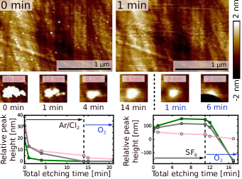
To reduce the number of particles on the diamond surface to levels lower than after acid cleaning alone [49], common strategies are to etch under Ar/Cl2 [58] or SF6 [59]. However, Ar/Cl2 etching induces Cl contamination on the diamond surface [60], which is suspected to have a detrimental influence on the optical and spin properties of NV centers. Therefore, Ar/Cl2 is often combined with O2 etching [7, 53, 61, 62, 30, 59]. Fig. 3 confirms that Ar/Cl2 is indeed highly effective in removing particles, and that it can be followed by O2 etching without forming holes on the surface. By comparing the evolution of the relative peak height of particles w.r.t. the mean of the surrounding diamond surface (see Fig. 3, bottom graphs), we find that Ar/Cl2 is more efficient in removing particles from the diamond surface than SF6 [49]: while Ar/Cl2 removes small particles within the first minute of etching and continues to reduce the relative peak height of large debris for longer etching times, it takes longer for small particles to be removed in SF6, and the relative peak height of some larger remaining structures increases during etching in this chemistry, leading to the formation of holes.
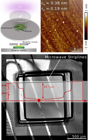
Using the above etch recipe, we fabricate a sample following the steps in Fig. 1. For microwave delivery and repeated identification of the measurement area, the sample is bonded via Van der Waals forces to a super-polished mirror patterned with golden striplines and unique position markers before etching [63]. We have observed that the exposure of mirror material to the plasma leads to severe micromasking on the diamond as etched mirror material is re-deposited on the diamond surface. This results in the formation of holes on the diamond following the same mechanism as discussed above. To mitigate this effect, we use a fused quartz mask for partial exposure of the diamond [62] (see Fig. 4 (Top left)). We thin the sample in three etching steps, each consisting of an Ar/Cl2 pre-etch, followed by a single O2 step, for a total etch duration of 86 minutes of Ar/Cl2 and 206 minutes of O2 etching. Fig. 4 (Bottom) shows a confocal microscope image and stylus profilometer height trace of the bonded membrane after the full etching sequence. The geometry of the mask restricts the solid angle of incidence and leads to a position-dependent etch rate. Therefore, the sample height profile shows a curvature in the exposed region, with a thinnest membrane thickness of (3.4 0.2) . The red dot indicates the (3.8 0.2) thick area within which the AFM image in Fig. 4 (Top right) was taken after the full etch. This image confirms a smooth diamond surface ( = 0.38 nm over a 20 by 30 area) even after this prolonged etch sequence.
We characterize the optical properties of NV centers in between etch steps in a confocal microscopy setup 10 K by using a largely automatized measurement sequence to determine their linewidths via photo-luminescence excitation (PLE) scans of the ZPL transitions [49]. After roughly localizing an NV transition in frequency space, we scan a tuneable laser around this frequency, while detecting photons emitted from the NV in the phonon side band (PSB). We repeatedly apply a sequence of a short green laser pulse (to ensure spin and charge state initialization), followed by a red frequency sweep through the expected transition frequency (to map out the specific ZPL transition under dephasing). We do this while constantly applying microwaves to avoid pumping in an optically dark spin state. By performing many scans of this kind, we probe both the effects of spectral diffusion (via a fit to the averaged counts of all scans), as well as the average dephasing width (by fitting each scan individually, and calculating the weighted mean for all fitted linewidths).
Fig. 5 shows the results of spectral diffusion and dephasing widths as a function of distance from the mirror interface for a total of 155 NV center transitions, stemming from 110 distinguishable NV centers. This data has been acquired at four different steps during membrane thinning and thus membrane thicknesses tm in the measurement region. While we are not able to track identical NV centers throughout the different etch steps, we make sure to look at the same 20 by 20 area of diamond for all measurements, apart from the data for the thinnest membrane, for which we additionally included a second region 200 from the main measurement area for increased statistics.
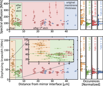
The data shows the potential of electron irradiation as a reliable way of introducing coherent NV centers throughout the membrane: for the unetched case, we find an average dephasing width of (39 6) MHz, and an average spectral diffusion width of (122 44) MHz. We suspect that laser-power induced linewidth broadening prevents us from resolving lifetime limited values for the dephasing linewidths [49]. Importantly, for membranes etched down to tm = (37.7 0.2) and to tm = (10.1 0.2) , we observe that all linewidth averages overlap within statistical uncertainties.
We find roughly two times broader linewidths when characterizing NVs at the final membrane thickness of tm = (3.8 0.2) in the measurement region; the spectral diffusion width averages to (189 117) MHz, while the dephasing width averages to (86 33) MHz. Yet, even for this thickness, we find that 22 out of 37 measured NV centers fulfill our pre-set criteria of dephasing linewidth 100 MHz and spectral diffusion linewidth 250 MHz.
The NV ZPL transitions shift with crystal strain: while axial strain results in an overall resonance frequency shift, transverse strain splits the and optical transitions [1]. To determine whether strain in the diamond influences the observed linewidth broadening, we extract the transverse and axial strain from a subset of NV centers via a reconstruction of the NV center Hamiltonian [49]. Although the average axial and transverse strain increase with decreasing NV distance from the mirror interface, the data does not show a dependency of the measured spectral diffusion and dephasing linewidths on strain [49], suggesting that there is no direct causal relation between the two. Possible causes of increased strain found for NVs after the last etching step include a stressed layer that remains after the membrane polishing process [64, 65, 66], effects due to bonding of the diamond to the mirror (including stress resulting from the difference in thermal expansion coefficients for the diamond and mirror), and lattice-damage induced by reflection of ions from the diamond-mirror interface. Future systematic studies beyond the current work are required to pinpoint the origin unambiguously.
In conclusion, we have demonstrated the fabrication of a diamond sample with a high density of NV centers, introduced through electron irradiation and subsequent high temperature annealing. The surface roughness (r 0.4 nm for a 20 by 30 area), thickness ( 4 ) and NV linewidths ( 100 MHz) of this sample allow for enhanced entanglement generation rates via the Purcell effect in an open, tuneable microcavity setup. Given these sample properties and vibration levels of 0.1 nm rms under pulse-tube operation [47], we expect an emission of ZPL photons coupled into the fiber mode of 35 [48], which translates into an entanglement rate enhancement of two orders of magnitude. This would allow one to form a quantum repeater beating direct transmission [67, 68, 69], signaling the surpassing of a fundamental milestone on the route to building a quantum network.
References
- Doherty et al. [2013] M. W. Doherty, N. B. Manson, P. Delaney, F. Jelezko, J. Wrachtrup, and L. C. L. Hollenberg, Physics Reports 528, 1 (2013).
- Atatüre et al. [2018] M. Atatüre, D. Englund, N. Vamivakas, S. Y. Lee, and J. Wrachtrup, Nature Reviews Materials 3, 38 (2018).
- Degen [2008] C. L. Degen, Applied Physics Letters 92, 243111 (2008).
- Maze et al. [2008] J. R. Maze, P. L. Stanwix, J. S. Hodges, S. Hong, J. M. Taylor, P. Cappellaro, L. Jiang, M. V. Dutt, E. Togan, A. S. Zibrov, A. Yacoby, R. L. Walsworth, and M. D. Lukin, Nature 455, 644 (2008).
- Balasubramanian et al. [2008] G. Balasubramanian, I. Y. Chan, R. Kolesov, M. Al-Hmoud, J. Tisler, C. Shin, C. Kim, A. Wojcik, P. R. Hemmer, A. Krueger, T. Hanke, A. Leitenstorfer, R. Bratschitsch, F. Jelezko, and J. Wrachtrup, Nature 455, 648 (2008).
- Grinolds et al. [2011] M. S. Grinolds, P. Maletinsky, S. Hong, M. D. Lukin, R. L. Walsworth, and A. Yacoby, Nature Physics 7, 687 (2011).
- Maletinsky et al. [2012] P. Maletinsky, S. Hong, M. S. Grinolds, B. Hausmann, M. D. Lukin, R. L. Walsworth, M. Loncar, and A. Yacoby, Nature Nanotechnology 7, 320 (2012).
- Waldherr et al. [2014] G. Waldherr, Y. Wang, S. Zaiser, M. Jamali, T. Schulte-Herbrüggen, H. Abe, T. Ohshima, J. Isoya, J. F. Du, P. Neumann, and J. Wrachtrup, Nature 506, 204 (2014).
- Cramer et al. [2016] J. Cramer, N. Kalb, M. A. Rol, B. Hensen, M. S. Blok, M. Markham, D. J. Twitchen, R. Hanson, and T. H. Taminiau, Nature Communications 7, 1 (2016).
- Hensen et al. [2015] B. Hensen, H. Bernien, A. E. Dréau, A. Reiserer, N. Kalb, M. S. Blok, J. Ruitenberg, R. F. Vermeulen, R. N. Schouten, C. Abellán, W. Amaya, V. Pruneri, M. W. Mitchell, M. Markham, D. J. Twitchen, D. Elkouss, S. Wehner, T. H. Taminiau, and R. Hanson, Nature 526, 682 (2015).
- Kalb et al. [2017] N. Kalb, A. A. Reiserer, P. C. Humphreys, J. J. Bakermans, S. J. Kamerling, N. H. Nickerson, S. C. Benjamin, D. J. Twitchen, M. Markham, and R. Hanson, Science 356, 928 (2017).
- Humphreys et al. [2018] P. C. Humphreys, N. Kalb, J. P. Morits, R. N. Schouten, R. F. Vermeulen, D. J. Twitchen, M. Markham, and R. Hanson, Nature 558, 268 (2018).
- Abobeih et al. [2018] M. H. Abobeih, J. Cramer, M. A. Bakker, N. Kalb, M. Markham, D. J. Twitchen, and T. H. Taminiau, Nature Communications 9, 1 (2018).
- Robledo et al. [2011] L. Robledo, L. Childress, H. Bernien, B. Hensen, P. F. A. Alkemade, and R. Hanson, Nature 477, 574 (2011).
- Maurer et al. [2012] P. C. Maurer, G. Kucsko, C. Latta, L. Jiang, N. Y. Yao, S. D. Bennett, F. Pastawski, D. Hunger, N. Chisholm, M. Markham, D. J. Twitchen, J. I. Cirac, and M. D. Lukin, Science 336, 1283 (2012).
- Taminiau et al. [2014] T. H. Taminiau, J. Cramer, T. Van Der Sar, V. V. Dobrovitski, and R. Hanson, Nature Nanotechnology 9, 171 (2014).
- Englund et al. [2010] D. Englund, B. Shields, K. Rivoire, F. Hatami, J. Vučković, H. Park, and M. D. Lukin, Nano Letters 10, 3922 (2010).
- Wolters et al. [2010] J. Wolters, A. W. Schell, G. Kewes, N. Nüsse, M. Schoengen, H. Döscher, T. Hannappel, B. Löchel, M. Barth, and O. Benson, Applied Physics Letters 97 (2010), 10.1063/1.3499300.
- Van Der Sar et al. [2011] T. Van Der Sar, J. Hagemeier, W. Pfaff, E. C. Heeres, S. M. Thon, H. Kim, P. M. Petroff, T. H. Oosterkamp, D. Bouwmeester, and R. Hanson, Applied Physics Letters 98, 1 (2011).
- Faraon et al. [2012] A. Faraon, C. Santori, Z. Huang, V. M. Acosta, and R. G. Beausoleil, Physical Review Letters 109, 2 (2012).
- Hausmann et al. [2013] B. J. Hausmann, B. J. Shields, Q. Quan, Y. Chu, N. P. De Leon, R. Evans, M. J. Burek, A. S. Zibrov, M. Markham, D. J. Twitchen, H. Park, M. D. Lukin, and M. Loncar, Nano Letters 13, 5791 (2013).
- Lee et al. [2014] J. C. Lee, D. O. Bracher, S. Cui, K. Ohno, C. A. McLellan, X. Zhang, P. Andrich, B. Alemán, K. J. Russell, A. P. Magyar, I. Aharonovich, A. Bleszynski Jayich, D. Awschalom, and E. L. Hu, Applied Physics Letters 105, 261101 (2014).
- Li et al. [2015] L. Li, T. Schröder, E. H. Chen, M. Walsh, I. Bayn, J. Goldstein, O. Gaathon, M. E. Trusheim, M. Lu, J. Mower, M. Cotlet, M. L. Markham, D. J. Twitchen, and D. Englund, Nature Communications 6, 6173 (2015).
- Riedrich-Möller et al. [2015] J. Riedrich-Möller, S. Pezzagna, J. Meijer, C. Pauly, F. Mücklich, M. Markham, A. M. Edmonds, and C. Becher, Applied Physics Letters 106, 2 (2015).
- Faraon et al. [2011] A. Faraon, P. E. Barclay, C. Santori, K. M. C. Fu, and R. G. Beausoleil, Nature Photonics 5, 301 (2011).
- Barclay et al. [2011] P. E. Barclay, K. M. C. Fu, C. Santori, A. Faraon, and R. G. Beausoleil, Physical Review X 1, 1 (2011).
- Gould et al. [2016] M. Gould, E. R. Schmidgall, S. Dadgostar, F. Hatami, and K. M. C. Fu, Physical Review Applied 6, 2 (2016).
- Kaupp et al. [2013] H. Kaupp, C. Deutsch, H. C. Chang, J. Reichel, T. W. Hänsch, and D. Hunger, Physical Review A - Atomic, Molecular, and Optical Physics 88, 1 (2013).
- Johnson et al. [2015] S. Johnson, P. R. Dolan, T. Grange, A. A. P. Trichet, G. Hornecker, Y. C. Chen, L. Weng, G. M. Hughes, A. A. R. Watt, A. Auffèves, and J. M. Smith, New Journal of Physics 17, 122003 (2015).
- Riedel et al. [2017] D. Riedel, I. Söllner, B. J. Shields, S. Starosielec, P. Appel, E. Neu, P. Maletinsky, and R. J. Warburton, Physical Review X 7, 1 (2017).
- Rabl et al. [2010] P. Rabl, S. J. Kolkowitz, F. H. Koppens, J. G. Harris, P. Zoller, and M. D. Lukin, Nature Physics 6, 602 (2010).
- Arcizet et al. [2011] O. Arcizet, V. Jacques, A. Siria, P. Poncharal, P. Vincent, and S. Seidelin, Nature Physics 7, 879 (2011).
- Kolkowitz et al. [2012] S. Kolkowitz, A. C. B. Jayich, Q. P. Unterreithmeier, S. D. Bennett, P. Rabl, J. G. E. Harris, and M. D. Lukin, Science 335, 1603 (2012).
- Kepesidis et al. [2013] K. V. Kepesidis, S. D. Bennett, S. Portolan, M. D. Lukin, and P. Rabl, Physical Review B - Condensed Matter and Materials Physics 88, 1 (2013).
- Golter et al. [2016] D. A. Golter, T. Oo, M. Amezcua, K. A. Stewart, and H. Wang, Physical Review Letters 116, 1 (2016).
- Lee et al. [2017] D. Lee, K. W. Lee, J. V. Cady, P. Ovartchaiyapong, and A. C. B. Jayich, Journal of Optics 19, 033001 (2017).
- Ohno et al. [2012] K. Ohno, F. Joseph Heremans, L. C. Bassett, B. A. Myers, D. M. Toyli, A. C. Bleszynski Jayich, C. J. Palmstrøm, and D. D. Awschalom, Applied Physics Letters 101, 082413 (2012).
- Kim et al. [2012] E. Kim, V. M. Acosta, E. Bauch, D. Budker, and P. R. Hemmer, Applied Physics Letters 101, 082410 (2012).
- McLellan et al. [2016] C. A. McLellan, B. A. Myers, S. Kraemer, K. Ohno, D. D. Awschalom, and A. C. Bleszynski Jayich, Nano Letters 16, 2450 (2016).
- Doherty et al. [2011] M. W. Doherty, N. B. Manson, P. Delaney, and L. C. L. Hollenberg, New Journal of Physics 13 (2011).
- Fu et al. [2009] K. M. C. Fu, C. Santori, P. E. Barclay, L. J. Rogers, N. B. Manson, and R. G. Beausoleil, Physical Review Letters 103, 1 (2009).
- Siyushev et al. [2013] P. Siyushev, H. Pinto, M. Vörös, A. Gali, F. Jelezko, and J. Wrachtrup, Physical Review Letters 110, 1 (2013).
- Bernien et al. [2012] H. Bernien, L. Childress, L. Robledo, M. Markham, D. Twitchen, and R. Hanson, Physical Review Letters 108, 043604 (2012).
- Bernien et al. [2013] H. Bernien, B. Hensen, W. Pfaff, G. Koolstra, M. S. Blok, L. Robledo, T. H. Taminiau, M. Markham, D. J. Twitchen, L. Childress, and R. Hanson, Nature 497, 86 (2013).
- Pezzagna et al. [2011] S. Pezzagna, D. Rogalla, D. Wildanger, J. Meijer, and A. Zaitsev, New Journal of Physics 13, 035024 (2011).
- Janitz et al. [2015] E. Janitz, M. Ruf, M. Dimock, A. Bourassa, J. Sankey, and L. Childress, Physical Review A - Atomic, Molecular, and Optical Physics 92, 1 (2015).
- Bogdanović et al. [2017a] S. Bogdanović, S. B. van Dam, C. Bonato, L. C. Coenen, A.-M. J. Zwerver, B. Hensen, M. S. Z. Liddy, T. Fink, A. Reiserer, M. Lončar, and R. Hanson, Applied Physics Letters 110, 171103 (2017a).
- van Dam et al. [2018a] S. B. van Dam, M. Ruf, and R. Hanson, New Journal of Physics 20, 115004 (2018a).
- [49] See supplementary information for additional data, as well as details on sample fabrication, measurement sequences and data analysis.
- van Dam et al. [2018b] S. B. van Dam, M. Walsh, M. J. Degen, E. Bersin, S. L. Mouradian, A. Galiullin, M. Ruf, M. IJspeert, T. H. Taminiau, R. Hanson, and D. R. Englund, arXiv:1812.11523 (2018b).
- Campbell and Mainwood [2000] B. Campbell and A. Mainwood, physica status solidi (a) 181, 99 (2000).
- Orwa et al. [2011] J. O. Orwa, C. Santori, K. M. C. Fu, B. Gibson, D. Simpson, I. Aharonovich, A. Stacey, A. Cimmino, P. Balog, M. Markham, D. Twitchen, A. D. Greentree, R. G. Beausoleil, and S. Prawer, Journal of Applied Physics 109, 083530 (2011).
- Chu et al. [2014] Y. Chu, N. P. De Leon, B. J. Shields, B. Hausmann, R. Evans, E. Togan, M. J. Burek, M. Markham, A. Stacey, A. S. Zibrov, A. Yacoby, D. J. Twitchen, M. Loncar, H. Park, P. Maletinsky, and M. D. Lukin, Nano Letters 14, 1982 (2014).
- Hausmann et al. [2010] B. J. M. Hausmann, M. Khan, Y. Zhang, T. M. Babinec, K. Martinick, M. McCutcheon, P. R. Hemmer, and M. Loncar, Diamond & Related Materials 19, 621 (2010).
- Petráková et al. [2012] V. Petráková, A. Taylor, I. Kratochvílová, F. Fendrych, J. Vacík, J. Kučka, J. Štursa, P. Cígler, M. Ledvina, A. Fišerová, P. Kneppo, and M. Nesládek, Advanced Functional Materials 22, 812 (2012).
- Grillo and Field [1997] S. E. Grillo and J. E. Field, Journal of Physics D: Applied Physics 30, 202 (1997).
- Atikian et al. [2014] H. A. Atikian, A. Eftekharian, A. Jafari Salim, M. J. Burek, J. T. Choy, A. Hamed Majedi, and M. Lončar, Applied Physics Letters 104, 122602 (2014).
- Lee et al. [2008] C. L. Lee, E. Gu, M. D. Dawson, I. Friel, and G. A. Scarsbrook, Diamond and Related Materials 17, 1292 (2008).
- Challier et al. [2018] M. Challier, S. Sonusen, A. Barfuss, D. Rohner, D. Riedel, J. Koelbl, M. Ganzhorn, P. Appel, P. Maletinsky, and E. Neu, Micromachines 9, 1 (2018).
- Tao et al. [2014] Y. Tao, J. M. Boss, B. A. Moores, and C. L. Degen, Nature Communications 5, 1 (2014).
- Riedel et al. [2014] D. Riedel, D. Rohner, M. Ganzhorn, T. Kaldewey, P. Appel, E. Neu, R. J. Warburton, and P. Maletinsky, Physical Review Applied 2, 1 (2014).
- Appel et al. [2016] P. Appel, E. Neu, M. Ganzhorn, A. Barfuss, M. Batzer, M. Gratz, A. Tschöpe, and P. Maletinsky, Review of Scientific Instruments 87, 063703 (2016).
- Bogdanović et al. [2017b] S. Bogdanović, M. S. Z. Liddy, S. B. van Dam, L. C. Coenen, T. Fink, M. Lončar, and R. Hanson, APL Photonics 2, 126101 (2017b).
- Volpe et al. [2009] P. Volpe, P. Muret, F. Omnes, J. Achard, F. Silva, O. Brinza, and A. Gicquel, Diamond & Related Materials 18, 1205 (2009).
- Friel et al. [2009] I. Friel, S. L. Clewes, H. K. Dhillon, N. Perkins, D. J. Twitchen, and G. A. Scarsbrook, Diamond & Related Materials 18, 808 (2009).
- Naamoun et al. [2012] M. Naamoun, A. Tallaire, F. Silva, J. Achard, P. Doppelt, and A. Gicquel, Physica Status Solidi (A) Applications and Materials Science 209, 1715 (2012).
- Briegel et al. [1998] H.-J. Briegel, W. Dür, J. I. Cirac, and P. Zoller, Physical Review Letters 81, 5932 (1998).
- Rozpȩdek et al. [2018a] F. Rozpȩdek, K. Goodenough, J. Ribeiro, N. Kalb, V. C. Vivoli, A. Reiserer, R. Hanson, S. Wehner, and D. Elkouss, Quantum Science and Technology 3, 034002 (2018a).
- Rozpȩdek et al. [2018b] F. Rozpȩdek, R. Yehia, K. Goodenough, M. Ruf, P. C. Humphreys, R. Hanson, S. Wehner, and D. Elkouss, arXiv:1809.00364 (2018b).
Acknowledgements
The authors thank Marinus Hom, Wybe Roodhuyzen and Ferdinand Grozema for electron irradiation of diamonds, Kevin Chang, Michael Burek, Daniel Riedel and Erika Janitz for helpfull nanofabrication discussions, Charles de Boer, Eugene Straver, Marc Zuiddam and Jasper Flipse for fabrication assistance, Airat Galiullin for developing early versions of the measurement scripts and Matthew Weaver and David Hunger for careful reading of our manuscript. This research was supported by the Early Research Programme of the Netherlands Organisation for Applied Scientific Research (TNO), and by the Top Sector High Tech Systems and Materials. We furthermore acknowledge financial support from the Netherlands Organisation for Scientific Research (NWO) through a VICI grant, and from the European Research Council through an ERC Consolidator Grant.
Supporting information
Details on sample preparation and etch recipe development. Fabrication of sample described in main text. NV linewidth characterization methods. Laser-power induced linewidth broadening. NV depth conversion factor and error analysis. Correlations of NV center strain and linewidths.
Competing Financial Interests
The authors declare no competing financial interests.