Calibration of cryogenic amplification chains using normal-metal–insulator–superconductor junctions
Abstract
Various applications of quantum devices call for an accurate calibration of cryogenic amplification chains. To this end, we present a convenient calibration scheme and use it to accurately measure the total gain and noise temperature of an amplification chain by employing normal-metal–insulator–superconductor (NIS) junctions. Our method is based on the radiation emitted by inelastic electron tunneling across voltage-biased NIS junctions. We derive an analytical equation that relates the generated power to the applied bias voltage which is the only control parameter of the device. After the setup has been characterized using a standard voltage reflection measurement, the total gain and the noise temperature are extracted by fitting the analytical equation to the microwave power measured at the output of the amplification chain. The 1 uncertainty of the total gain of appears to be of the order of .
Superconducting circuits provide a promising approach to implement a variety of quantum devices and to explore fundamental physical phenomena, such as the light-matter interaction Wallraff et al. (2004) in the ultrastrong coupling regime Niemczyk et al. (2010). In addition, superconducting circuits are potential candidates for building a large-scale quantum computer Devoret and Schoelkopf (2013); Blais et al. (2004): superconducting qubits can be coupled in a scalable way Majer et al. (2007); Sillanpää et al. (2007); DiCarlo et al. (2009, 2010); Brecht et al. (2016); Barends et al. (2014); Córcoles et al. (2015); Song et al. (2017), and both the gate and the measurement fidelity of qubits exceed the threshold required for quantum error correction Wang et al. (2011); Barends et al. (2014); Kelly et al. (2015); Ofek et al. (2016).
Since superconducting quantum circuits typically operate in the single-photon regime, signals are amplified substantially for readout Mallet et al. (2009); Dewes et al. (2012); Devoret and Schoelkopf (2013); Lin et al. (2013); Riste et al. (2013); Heinsoo et al. (2018); Ikonen et al. (2019) using a chain of amplifiers, which is distributed over several temperature stagesMallet et al. (2009); Dewes et al. (2012). In the first stage, a near-quantum-limited amplifier Macklin et al. (2015), such as a Josephson parametric amplifier Yurke et al. (1988); Yamamoto et al. (2008); Castellanos-Beltran and Lehnert (2007); Pogorzalek et al. (2017), is often used to lower the noise temperature of the amplification chain Kokkoniemi et al. (2018). As a result of cascading several amplifiers, the uncertainty in the total gain of the amplification chain becomes significant and may complicate, for example, the estimation of the photon number in the superconducting circuit. Therefore, accurate, fast, and simple methods for measuring the total gain of an amplification chain are desirable in the investigation of quantum electric devices.
The gain and the noise temperature of cryogenic amplifiers can be measured, for example, using superconducting qubits Macklin et al. (2015); Goetz et al. (2017a), Planck spectroscopy of a sub-kelvin thermal noise source Mariantoni et al. (2010), and the -factor method Yfa (2001); Fernandez (1998) which utilizes the Johnson–Nyquist noise emitted at different temperatures. In addition to these methods, shot noise Blanter and Büttiker (2000); Spietz et al. (2003) sources, such as normal-metal–insulator–normal-metal junctions, can be used to determine the gain and noise temperature of cryogenic amplifiers Chang et al. (2016); Aassime et al. (2001). However, this method typically requires a calibration measurement of the setup due to impedance mismatchChang et al. (2016).
In this paper, we present an accurate alternative calibration scheme for the total gain and noise temperature of an amplification chain by utilizing photon-assisted electron tunneling in normal-metal–insulator–superconductor (NIS) junctions. To date, NIS junctions have been utilized in various applications, which include, for example, cryogenic microwave sources Masuda et al. (2018), thermometers Kafanov et al. (2009); Gasparinetti et al. (2015), and the recently developed quantum-circuit refrigerator that cools quantum electric circuits by harnessing photon-assisted electron tunneling Tan et al. (2017); Silveri et al. (2017, 2019). Here, we determine the gain and noise temperature of an amplification chain by measuring the power emitted by electrons that tunnel inelastically across NIS junctions. The photon emission of the tunneling electrons can be activated by applying a bias voltage across the NIS junctions. For our analysis, we derive an analytic equation for the generated power in the high-bias regime. The analytic model matches our experimental results, which allows us to determine the gain of the amplification with an uncertainty of the order of .
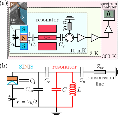
We demonstrate the proposed calibration scheme on a sample illustrated in Fig. 1. The device incorporates an SINIS junction which consists of two NIS junctions sharing a common normal-metal electrode. The normal-metal electrode of the tunnel junction is capacitively coupled to a half-wavelength superconducting coplanar-waveguide resonator. The resonator is further capacitively coupled to a transmission line from its other end, which conducts the signal to a three-stage amplification chain. The sample is placed in a dry dilution refrigerator at 10-mK base temperature. Reference Masuda et al., 2018 details the device fabrication.
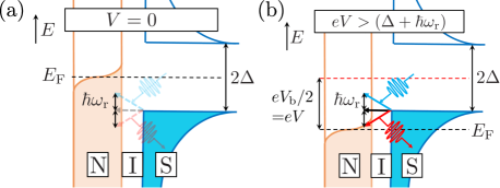
The bias voltage across the SINIS junction activates the photon-assisted electron tunneling events which control the mean photon number in the fundamental mode of the resonator. The photon number in turn determines the microwave power emitted to the transmission line. As described in Fig. 2, the electrons can tunnel through the NIS junction either elastically, i.e., without energy exchange with their electromagnetic environment, or inelastically by emitting or absorbing photons. In our setup, the resonator acts as the electromagnetic environment, and consequently the tunneling electrons absorb or emit photons at the resonance frequency of the resonator = 4.67 GHz. For vanishing bias voltage, both the elastic and inelastic tunneling events are suppressed due to the energy gap Bardeen et al. (1957); Dynes et al. (1984); Giaever (1960) of in the superconductor density of states as shown in Fig. 2(a). If the bias voltage is slightly below the energy gap, i.e., , electrons can tunnel through the junction by absorbing photons from the environment, which results in cooling of the resonator mode. In this work, we are mostly interested in the high-bias-voltage regime , where electron tunneling events involving photon emission are greatly enhanced, and hence the resonator mode heats up. The elevated temperature of the resonator mode leads to an increased radiative power into the transmission line, which enables us to calibrate the total gain of the amplification chain.We show below that the power and the bias voltage relate to each other through a simple equation in the high-bias regime. We apply the theory developed in Ref. Silveri et al., 2017 to describe the coupling between the resonator and the SINIS junction. In this model, we only take into account single-photon processes and we assume that the quasiparticle temperatures are equal in the normal-metal and superconducting electrodes. Furthermore, we assume sequential tunneling, i.e., that high-order processes are suppressed by the opaque tunnel barrier. Using the simplified electric circuit in Fig. 2(b) and Fermi’s golden rule, we can express the resonator damping rate and the effective temperature owing to the electron tunneling across the SINIS junction as Silveri et al. (2017)
| (1) | ||||
| (2) |
where is the asymptotic damping rate, is the normalized rate of forward tunneling, is the Boltzmann constant, is the reduced Planck constant, and is the voltage across a single NIS junction. We also have , where , is the tunneling resistance of a single NIS junction, and the remaining symbols are defined in Fig. 1(b). The normalized rate of forward tunneling is defined as
| (3) |
where is the energy gained by the tunneling electron, is the temperature of the normal-metal electrode, is the Fermi function, and is the Dynes density of states Dynes et al. (1984), which can be written as . The Dynes parameter describes the broadening of the superconductor energy gap, and is of the order of in a typical experimental scenario Pekola et al. (2010); Tan et al. (2017); Masuda et al. (2018).
In the high-bias regime, , we employ Eqs. (1) and (2) to derive the following approximations for the damping rate and the effective photon number of the engineered environment
| (4) | ||||
| (5) |
where we have utilized the Sommerfeld expansion Ashcroft and Mermin (1976). In addition, we have assumed that the Dynes parameter is small enough to be neglected at high bias voltages.
The resonator exchanges energy with the SINIS junction and with the transmission line. Furthermore, the resonator may be subjected to additional sources of dissipation which we model as a single excess reservoir. Each of these three types of dissipation can be modeled as a virtual transmission line Goetz et al. (2017b), which allows us to write the net power flow between the resonator and the th dissipative reservoir as
| (6) |
where is the damping rate of the resonator owing to the th reservoir, is the corresponding effective photon number, and is the resulting steady-state occupation of the resonator. Invoking the power balance and using Eqs. (4) and (5), the net power flow into the transmission line can be approximated as
| (7) |
where and are the damping rate and the effective photon number owing to the transmission line, respectively, whereas and are the corresponding quantities for the excess losses.
In our experiments, we measure the output power of the amplification chain , where is the total gain of the amplification chain including possible attenuation and losses, and is the noise power originating from the amplifiers. Consequently, we can determine the total gain by fitting a function of the form
| (8) |
to the measured power in the high bias regime , where are the fitting parameters. Using Eq. (7), the total gain can be expressed in terms of the leading-term coefficient as
| (9) |
Although we extract the total gain only from the coefficient , the other terms in Eq. (8) improve the fit substantially. The effective noise temperature of the amplification chain is obtained by examining the output power at zero bias voltage , where is practically zero with our device parameters and consequently
| (10) |
where is the bandwidth of the amplification chain.
In our experiments, we characterize the damping rates , , and with high accuracy leaving the parameter in Eq. (9) as the only free parameter in our model. To this end, we conduct standard microwave reflection measurements at different bias voltages . Based on the input-output theory Gardiner and Collett (1985), the voltage reflection coefficient of our system can be written as Clerk et al. (2010)
| (11) |
where is the probe frequency and is a complex-valued Fano resonance correction factor, which arises from the direct cross-talk of the dissipative reservoirsFan et al. (2003).
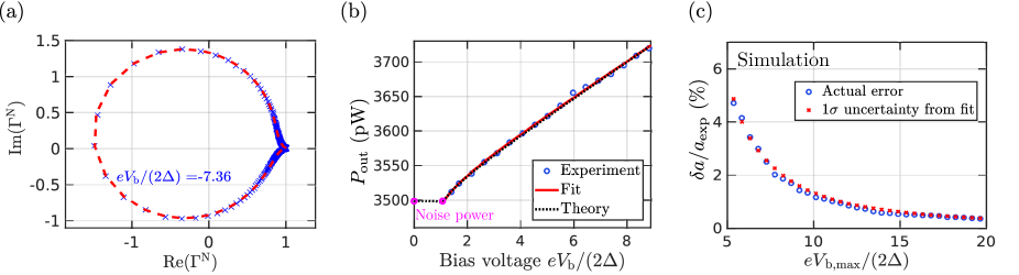
Since the bias voltage controls the coupling between the electromagnetic environment and the resonator, a Lamb shift arises for the resonance frequencySilveri et al. (2019) . The Lamb shift provides a convenient way of eliminating the unwanted background from the measurement data, namely, normalizing by the zero-bias measurement trace as shown in Fig. 3.(a). The ratio of two instances of Eq. (11) is fitted for every above the critical coupling point, , where the bias voltage-independent , , and the bias voltage-dependent are fitting parameters. Next, the asymptotic damping rate is extracted using Eq. (4). As a result, our characteristic damping rates are , , and , where the presented 1 uncertainties are obtained by the following method: First, an error circle is created that has a radius equal to the root mean square fit error and the center is located at , which correspond to the resonance of the bias voltage-dependent feature. Finally, confidence intervals of each parameter are individually determined by finding the boundaries such that the fitted is located within the error circle. The uncertainty of the excess damping rate is taken as the standard deviation of over the fitted voltage range.
After measuring the damping rates, we determine the total gain of the amplification chain by recording the microwave power at the output of the amplification chain for different bias voltages across the junction. To this end, we use a spectrum analyzer and numerically integrate the averaged spectral density around the resonance frequency GHz in the range 4.6–. From the data shown in Fig. 3(b), we observe a monotonous increase of the microwave power if the bias voltage exceeds the energy gap. We finally extract the total gain of the amplification chain by fitting Eq. (8) to the power data. Using Eq. (9) and the experimentally determined device parameters, the total gain of the amplification chain is estimated to be dB. Based on Eq. (10), the average noise temperature of our amplification chain is in the range 4.6–.
The relative uncertainty of the fitting parameter is extracted in the following way: we substitute the damping rates and the calibrated gain into Eq. (9) to determine the expected value for the fitting parameter . We then create a set of simulated power spectra for bias voltages up to . Fitting Eq. (8) to the corresponding power values, we extract the parameter and record the absolute error as a function of the maximum bias . In addition, we obtain the uncertainty from the fit and observe that it agrees with the error . In our experiments, we reach and therefore estimate the relative uncertainty of the fitting parameter . Combining the uncertainties of the damping rates , , , and the fitting parameter , we acquire for the uncertainty of the total gain.
In this paper, we have presented a calibration scheme for the total gain and noise temperature of a general amplification chain that comprises cryogenic and non-cryogenic amplifiers. The knowledge of the gain and noise temperature is important when operating quantum devices and other low-power microwave components. Currently, our setup allows the calibration of the total gain only at frequencies corresponding to a mode frequency of the resonator. The frequency range suitable for calibration can be expanded by placing a superconducting quantum interference device (SQUID) in the resonator Partanen et al. (2018); Sandberg et al. (2008). In the future, we aim at benchmarking the accuracy of the proposed gain calibration scheme against a method utilizing a superconducting qubit in a resonator. By employing the ac Stark shift, we can determine the photon number in the resonator Wallraff et al. (2004); Schuster et al. (2005) and thus the total gain of the amplification chain.
Acknowledgements.
This project has received funding from the European Union’s Horizon 2020 Research and Innovation Programme under the Marie Skłodowska-Curie Grant Agreement No. 795159 and under the European Research Council Consolidator Grant No. 681311 (QUESS), from the Academy of Finland Centre of Excellence in Quantum Technology Grant No. 312300 and No. 305237, from JST ERATO Grant No. JPMJER1601, from JSPS KAKENHI Grant No. 18K03486, and from the Vilho, Yrjö and Kalle Väisälä Foundation. We acknowledge the provision of facilities and technical support by Aalto University at OtaNano - Micronova Nanofabrication Centre.References
- Wallraff et al. (2004) A. Wallraff, D. I. Schuster, A. Blais, L. Frunzio, R.-S. Huang, J. Majer, S. Kumar, S. M. Girvin, and R. J. Schoelkopf, Nature 431, 162 (2004).
- Niemczyk et al. (2010) T. Niemczyk, F. Deppe, H. Huebl, E. Menzel, F. Hocke, M. Schwarz, J. Garcia-Ripoll, D. Zueco, T. Hümmer, E. Solano, et al., Nat. Phys. 6, 772 (2010).
- Devoret and Schoelkopf (2013) M. H. Devoret and R. J. Schoelkopf, Science 339, 1169 (2013).
- Blais et al. (2004) A. Blais, R.-S. Huang, A. Wallraff, S. M. Girvin, and R. J. Schoelkopf, Phys. Rev. A 69, 062320 (2004).
- Majer et al. (2007) J. Majer, J. Chow, J. Gambetta, J. Koch, B. Johnson, J. Schreier, L. Frunzio, D. Schuster, A. Houck, A. Wallraff, et al., Nature 449, 443 (2007).
- Sillanpää et al. (2007) M. A. Sillanpää, J. I. Park, and R. W. Simmonds, Nature 449, 438 (2007).
- DiCarlo et al. (2009) L. DiCarlo, J. Chow, J. Gambetta, L. S. Bishop, B. Johnson, D. Schuster, J. Majer, A. Blais, L. Frunzio, S. Girvin, et al., Nature 460, 240 (2009).
- DiCarlo et al. (2010) L. DiCarlo, M. D. Reed, L. Sun, B. R. Johnson, J. M. Chow, J. M. Gambetta, L. Frunzio, S. M. Girvin, M. H. Devoret, and R. J. Schoelkopf, Nature 467, 574 (2010).
- Brecht et al. (2016) T. Brecht, W. Pfaff, C. Wang, Y. Chu, L. Frunzio, M. H. Devoret, and R. J. Schoelkopf, npj Quantum Inf. 2, 16002 (2016).
- Barends et al. (2014) R. Barends, J. Kelly, A. Megrant, A. Veitia, D. Sank, E. Jeffrey, T. C. White, J. Mutus, A. G. Fowler, B. Campbell, et al., Nature 508, 500 (2014).
- Córcoles et al. (2015) A. D. Córcoles, E. Magesan, S. J. Srinivasan, A. W. Cross, M. Steffen, J. M. Gambetta, and J. M. Chow, Nat. Commun. 6, 6979 (2015).
- Song et al. (2017) C. Song, K. Xu, W. Liu, C.-p. Yang, S.-B. Zheng, H. Deng, Q. Xie, K. Huang, Q. Guo, L. Zhang, et al., Phys. Rev. Lett. 119, 180511 (2017).
- Wang et al. (2011) D. S. Wang, A. G. Fowler, and L. C. Hollenberg, Phys. Rev. A 83, 020302 (2011).
- Kelly et al. (2015) J. Kelly, R. Barends, A. Fowler, A. Megrant, E. Jeffrey, T. White, D. Sank, J. Mutus, B. Campbell, Y. Chen, et al., Nature 519, 66 (2015).
- Ofek et al. (2016) N. Ofek, A. Petrenko, R. Heeres, P. Reinhold, Z. Leghtas, B. Vlastakis, Y. Liu, L. Frunzio, S. Girvin, L. Jiang, et al., Nature 536, 441 (2016).
- Mallet et al. (2009) F. Mallet, F. R. Ong, A. Palacios-Laloy, F. Nguyen, P. Bertet, D. Vion, and D. Esteve, Nat. Phys. 5, 791 (2009).
- Dewes et al. (2012) A. Dewes, F. Ong, V. Schmitt, R. Lauro, N. Boulant, P. Bertet, D. Vion, and D. Esteve, Phys. Rev. Lett. 108, 057002 (2012).
- Lin et al. (2013) Z. Lin, K. Inomata, W. Oliver, K. Koshino, Y. Nakamura, J. Tsai, and T. Yamamoto, Appl. Phys. Lett. 103, 132602 (2013).
- Riste et al. (2013) D. Riste, M. Dukalski, C. Watson, G. De Lange, M. Tiggelman, Y. M. Blanter, K. W. Lehnert, R. Schouten, and L. DiCarlo, Nature 502, 350 (2013).
- Heinsoo et al. (2018) J. Heinsoo, C. K. Andersen, A. Remm, S. Krinner, T. Walter, Y. Salathé, S. Gasparinetti, J.-C. Besse, A. Potočnik, A. Wallraff, and C. Eichler, Phys. Rev. Appl. 10, 034040 (2018).
- Ikonen et al. (2019) J. Ikonen, J. Goetz, J. Ilves, A. Keränen, A. M. Gunyhó, M. Partanen, K. Y. Tan, L. Grönberg, V. Vesterinen, S. Simbierowicz, J. Hassel, and M. Möttönen, Phys. Rev. Lett. 122, 080503 (2019).
- Macklin et al. (2015) C. Macklin, K. OflBrien, D. Hover, M. Schwartz, V. Bolkhovsky, X. Zhang, W. Oliver, and I. Siddiqi, Science 350, 307 (2015).
- Yurke et al. (1988) B. Yurke, P. Kaminsky, R. Miller, E. Whittaker, A. Smith, A. Silver, and R. Simon, Phys. Rev. Lett. 60, 764 (1988).
- Yamamoto et al. (2008) T. Yamamoto, K. Inomata, M. Watanabe, K. Matsuba, T. Miyazaki, W. Oliver, Y. Nakamura, and J. Tsai, Appl. Phys. Lett. 93, 042510 (2008).
- Castellanos-Beltran and Lehnert (2007) M. Castellanos-Beltran and K. Lehnert, Appl. Phys. Lett. 91, 083509 (2007).
- Pogorzalek et al. (2017) S. Pogorzalek, K. G. Fedorov, L. Zhong, J. Goetz, F. Wulschner, M. Fischer, P. Eder, E. Xie, K. Inomata, T. Yamamoto, Y. Nakamura, A. Marx, F. Deppe, and R. Gross, Phys. Rev. App. 8, 024012 (2017).
- Kokkoniemi et al. (2018) R. Kokkoniemi, J. Govenius, V. Vesterinen, R. Lake, A. Gunyhó, K. Tan, S. Simbierowicz, L. Grönberg, J. Lehtinen, M. Prunnila, et al., arXiv preprint arXiv:1806.09397 (2018).
- Goetz et al. (2017a) J. Goetz, S. Pogorzalek, F. Deppe, K. G. Fedorov, P. Eder, M. Fischer, F. Wulschner, E. Xie, A. Marx, and R. Gross, Phys. Rev. Lett. 118, 103602 (2017a).
- Mariantoni et al. (2010) M. Mariantoni, E. P. Menzel, F. Deppe, M. A. Caballero, A. Baust, T. Niemczyk, E. Hoffmann, E. Solano, A. Marx, and R. Gross, Phys. Rev. Lett. 105, 133601 (2010).
- Yfa (2001) Noise Figure Measurement Accuracy –- The Y-Factor Method, Agilent Technologies (2001), application note 57-2.
- Fernandez (1998) J. Fernandez, progress report 42-135 (1998).
- Blanter and Büttiker (2000) Y. M. Blanter and M. Büttiker, Phys. Rep 336, 1 (2000).
- Spietz et al. (2003) L. Spietz, K. Lehnert, I. Siddiqi, and R. Schoelkopf, Science 300, 1929 (2003).
- Chang et al. (2016) S.-W. Chang, J. Aumentado, W.-T. Wong, and J. C. Bardin, in Microwave Symposium (IMS), 2016 IEEE MTT-S International (IEEE, 2016) pp. 1–4.
- Aassime et al. (2001) A. Aassime, G. Johansson, G. Wendin, R. Schoelkopf, and P. Delsing, Phys. Rev. Lett. 86, 3376 (2001).
- Tan et al. (2017) K. Y. Tan, M. Partanen, R. E. Lake, J. Govenius, S. Masuda, and M. Möttönen, Nat. Commun. 8, 15189 (2017).
- Masuda et al. (2018) S. Masuda, K. Y. Tan, M. Partanen, R. E. Lake, J. Govenius, M. Silveri, H. Grabert, and M. Möttönen, Sci. Rep. 8, 3966 (2018).
- Kafanov et al. (2009) S. Kafanov, A. Kemppinen, Y. A. Pashkin, M. Meschke, J. Tsai, and J. P. Pekola, Phys. Rev. Lett. 103, 120801 (2009).
- Gasparinetti et al. (2015) S. Gasparinetti, K. Viisanen, O.-P. Saira, T. Faivre, M. Arzeo, M. Meschke, and J. Pekola, Phys. Rev. Appl. 3, 014007 (2015).
- Silveri et al. (2017) M. Silveri, H. Grabert, S. Masuda, K. Y. Tan, and M. Möttönen, Phys. Rev. B 96, 094524 (2017).
- Silveri et al. (2019) M. Silveri, S. Masuda, V. Sevriuk, K. Y. Tan, M. Jenei, E. Hyyppä, F. Hassler, M. Partanen, J. Goetz, R. E. Lake, L. Grönberg, and M. Möttönen, Nat. Phys. (2019), 10.1038/s41567-019-0449-0.
- Bardeen et al. (1957) J. Bardeen, L. N. Cooper, and J. R. Schrieffer, Phys. Rev. 108, 1175 (1957).
- Dynes et al. (1984) R. Dynes, J. Garno, G. Hertel, and T. Orlando, Phys. Rev. Lett. 53, 2437 (1984).
- Giaever (1960) I. Giaever, Phys. Rev. Lett. 5, 147 (1960).
- Pekola et al. (2010) J. P. Pekola, V. Maisi, S. Kafanov, N. Chekurov, A. Kemppinen, Y. A. Pashkin, O.-P. Saira, M. Möttönen, and J. Tsai, Phys. Rev. Lett. 105, 026803 (2010).
- Ashcroft and Mermin (1976) N. W. Ashcroft and N. D. Mermin, Solid state physics (Saunders College, Philadelphia, 1976).
- Goetz et al. (2017b) J. Goetz, F. Deppe, P. Eder, M. Fischer, M. Müting, J. Puertas Martínez, S. Pogorzalek, F. Wulschner, E. Xie, K. G. Fedorov, A. Marx, and R. Gross, Quant. Sci. Tech. 2, 025002 (2017b).
- Gardiner and Collett (1985) C. Gardiner and M. Collett, Phys. Rev. A 31, 3761 (1985).
- Clerk et al. (2010) A. A. Clerk, M. H. Devoret, S. M. Girvin, F. Marquardt, and R. J. Schoelkopf, Rev. Mod. Phys. 82, 1155 (2010).
- Fan et al. (2003) S. Fan, W. Suh, and J. D. Joannopoulos, J. Opt. Soc. Am. A 20, 569 (2003).
- Partanen et al. (2018) M. Partanen, K. Y. Tan, S. Masuda, J. Govenius, R. E. Lake, M. Jenei, L. Grönberg, J. Hassel, S. Simbierowicz, V. Vesterinen, et al., Sci. Rep. 8, 6325 (2018).
- Sandberg et al. (2008) M. Sandberg, C. Wilson, F. Persson, T. Bauch, G. Johansson, V. Shumeiko, T. Duty, and P. Delsing, Appl. Phys. Lett. 92, 203501 (2008).
- Schuster et al. (2005) D. Schuster, A. Wallraff, A. Blais, L. Frunzio, R.-S. Huang, J. Majer, S. Girvin, and R. Schoelkopf, Phys. Rev. Lett. 94, 123602 (2005).