Phonon and electron transport in Janus monolayers based on InSe
Abstract
We systematically investigated the phonon and electron transport properties of monolayer InSe and its Janus derivatives including monolayer In2SSe and In2SeTe by first-principles calculations. The breaking of mirror symmetry produces a distinguishable peak in the Raman spectra of monolayer In2SSe and In2SeTe. The room-temperature thermal conductivity () of monolayer InSe, In2SSe and In2SeTe is 44.6, 46.9, and 29.9 W/(m K), respectively. There is a competition effect between atomic mass, phonon group velocity and phonon lifetime. The can be further effectively modulated by sample size for the purpose of thermoelectric applications. Meanwhile, monolayer In2SeTe exhibits a direct band and higher electron mobility than that of monolayer InSe, due to the smaller electron effective mass caused by tensile strain on the Se side. These results indicate that 2D Janus group-III chalcogenides can provide a platform to design the new electronic, optoelectronic and thermoelectric devices.
pacs:
63.22.-m, 65.40.-b, 63.20.kr, 72.20.FrIndium Selenide (InSe), as an experimentally accessible layered group-III metal chalcogenide, has been receiving much attention. Boukhvalov et al. (2017) The synthesized few-layer InSe exhibits small electron effective mass ( 0.14 ) and room-temperature electron mobility () higher than cm2/(Vs). Bandurin et al. (2017); Sucharitakul et al. (2015) Nano-devices based on two dimensional (2D) InSe had good ambient stability. Nan et al. (2018) In addition, 2D InSe holds promise for the application of bendable photodetectors with broadband response, Tamalampudi et al. (2014) 2D ferromagnets, Iordanidou et al. (2018) excitonic dynamics, Dey et al. (2014) magneto-optical effects Feng, Guo, and Yao (2017) and topological insulator. Zhou et al. (2018)
Recently, a new Janus-type monolayer MoSSe has been synthesized through the replacement of the S atoms at one side of monolayer MoS2 by Se atoms. Lu et al. (2017); Li, Cheng, and Huang (2018) Both band gap and thermal conductivity of monolayer MoSSe are between that of monolayer MoS2 and MoSe2. Guo (2018) As far as Janus structures based on 2D InSe are concerned, Kandemir et al. found that the band structure of the monolayer In2SSe was formed by the superposition of the strained band structures of the binary analog single layers. Kandemir and Sahin (2018) Guo et al. predicted that the 2D Janus group-III chalcogenides had enhanced piezoelectric coefficients compared to that of perfect ones. Guo et al. (2017) The out-of-plane symmetry breaking in 2D Janus structures can also induce unusual properties such as enhanced Rashba effect, Xia et al. (2018) catalytic activity for hydrogen evolution, Er et al. (2018) the valley polarization upon magnetic doping, Peng et al. (2018) excitons with long lifetime Jin et al. (2018) and so on. Besides the electronic properties, thermal properties become a crucial issue for the device’s performance, as on-going miniaturization of electronic devices. For example, a high and low is desirable for the efficient heat dissipation in integrated electronic devices and high conversion efficiency of thermoelectrics, respectively. Hochbaum et al. (2008) Nissimagoudar et al. predicted that the of monolayer InSe can be effectively reduced by boundary scattering. Nissimagoudar et al. (2017) Pandey et al. calculated the of monolayer GaS, GaSe, and InSe, and found that the increase of mass gave both decreasing acoustic phonon velocities and increasing scattering of heat-carrying modes. Pandey, Parker, and Lindsay (2017) The thermal properties of 2D materials can be tuned by doping or alloying, Zhou et al. (2016) strain, Deng, Sumant, and Berry (2018) chemical functionalization Wang et al. (2017) and so on, expanding its application prospect. Therefore, Janus structures can not only expand the family of 2D materials but also offer another way to modulate the thermal properties of 2D materials. Though much efforts have been devoted to the physical properties of 2D Janus group-III chalcogenides, the mechanism of its phonon and electron transport are still not well understood.
In this work, we studied the structural, optical and transport properties of monolayer InSe, In2SSe and In2SeTe by first-principles calculations. Because of the breaking of mirror symmetry, Raman spectra of Janus structures exhibit a special peak compared to that of monolayer InSe. The of monolayer In2SSe and In2SeTe is larger and smaller than that of monolayer InSe. The mechanism of heat transport are carefully analyzed. At last, we calculated the electron mobility of monolayer InSe and its Janus structures. The of monolayer In2SeTe is superior to that of monolayer InSe.
| (Å) | (Å) | (Å) | (Å) | (cm-1) | ||||
|---|---|---|---|---|---|---|---|---|
| InSe | 4.093 | 2.817 | 2.690 | 5.386 | 2.147 | 109 ()[110] Zhou et al. (2018) | 178 ()[178] Zhou et al. (2018) | 223 ()[225] Zhou et al. (2018) |
| In2SSe | 4.015 | 2.819 | 2.671/2.585 | 5.289 | 2.297 | 124 () | 214 () | 257 () |
| In2SeTe | 4.244 | 2.815 | 2.729/2.856 | 5.483 | 1.967 | 96 () | 167 () | 211 () |
Based on the phonon Boltzmann transport function, lattice thermal conductivity is estimated by Li et al. (2014)
| (1) |
where and are Cartesian indices. and is the number of point and volume of the unit cell, respectively. , and is the specific capacity, group velocity and lifetime in the single-mode relaxation time approximation (RTA) of the phonon with wavevector and branch index , respectively. The phonon lifetime was estimated by combining the anharmonic scattering, isotopic impurities scattering and boundary scattering according to the Matthiessen rule Li et al. (2014)
| (2) |
where boundary roughness scattering rate is with be the sample size. All the computational details are given in the supplementary material (SM).
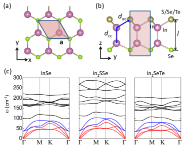
Monolayer InSe consists of a quadruple layer in a stacking sequence of Se-In-In-Se and its lattice has crystal symmetry (see Fig. 1(a) and 1(b)). Janus monolayer In2SSe and In2SeTe are built by replacing top-layer Se by S or Te atoms. Janus structures have crystal symmetry without out-of-plane mirror symmetry (). The thickness of monolayer was estimated by the distance between the atoms on the outmost layer (see Fig. 1(c)). The optimized structural parameters are listed in Table 1. The cation-cation bonding () have a slight change compared to that of monolayer InSe. The anion-cation bonding length () of In2SSe and In2SeTe is smaller and larger than that of monolayer InSe, respectively, due to the smaller and larger atomic radius of S and Te atom than that of Se atom. As a result, one side of Janus structures experiences a tensile or compressive strain, compared to its perfect binary analogs. Kandemir and Sahin (2018) For example, the bonding length of on Se side and on Te side of monolayer In2SeTe is larger and smaller than that of monolayer InSe and InTe ( = 2.890 Å in our calculation), respectively (see Table 1).
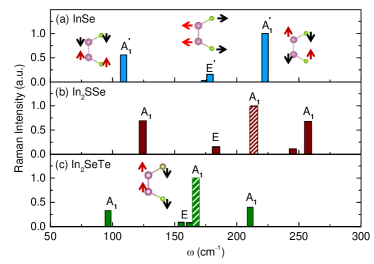
Monolayer InSe and its Janus derivatives are semiconductors (see Fig. S2). Figure 1(c) displays the phonon dispersive relations and indicates their structural stability. The acoustic branches consist of the longitudinal (LA) branch, transverse (TA) branch and flexural branch (ZA) branch. Acoustic branches intersect with optical branches. The phonon modes at the point of monolayer InSe are decomposed into according to the analysis of group theory. , and modes are Raman active. The calculated Raman spectra exhibits three prominent peaks (see Fig. 2(a)). Two Raman peaks at frequencies of 109 and 223 cm-1 arise from two out-of-plane modes and a smaller peak at =178 cm-1 originates from in-plane mode, consistent with the previous work (see Table 1). Zhou et al. (2018)
On the other side, the -point phonon modes of Janus monolayer In2SSe and In2SeTe are decomposed into . All the optical modes are Raman active. There are two prominent peaks at the low- and high-frequency zone (see Fig. 2(b) and 2(c)). Its eigenvectors are similar to that of two peak of monolayer InSe. In addition, a conspicuous mode, which is absent in monolayer InSe, appears in the intermediate frequency zone (labeled by slant lines). The phonon mode with the similar eigen-displacements (see inset of Fig. 2(c)) in monolayer InSe belongs to representation. The change of polarizability with corresponding normal coordinate at the equilibrium configuration is zero due to the mirror symmetry, so the mode is Raman inactive. Therefore, the raman peak due to the breaking of mirror symmetry can serve as the characteristic signal of 2D In2SSe and In2SeTe during its synthesis.
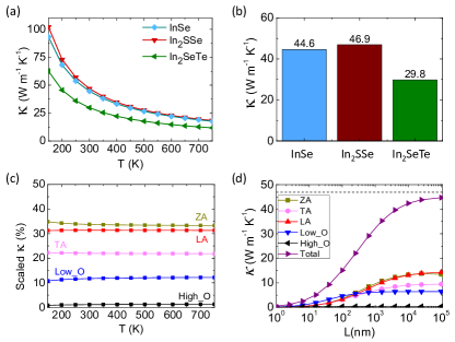
The of monolayer InSe and its Janus derivatives in the temperature range of T = 150750 K are shown in Fig. 3(a). At T = 300 K, the of monolayer InSe and In2SSe is estimated as 44.6 and 46.9 W/(mK), respectively (see Fig. 3(b)), which is comparable to that of semiconductor GaAs (45 W/(m K)), Morelli and A. (2006) few-layer MoS2 (4050 W/(m K)) Jo et al. (2014) and few-layer black phosphorus (1020 W/(m K)). Luo et al. (2015) The result of monolayer InSe agrees with previous Pandey’s work. Pandey, Parker, and Lindsay (2017) In contrast, monolayer In2SeTe with heavier atomic mass has a smaller of 29.8 W/(mK).
Besides the acoustic branches, low-frequency optical (-) branches (labeled by blue in Fig. 1(e)) also make a non-negligible contribution to the of monolayer InSe and its Janus derivatives (see Fig. 3(c)). The large phonon group velocity of - branches is the main reason. In contrast, only the acoustic phonons are considered in the heat transport of conventional semiconductors. Meanwhile, the heat is mainly carried by phonons with frequencies less than 100 cm-2, since the group velocities of higher optical modes are small.
Considering the limited sample size (), the size effects of and its contribution from different branches are discussed in the range of diffusive thermal transport. The representative result of monolayer In2SSe is displayed in Fig. 3(d). The results of monolayer InSe and In2SeTe are similar. At room temperature, the phonon mean free path (MFP) of monolayer In2SSe is about nm, which is mainly determined by the MFP of LA and ZA phonons. The can be decreased by 90% as the decrease down to 10 nm. That indicates that nanostructuring might be an effective method to reduce the of 2D group-III chalcogenide for the thermoelectric applications.
To give a more deep understand of heat transport in monolayer InSe and its Janus structures, we analyzed every term in determining the in Eq. 1. The mode group velocity in the frequency zone of cm-1 are displayed in Fig. 4(a). The overall of monolayer In2SSe and In2SeTe is higher and lower than that of monolayer InSe, due to the smaller and larger atomic mass than that of InSe, respectively. Figure 4(b) shows the mode relaxation time at room temperature. The overall of monolayer InSe, In2SSe and In2SeTe have the same order of magnitude at low-frequency zone of cm-1. However, the of Janus structures is smaller than that of monolayer InSe at the frequency between 25 and 75 cm-1. It was found that the anharmonic scattering () dominate the total phonon lifetime. In contrast, the isotopic impurities scattering, which is inversely proportional to atomic mass, Li et al. (2014) has a small influence on , e.g. the room-temperature of monolayer In2SSe will increase only by 1.26% if we excluded the from the total scattering rate .
The anharmonic depends on the square of Grüneisen parameter and weighted phase space . Li et al. (2014) The former and latter one represents the anharmonicity strength and the number of channels available for a phonon to get scattered, respectively. Li and Mingo (2015); Li et al. (2014) The increase of or has a decreased effect on .
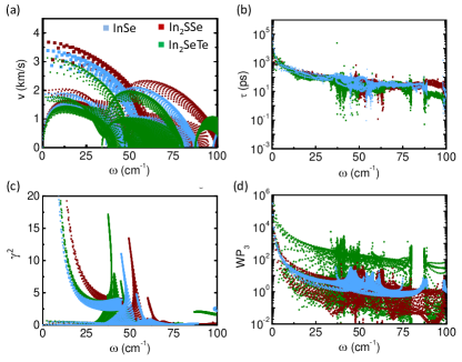
The overall of monolayer InSe is smaller than that of its Janus derivatives (see Fig. 4(c)). The breaking of mirror symmetry in Janus structures leads to the asymmetric chemical bonding and charge density distribution along the out-of-plane direction, which will increase the bond anharmonicity. Zhang et al. (2017); Wu et al. (2016) Figure 4(d)) shows that the sequential of from high to low is (In2SeTe)(InSe)(In2SSe). of monolayer InSe, which has the mirror symmetry, is between that of monolayer In2SSe and In2SeTe. The phase space for anharmonic scattering decreases as the overall phonon frequency scale increases (see Fig. 1(e)), consistent with the observation in many bulk materials. Lindsay and Broido (2008) As a result, of monolayer InSe is larger than that of monolayer In2SSe at frequency between 50 and 65 cm-1 (see Fig. 4(b) and Fig. S3), due to the integral effect of , and . In the end, monolayer In2SSe, with smaller atomic mass, larger but a smaller , has a slightly larger than that of monolayer InSe. On the other side, the larger atomic mass, smaller , larger and leads to the smaller and in monolayer In2SeTe than InSe.
Besides the heat transport, we also calculated the carrier mobility based on the deformation potential theory (see computational details and Fig. S4 in SM). Bardeen and Shockley (1950) The band structure indicates that electron effective mass is smaller than hole one which has Mexican-hat valence band edge (see Fig. S2), consistent with previous work. Guo et al. (2017) The parameters involved in electron mobility are shown in Table 2. The order of from large to small is In2SSeInSeIn2SeTe), consistent with the order of and (see Table 1 and Fig. 4(c)).
The electron effective mass of monolayer In2SSe and In2SeTe is larger and smaller than that of monolayer InSe, respectively. The orbital analysis indicates that the electronic states at conduction band minimum (CBM) of monolayer InSe is dominated by In- orbital with symmetry spatial distribution (see Fig. S5). In contrast, the electronic states at CBM of monolayer In2SSe and In2SeTe is mainly composed of orbital of In atom on the S and Se side, respectively. Taking monolayer In2SeTe as an example, the Se side experiences aforementioned tensile strain compared to that of monolayer InSe. Actually, if we applied a biaxial tensile strain of to the lattice of monolayer InSe, the becomes close to that of monolayer In2SeTe. Meanwhile, the changes from 0.188 to 0.174 , consistent with the of In2SeTe (Table 2). Similarly, of monolayer In2SSe is about 2% larger than that of monolayer InS. The calculated of monolayer InS under 2% tensile strain is 0.227 , which can also explain the larger of monolayer In2SSe than that of monolayer InSe.
The of monolayer In2SSe and In2SeTe is smaller and larger than that of monolayer InSe, which can be attributed to larger and smaller , respectively. Moreover, monolayer In2SeTe has a direct band gap of 1.8 eV and thereby is more favorable for optoelectronics application than monolayer InSe and In2SSe which have indirect band gaps (see Fig. S2),
| Type | |||||
|---|---|---|---|---|---|
| InSe | 0.181 | 0.182 | 49.21 | 5.815 | 943.3 |
| [0.177] Chang et al. (2019) | [0.182] Chang et al. (2019) | ||||
| In2SSe | 0.211 | 0.212 | 52.69 | 5.331 | 884.8 |
| In2SeTe | 0.175 | 0.176 | 44.22 | 5.075 | 1190.6 |
Based on the first-principles calculations, we investigated the thermal and electronic transport properties of monolayer InSe, In2SSe and In2SeTe. One side of monolayer In2SSe and In2SeTe undergo tensile or compressive strain. A distinguishable peak in the Raman spectra of monolayer In2SSe and In2SeTe was identified due to the breaking of mirror symmetry. The room-temperature of monolayer InSe, In2SSe and In2SeTe is 44.6, 46.9 and 29.8 W/(mK), respectively. Though with smaller atomic mass, the of monolayer In2SSe is comparable to that of monolayer InSe, due to the competition effect between phonon group velocity and lifetime. Moreover, the electron mobility of monolayer In2SeTe is higher than that of monolayer InSe, due to that smaller electron effective mass and deformation potential, respectively. Our work facilitates the understanding of the heat and carrier transport properties of 2D Janus group-III chalcogenides and offers the theoretical support to the corresponding device designment in future.
Supplementary Material
See Supplemental Material for the computational details; The convergence test of with respect to the Q-grid size and the force cut-off; The band structure and the distribution of electronic states; The fitting parameters for the mobility.
Acknowledgements.
The numerical calculations in this paper have been done on the supercomputing system in the High Performance Computing Center of Yanshan University. This work was supported by the the Specialized Research Fund for the Doctoral Program of Higher Education of China (Grant No.2018M631760), the Project of Heibei Educational Department, China (No. ZD2018015 and QN2018012).References
- Boukhvalov et al. (2017) D. W. Boukhvalov, B. Gürbulak, S. Duman, L. Wang, A. Politano, L. S. Caputi, G. Chiarello, and A. Cupolillo, “The advent of indium selenide: Synthesis, electronic properties, ambient stability and applications,” Nanomaterials 7, 372 (2017).
- Bandurin et al. (2017) D. A. Bandurin, A. V. Tyurnina, L. Y. Geliang, A. Mishchenko, V. Zólyomi, S. V. Morozov, R. K. Kumar, R. V. Gorbachev, Z. R. Kudrynskyi, S. Pezzini, et al., “High electron mobility, quantum hall effect and anomalous optical response in atomically thin InSe,” Nat. Nanotechnol. 12, 223–227 (2017).
- Sucharitakul et al. (2015) S. Sucharitakul, N. J. Goble, U. R. Kumar, R. Sankar, Z. A. Bogorad, F.-C. Chou, Y.-T. Chen, and X. P. A. Gao, “Intrinsic electron mobility exceeding 103 cm2/(vs) in multilayer InSe FETs,” Nano Lett. 15, 3815–3819 (2015).
- Nan et al. (2018) H. Nan, S. Guo, S. Cai, Z. Chen, A. Zafar, X. Zhang, X. Gu, S. Xiao, and Z. Ni, “Producing air-stable InSe nanosheet through mild oxygen plasma treatment,” Semicond. Sci. Technol. 33, 074002 (2018).
- Tamalampudi et al. (2014) S. R. Tamalampudi, Y.-Y. Lu, R. Kumar U., R. Sankar, C.-D. Liao, K. Moorthy B., C.-H. Cheng, F. C. Chou, and Y.-T. Chen, “High performance and bendable few-layered InSe photodetectors with broad spectral response,” Nano Lett. 14, 2800–2806 (2014).
- Iordanidou et al. (2018) K. Iordanidou, M. Houssa, J. Kioseoglou, V. V. Afanas’ev, A. Stesmans, and C. Persson, “Hole-doped 2D InSe for spintronic applications,” ACS Appl. Nano Mater. 1, 6656–6665 (2018).
- Dey et al. (2014) P. Dey, J. Paul, N. Glikin, Z. D. Kovalyuk, Z. R. Kudrynskyi, A. H. Romero, and D. Karaiskaj, “Mechanism of excitonic dephasing in layered InSe crystals,” Phys. Rev. B 89, 125128 (2014).
- Feng, Guo, and Yao (2017) W. Feng, G.-Y. Guo, and Y. Yao, “Tunable magneto-optical effects in hole-doped group-III A metal-monochalcogenide monolayers,” 2D Mater. 4, 015017 (2017).
- Zhou et al. (2018) S. Zhou, C.-C. Liu, J. Zhao, and Y. Yao, “Monolayer group-III monochalcogenides by oxygen functionalization: a promising class of two-dimensional topological insulators,” npj Quantum Mater. 3, 16 (2018).
- Lu et al. (2017) A.-Y. Lu, H. Zhu, J. Xiao, C.-P. Chuu, Y. Han, M.-H. Chiu, C.-C. Cheng, C.-W. Yang, K.-H. Wei, Y. Yang, Y. Wang, D. Sokaras, D. Nordlund, P. Yang, D. A. Muller, M.-Y. Chou, X. Zhang, and L.-J. Li, “Janus monolayers of transition metal dichalcogenides,” Nat. Nanotechnol. 12, 744 (2017).
- Li, Cheng, and Huang (2018) R. Li, Y. Cheng, and W. Huang, “Recent progress of Janus 2D transition metal chalcogenides: From theory to experiments,” Small 14, 1802091 (2018).
- Guo (2018) S.-D. Guo, “Phonon transport in Janus monolayer MoSSe: a first-principles study,” Phys. Chem. Chem. Phys. 20, 7236–7242 (2018).
- Kandemir and Sahin (2018) A. Kandemir and H. Sahin, “Janus single layers of In2SSe: A first-principles study,” Phys. Rev. B 97, 155410 (2018).
- Guo et al. (2017) Y. Guo, S. Zhou, Y. Bai, and J. Zhao, “Enhanced piezoelectric effect in Janus group-III chalcogenide monolayers,” Appl. Phys. Lett. 110, 163102 (2017).
- Xia et al. (2018) C. Xia, W. Xiong, J. Du, T. Wang, Y. Peng, and J. Li, “Universality of electronic characteristics and photocatalyst applications in the two-dimensional Janus transition metal dichalcogenides,” Phys. Rev. B 98, 165424 (2018).
- Er et al. (2018) D. Er, H. Ye, N. C. Frey, H. Kumar, J. Lou, and V. B. Shenoy, “Prediction of enhanced catalytic activity for hydrogen evolution reaction in Janus transition metal dichalcogenides,” Nano Lett. 18, 3943–3949 (2018).
- Peng et al. (2018) R. Peng, Y. Ma, S. Zhang, B. Huang, and Y. Dai, “Valley polarization in Janus single-layer MoSSe via magnetic doping,” J. Phys. Chem. Lett. 9, 3612–3617 (2018).
- Jin et al. (2018) H. Jin, T. Wang, Z.-R. Gong, C. Long, and Y. Dai, “Prediction of an extremely long exciton lifetime in a Janus-MoSTe monolayer,” Nanoscale 10, 19310–19315 (2018).
- Hochbaum et al. (2008) A. I. Hochbaum, R. Chen, R. D. Delgado, W. Liang, E. C. Garnett, M. Najarian, A. Majumdar, and P. Yang, “Enhanced thermoelectric performance of rough silicon nanowires,” Nature 451, 163–167 (2008).
- Nissimagoudar et al. (2017) A. S. Nissimagoudar, J. Ma, Y. Chen, and W. Li, “Thermal transport in monolayer InSe,” J. Phys.: Condens. Matter 29, 335702 (2017).
- Pandey, Parker, and Lindsay (2017) T. Pandey, D. S. Parker, and L. Lindsay, “Ab initio phonon thermal transport in monolayer InSe, GaSe, GaS, and alloys,” Nanotechnology 28, 455706 (2017).
- Zhou et al. (2016) Y. Zhou, Z.-X. Guo, H.-Y. Cao, S.-Y. Chen, H.-J. Xiang, and X.-G. Gong, “Thermal conductivity of disordered two-dimensional binary alloys,” Nanoscale 8, 17815–17819 (2016).
- Deng, Sumant, and Berry (2018) S. Deng, A. V. Sumant, and V. Berry, “Strain engineering in two-dimensional nanomaterials beyond graphene,” Nano Today 22, 14 – 35 (2018).
- Wang et al. (2017) Y. Wang, N. Xu, D. Li, and J. Zhu, “Thermal properties of two dimensional layered materials,” Adv. Funct. Mater. 27, 1604134 (2017).
- Li et al. (2014) W. Li, J. Carrete, N. A. Katcho, and N. Mingo, “ShengBTE: A solver of the boltzmann transport equation for phonons,” Comput. Phys. Commun. 185, 1747 – 1758 (2014).
- Morelli and A. (2006) D. T. Morelli and S. G. A., High Thermal Conductivity Materials, edited by S. L. Shinde and J. Goela (Springer-Verlag New York, 2006).
- Jo et al. (2014) I. Jo, M. T. Pettes, E. Ou, W. Wu, and L. Shi, “Basal-plane thermal conductivity of few-layer molybdenum disulfide,” Appl. Phys. Lett. 104, 201902 (2014).
- Luo et al. (2015) Z. Luo, J. Maassen, Y. Deng, Y. Du, R. P. Garrelts, M. S. Lundstrom, P. D. Ye, and X. Xu, “Anisotropic in-plane thermal conductivity observed in few-layer black phosphorus,” Nat. Commun. 6, 8572 EP – (2015), article.
- Li and Mingo (2015) W. Li and N. Mingo, “Ultralow lattice thermal conductivity of the fully filled skutterudite YbFe4Sb12 due to the flat avoided-crossing filler modes,” Phys. Rev. B 91, 144304 (2015).
- Zhang et al. (2017) A.-X. Zhang, J.-T. Liu, S.-D. Guo, and H.-C. Li, “Strain effects on phonon transport in antimonene investigated using a first-principles study,” Phys. Chem. Chem. Phys. 19, 14520–14526 (2017).
- Wu et al. (2016) X. Wu, V. Varshney, J. Lee, T. Zhang, J. L. Wohlwend, A. K. Roy, and T. Luo, “Hydrogenation of penta-graphene leads to unexpected large improvement in thermal conductivity,” Nano Letters 16, 3925–3935 (2016).
- Lindsay and Broido (2008) L. Lindsay and D. A. Broido, “Three-phonon phase space and lattice thermal conductivity in semiconductors,” J. Phys.: Condens. Matter 20, 165209 (2008).
- Bardeen and Shockley (1950) J. Bardeen and W. Shockley, “Deformation potentials and mobilities in non-polar crystals,” Phys. Rev. 80, 72–80 (1950).
- Chang et al. (2019) P. Chang, X. Liu, F. Liu, and G. Du, “First-principles based ballistic transport simulation of monolayer and few-layer InSe FETs,” Jpn. J. Appl. Phys. 58, SBBA02 (2019).