Prediction of Two-Dimensional Monochalcogenides: MoS and WS
Abstract
Using density functional theory, we explore the possibility of two monolayer monochalcogenides, namely, MoS and WS (buckled and puckered). Our results on cohesive energy and phonon dispersion predict that the buckled structures of both MoS and WS are stable. On the other hand, while the puckered structure of WS clearly shows a dynamical instability, the same for MoS may have a stable configuration. Charge analyses predict ionic-like bonding in these systems. Density of states and band structure reveal a non-magnetic metallic nature for MoS in the stable configurations. However, for the buckled WS, our study predicts a non-magnetic semi-metallic nature. Further, semi-metal to indirect semiconductor transition has been observed for tensile strain of 5%, 6% and 8%.
pacs:
71.15.Nc, 71.15.Mb, 68.65.−kI Introduction
For last couple of decades, graphene-like two-dimensional () monolayer transition metal dichalcogenides (TMDCs) are being studied extensively by experimentalists and theoreticians alike.PNAS102KSN ; Review ; SSC12 ; PhysicaB ; PRB79SL ; JPCC115CA ; ACSNano5SB ; PCCP12 ; NN7QHW ; ACSNano8DJ ; ACSNano8RG ; SciRep6JR ; PRB94RKD ; JJAP56AO ; NM8WW TMDCs of stochiometry MX2, where M is a transition metal (TM) atom and X is a chalcogen atom, exhibit a variety of electronic properties. These are either insulators or semiconductors (TM typically being Ti, Zr, Mo, W etc) or metals or semi-metals (TM typically being V, Nb etc). Molybdenum disulfide (MoS2) and tungsten disulfide (WS2) are two of the most typical TMDCs with a band-gap and hence are studied in great detail in the literature.
Bulk structure of MoS2 exhibits hexagonal symmetry and belongs to the space group P63/mmc. Since MoS2 in bulk form is a layered structure,MoS2bulk a monolayer of MoS2 can easily be envisaged as a cleaved (001) surface of bulk MoS2 material.PNAS102KSN It consists of a buckled structure and has a three-atom layered structure, where one atomic layer of molybdenum lies in between two layers of sulfur atoms.
Many studies, interesting from both the points of view of practical application and fundamental understanding, on monolayer MoS2 are available in the literature. Non-linear elastic behavior of monolayer MoS2 system has been shown by Cooper et al.PRB87RCC The authors present the in-plane value of Young’s modulus which is found to match with the experimental values.ACSNano5SB They have established that the system is strong and flexible. Further, it has been observed that both the bulk and its two-dimensional counterpart are systems with a finite band-gap and the latter has a direct band-gap as opposed to the bulk.PRB79SL ; PRL105KFM ; PE56ES Monolayer MoS2 can be thus seen as a possible candidate for flexible electronic devices due to its suitable mechanical and electronic properties. Recently, it has indeed been used in realizing a low power field effect transistor.NN6BR To improve or alter the electronic and other physical properties, studies on effect of strain and also vacancy in MoS2 have also been carried out in the literature.NM8WW ; NT25KCS ; ACSNano5SB ; SSC227AEM
Bulk and monolayer structure of WS2 are also well-known, like MoS2. Extensive theoretical as well as experimental studies on this material as well as other TMDCs exist in the literature.WS2etc
In this paper, we probe monolayer structures of molybdenum and tungsten chalcogenide. As a chalcogen atom, we have probed only sulfur atom. The other two well-known chalcogen atoms, selenium and telurium are known to be somewhat toxic in nature. Therefore, we have neglected these two atoms, keeping in mind the possible inconvenience in preparing the samples of molybdenum and tungsten monoselenides or monotellurides. Our interest in the above mentioned materials is due to the following facts. First of all, numerous interesting and important studies have been present in the literature in case of both Mo and W disulfides. Therefore, we wish to probe the existence of monolayer monosulfide of Mo and/or W in this study. Furthermore, one interesting observation is: both Mo and W are well-known to have more than one oxidation states of 5,4,3,2 in addition to the most common valency of 6. The electronic configuration of sulphur is [Ne] 3s23p4 and thus the valency of sulfur is 2. When it forms dichalcogenide with Mo(W), two sulfur atoms amount to total valency of 4 and the valency of Mo(W) is considered as 4. However, in case of monosulfide, the valency of the anion is only 2 and then the cation valency needs to amount to 6. We would like to explore, whether this stoichiometry leads to stable structures or not, both from energetic and dynamic point of view; and if MoS and WS do have stable structures, what are the geometric configurations these materials are likely to possess in the ground state, as well as what are the electronic and associated properties of the materials.
We probe buckled and puckered structures for the monolayer MoS and WS. The buckled structure (having two atoms per unit cell) has been studied since the monolayer MoS2 and WS2 materials exhibit buckled structures. On the other hand, it has been observed in the literature that some of the monochalcogenides (namely, CSe, GeSe, SnS etc) possess the puckered phosphorene-like structures.IV-VI ; IV-monochalcogenide ; IV-monochalcogenide1 ; SnS ; GaS-Se ; TiBi ; GaX ; IV-VI1 Therefore, in this work, we explore both the (buckled and puckered) structures, in order to search for the lowest energy phase of MoS and WS monolayer materials. For the puckered structure, we probe various different positions of Mo(W) with respect to the S atoms supplementary and the energetically lowest configuration is reported in this study where Mo(W) occupies the adjacent sites and S occupies the edge sites. We find that the puckered structure has a different geometry compared to the other monochalcogenides as reported in Ref.IV-VI ; IV-monochalcogenide ; IV-monochalcogenide1 ; SnS ; IV-VI1
In what follows, we present the methodology used in this study, in the next section. We discuss our results in the following section and finally we summarize and conclude in the last section.
II Method
The equilibrium lattice constants and fractional coordinates of the systems have been optimized by density functional theory (DFT) based electronic structure calculations as implemented in Vienna Ab Initio Simulation Package (VASP)VASP . We use the projector augmented wave (PAW) method.PAW For exchange-correlation functional, generalized gradient approximation (GGA) given by Perdew, Burke, and Ernzerhof (PBE) over the local density approximation (LDA) has been used.PBE Convergence tests have been performed for energy cut-off, mesh and vacuum distance. We use an energy cutoff of 500 eV for the planewaves. The final energies have been calculated with a mesh of 31311. We simulate the buckled and puckered structures of MoS and WS using a unit-cell geometry with two and four atoms, respectively, arranged in a specific order (discussed in Results and Discussion section) with a vacuum length of about 18 Å, in the z-direction (direction perpendicular to the plane of monolayer MoS and WS) to avoid the interaction between two adjacent unit cells in the periodic arrangement. The energy and the force tolerance for our calculations are 1 eV and 5 meV/Å, respectively. For obtaining the electronic properties of the optimized structures, the Brillouin zone integration has been carried out using the tetrahedron method implemented in VASP.VASP The binding energies () have been calculated for probing the energetic stability of a material. The binding energy is given by, , where denotes different types of atoms present in the unit cell of the material, and are the energy of the system and corresponding atom , respectively and represents the number of same type () of atoms present in the system. These energies have been analyzed to establish the electronic stability of the monolayer systems studied here. To calculate the phonon spectra of all the materials, first principles phonon calculations have been performed employing the finite displacement method using the VASPVASP as well as PHONOPY packages.phonopy A supercell of 66 is chosen for the calculation of phonon dispersion.
In order to account for weak dispersion force, if any present in the system, we have also included the effect of long-range van der Waals (vdW) interaction by using the DFT-D2 method DFT-D2 as implemented in VASP.VASP The values of (vdW radius) and dispersion coefficient used for the atoms under study are listed in Table I.DFT-D2
| Atom | C6 | |
|---|---|---|
| Molybdenum | 1.639 | 24.67 |
| Tungsten | 1.772 | 81.24 |
| Sulfur | 1.683 | 5.57 |
III Results and Discussion
III.1 Structure and Energetics
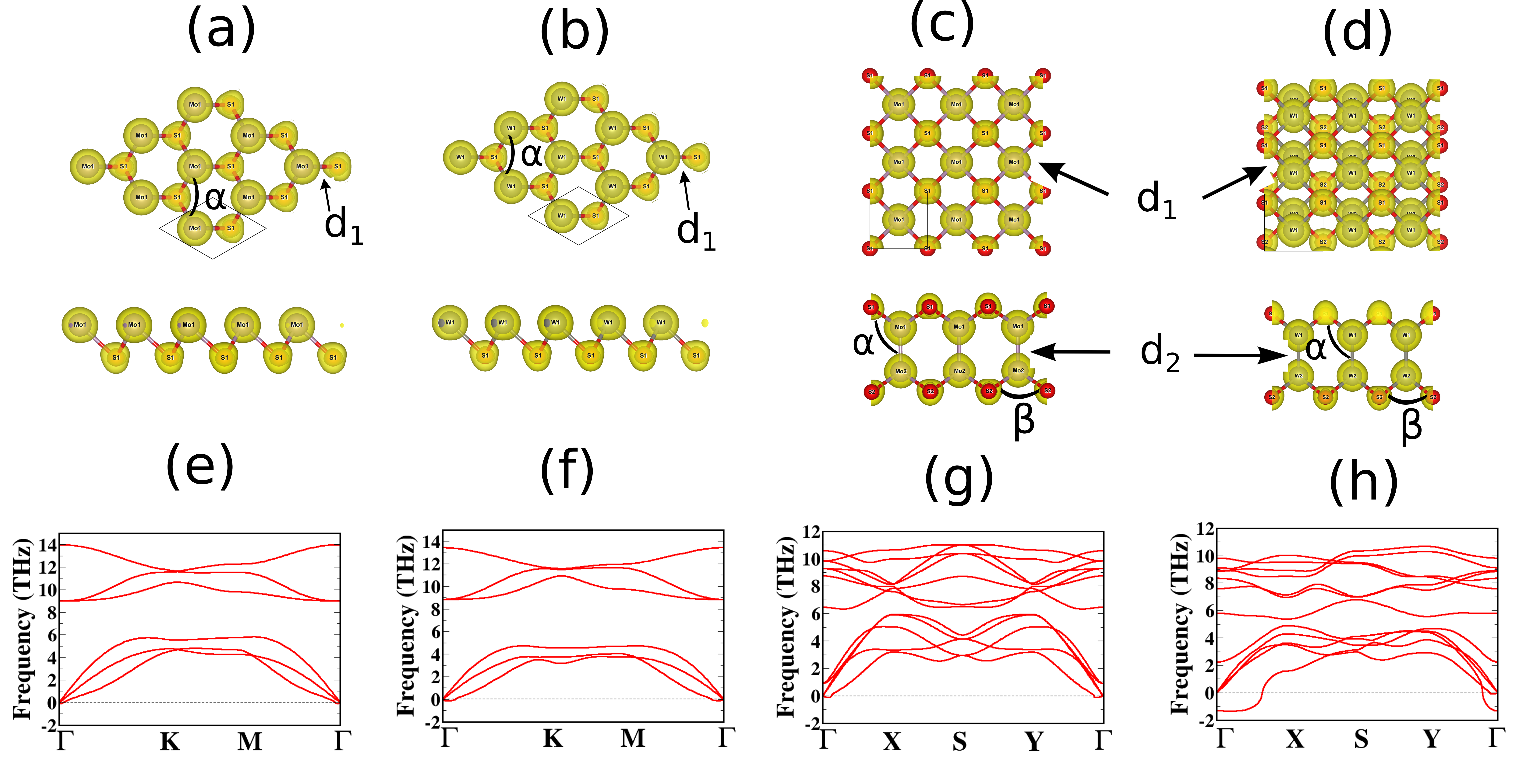
As mentioned above, we probe two configurations, buckled and puckered, for the MoS and WS monolayers. To check and compare the electronic stability of the structures, we calculate the binding energy per atom (/atom). From Table II, we note that for both, MoS and WS, puckered configuration is the lowest energy configuration. The difference between the two-configurations for MoS and WS are 0.51 and 0.43 eV/atom, respectively. Further, valence charge density distribution (VCDD) (Fig.1(a)-1(d))has been studied to predict the nature of bonding and the charge distribution in the system. From VCDD, it is clear that the charges are more localized on atoms which suggests that the nature of bonding is more ionic-like. We carried out analysis of Bader chargeBader which is expected to provide greater understanding of the bonding nature. It is to be noted that the Bader charge analysis corroborates with the findings of VCDD. Huge charge transfer is observed to occur between the X (= Mo, W) and S atoms for all the four monochalcogenides (Table II). The charge transfer is consistent with the difference in electronegativity of the atoms (as Mo and W has less electronegativity than S). Bader charge analysis also helps in explaining the relative stability of MoS and WS for the same configuration. From Table II, we note that, more charge transfer occurs in the WS system as compared to MoS system. Hence a stronger ionic-type bonding may lead to higher stability of WS systems. It is to noted that the same ionic-like nature is observed for Mo and W dichalcogenides.PhysicaB For example, in Mo, 0.90e is lost by Mo and each S gains 0.45e, PhysicaB , these values are close to those observed by us in case of MoS. To gain more insight into the nature of bonding, we carry out analysis of electron localization function (ELF), presented in the supplementary materialsupplementary which further supports the results obtained from VCDD and Bader charge analysis.
It is well known that vdW interaction, in spite of its weak strength, plays an important role in stabilizing several multi-layered systemsvdw-layered-sci-paper ; vdw1 ; vdw2 ; vdw3 . Probing the vdW interaction in the monolayers studied here can give us an insight about the interactions present in the systems. Therefore, vdW dispersion corrected calculations have been carried out for all the systems under study. Table II lists all the geometrical parameters (in the parantheses) obtained from the vdW corrected calculations as well. We observe that the lattice constants reduce in WS cases as a result of vdW forces acting on the atoms, indicating presence of a slightly stronger binding among the atoms in these systems. Further, it is noted that the energies of all the systems get slightly lowered (by a sub-eV range). This signifies that the vdW may only have a small contribution to the overall interaction present in these systems. The trend of the ordering of the configurations, in terms of energetics, however, remains unaltered. The rigidity and hence structural stability is also checked by analyzing the phonon-dispersion for all the systems under study. A brief discussion on the phonon modes for these systems will be discussed in the following section.
| Structure | /atom | , | , | |||
|---|---|---|---|---|---|---|
| MoS-buckled | -4.948949 | 3.000 | 1.577 | 2.342 | 79.6 | 0.50 |
| (-5.125175) | (3.000) | (1.577) | (2.342) | (79.6) | ||
| WS-buckled | -5.838209 | 2.976 | 1.617 | 2.658 | 78.18 | 0.55 |
| (-6.123231) | (2.962) | (1.618) | (2.354) | (77.9) | ||
| MoS-puckered | -5.461969 | 3.121 | - | 2.455, 2.356 | 116.1, 78.9 | 0.76 |
| (-5.729954) | (3.121) | (-) | (2.449, 2.325) | (115.6, 79.1) | ||
| WS-puckered | -6.266106 | 3.08, 3.01 | - | 2.448, 2.472 | 105.9, 77.9 | 0.78 |
| (-6.807773) | (3.014, 2.974) | (-) | (2.431, 2.443) | (107.2, 76.6) |
III.2 Phonon Dispersion
At T = 0K, a crystal lattice is in its ground state. Hence there is no contribution of phonons in the system. However, at a finite temperature, study of phonons is important as they play crucial role in governing the thermal and electrical properties of a material. Moreover, the stability of a structure is also dependent on its phonons modes. For a stable structure, all the phonon frequencies should be positive.phonon1 Here, we show the phonon dispersion along the high symmetry path (Fig.1(e)-1(h)) for all the four structures studied in this paper and comment on the structural stability of the systems.
Buckled cases: Since we know that there exist a total of 3N number of phonon modes, where N is the number of atoms in the unit cell of a system, six phonon modes are present in case of MoS and WS buckled configurations (as the number of atoms is two in these two cases). The lower three modes correspond to the acoustic and the other three to the optical modes. All the modes are having positive frequencies except one mode which has negligibly small value of imaginary frequency at the - point. This very small negative frequency may be considered as an effect of computational parameters as already observed in the literature.phonon ; arsenene For MoS-buckled case, there are three optical modes, in which two have values 9 THz (doubly degenerate) and one has a value of 14THz at -point. On the other hand, for WS-buckled case, the three optical modes are shifted slightly below as compared to the case of MoS.
Puckered cases: The puckered configuration for MoS and WS contain a total of 12 phonon modes. From Fig.1(h), we see that one of the phonon modes of WS has reasonably large imaginary frequency and thus this system is likely to lack the structural stability. The imaginary frequency can be attributed to the lower symmetry structure for puckered WS configuration. However, puckered MoS is found to have a stable structure as all the phonon modes are positive. Since puckered configuration for WS does not show structural stability, this system will not be considered for further discussion.
Regarding the possibility of growing 2D mono or dichalcogenide materials, we note that many techniques are available in the literature for fabricating these materials.review1 For example, fabrication of monolayer PtSe2 by direct selenization of Pt has been reported by Wang et al.PtSe2 Further, monolayer CuSe has also been grown using similar technique.CuSe Therefore, sulphidization on Mo and W metal substrates could be a probable method to grow the MoS and WS structures predicted in this study.
III.3 Electronic Structure
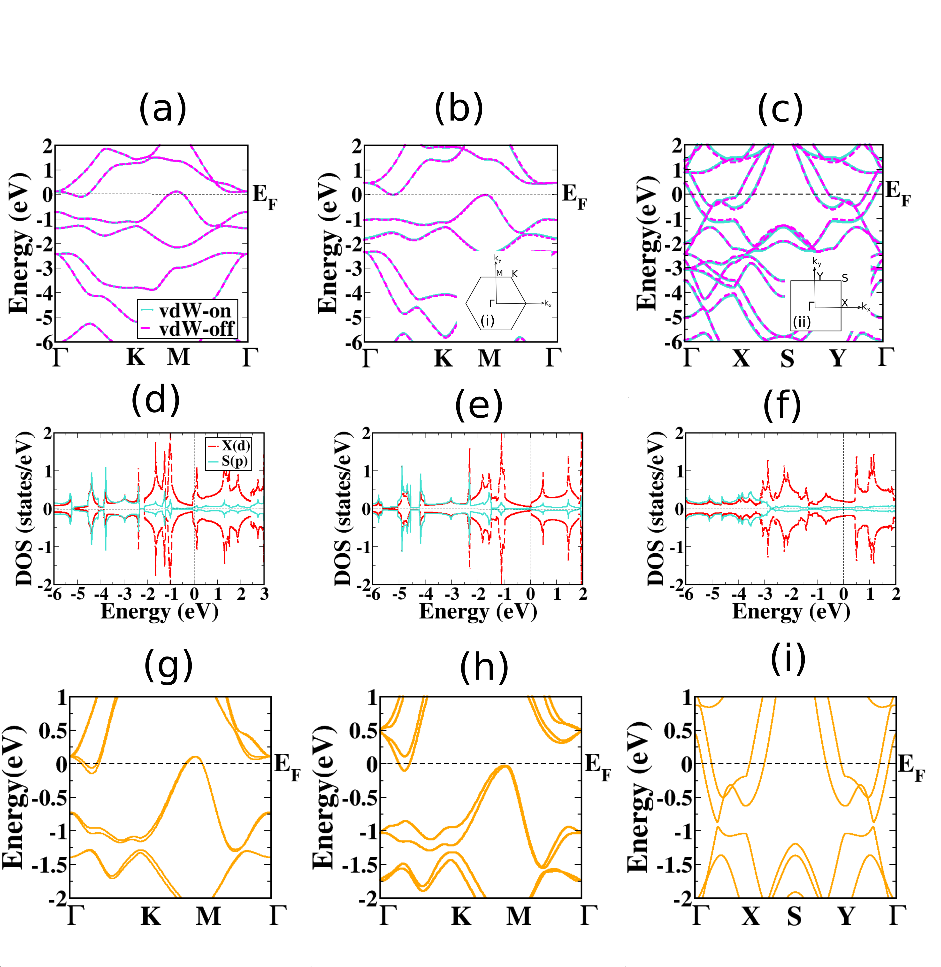
In this section, we present the results of electronic band structure and density of states (DOS) (Fig.2) for the monochalcogenide systems. We also analyze the partial DOS (PDOS) to understand the role of orbitals of different atoms in the system. We first discuss the results of the buckled-monochalcogenides followed by the puckered-cases.
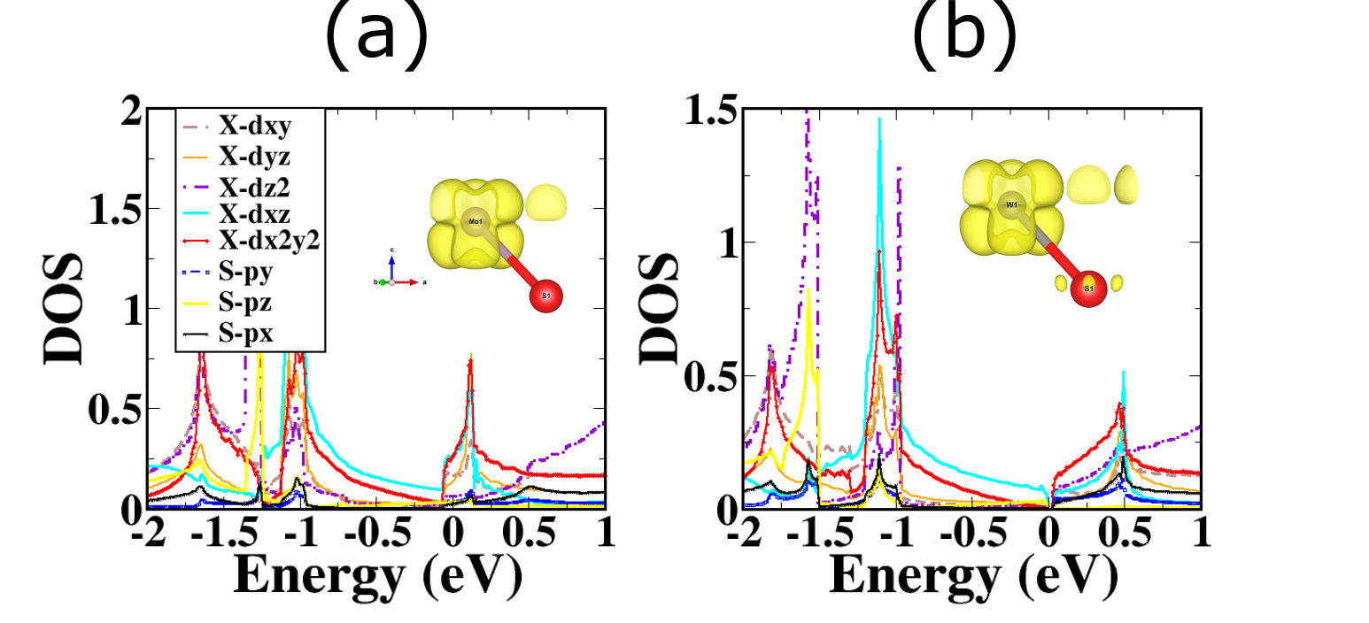
Buckled MoS is found to be a non-magnetic metallic system. It is apparent from the PDOS (Fig.2(a), 3(a)) that the Mo-d states has major contribution around Fermi energy () and hence the band edges comprise of Mo-d derived states with small contribution from S-p orbitals. However, below -2eV, Mo-d and S-p states are strongly hybridized. Fig.3 shows the orbital projected DOS with the partial charge density (PCD) (for C-point, i.e. the conduction band at the -point) for MoS. It is clear from Fig.3 that the bands in the region closer to the Fermi level has major contribution from and of Mo atom with very small contribution of S-p orbitals. PCD reveals the same nature of orbitals contributing to the DOS and bands slightly above the Fermi level.
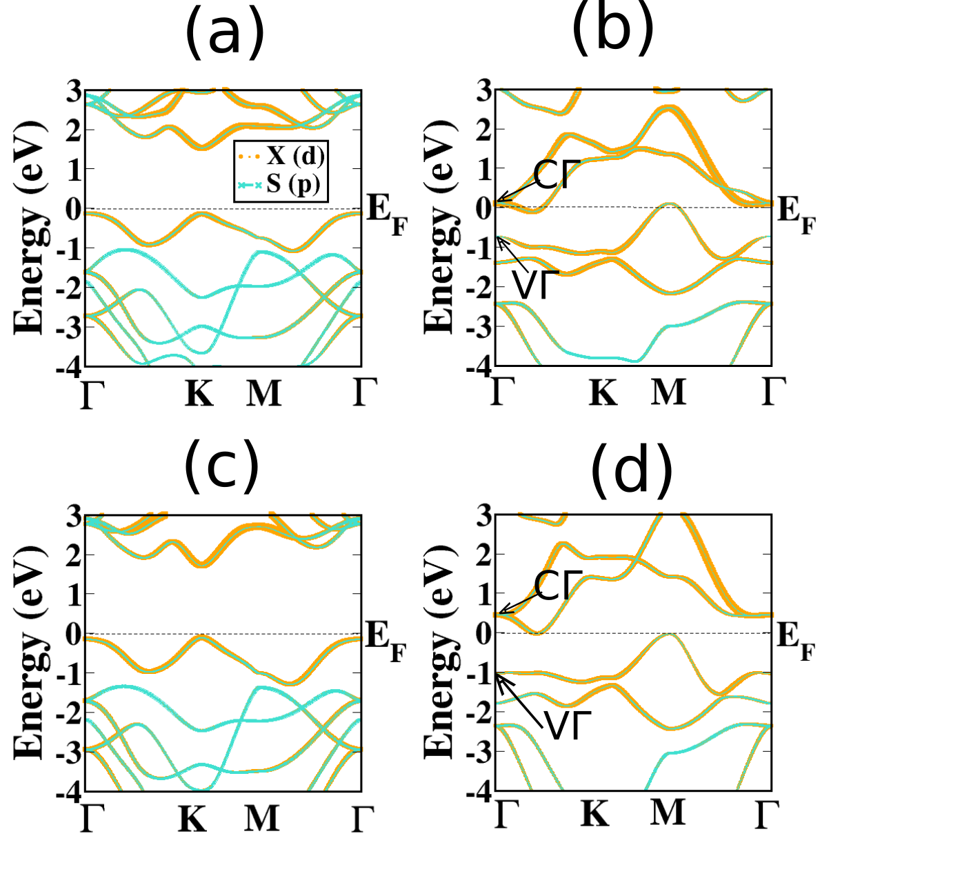
In the literature it is found that monolayer MoS2 and WS2 has a direct band-gap, in contrast to the corresponding monochalcogenide case.PhysicaB Therefore, we compare the two band structures, one of XS2 and XS where X is Mo and W as shown in Fig.4. It is to noted that the band gap obtained for MoS2 and WS2 are 1.65 eV and 1.84 eV respectively, which is consistent with the literaturePhysicaB . From the figure, we observe a band-gap in MoS2 which disappears in MoS. Moreover, the valence band maxima (VBM) and the conduction band minima (CBM) are at the same k-point for MoS2 which is not so in the MoS case. Further, we observe Mo-d bands in the conduction region closer to the Fermi level for MoS case compared to the corresponding dichalcogenide case. The clear difference in the electronic structure between the mono and dichalcogenides can be attributed to the absence of one S anion and hence the difference in hybridization between the cation and the anion in the MoS monochalcogenide system.
For the buckled WS case, the electronic structure calculation predicts a non-magnetic indirect-type semi-metallic nature for WS-buckled configuration as the VBM (which lies at the -point) and CBM lie at different k-points. Similar to the MoS-buckled case, the contribution to the DOS around is dominated by the W-d states and there is a stronger hybridization between W-d and S-p states farther below . However, unlike the corresponding MoS case, the d-states just above the Fermi-level have contribution from also the S-p orbitals along with the W-d states. This is justified by the respective PCD which in this case exhibits charge density around the S-atom as well. Similar to the comparative analysis of MoS2 and MoS, we observe a rearrangement of the bands in WS monochalcogenide case also. This leads to a change in the electronic nature due to the difference in W-S hybridization between the mono and dichalcogenides.
Effect of spin-orbit coupling (SOC) has also been probed as it may play an important role in modifying the electronic properties of the system as observed in the literature.SOC1 ; SOC11 ; SOC2 ; SOC3 ; SOC4 Wang et al. SOC3 have reported that WS2 used as a substrate opens a path for topological states of matter in graphene-based systems. It is well-known that SOC lifts the degeneracy of energy levels and hence causes the splitting of the levels. Fig.2(g)-2(i) shows the splitting of the electronic levels for the monochalcogenides. Furthermore, the inclusion of SOC changes the electronic structure of WS ( Fig.2(h)) such that we observe a slight splitting of the band corresponding to CBM along the -K path. The more appreciable effect of SOC in WS-buckled compared to the MoS case is expected as the spin-orbit interaction is more pronounced in the elements having higher atomic number.
For puckered MoS, the band structure and the DOS calculations reveal a non-magnetic metallic nature of the system with Mo-d electrons contributing to the states near . Effect of SOC on electronic structure has been probed and very small splitting is observed along -X and -Y path (as they are symmetric) and also at the S-point (at around -1.2 eV).
The band structures with van der Waals interaction are also plotted in Fig.2((a)-(c)), (dashed blue lines). It is observed that the vdW corrected band structures, are very similar in terms of the band dispersion and band energies when compared with the bands without vdW correction. Overall, it can be inferred that the vdW interaction is not likely to play a crucial role in these systems.
III.4 Band-gap engineering by application of strain
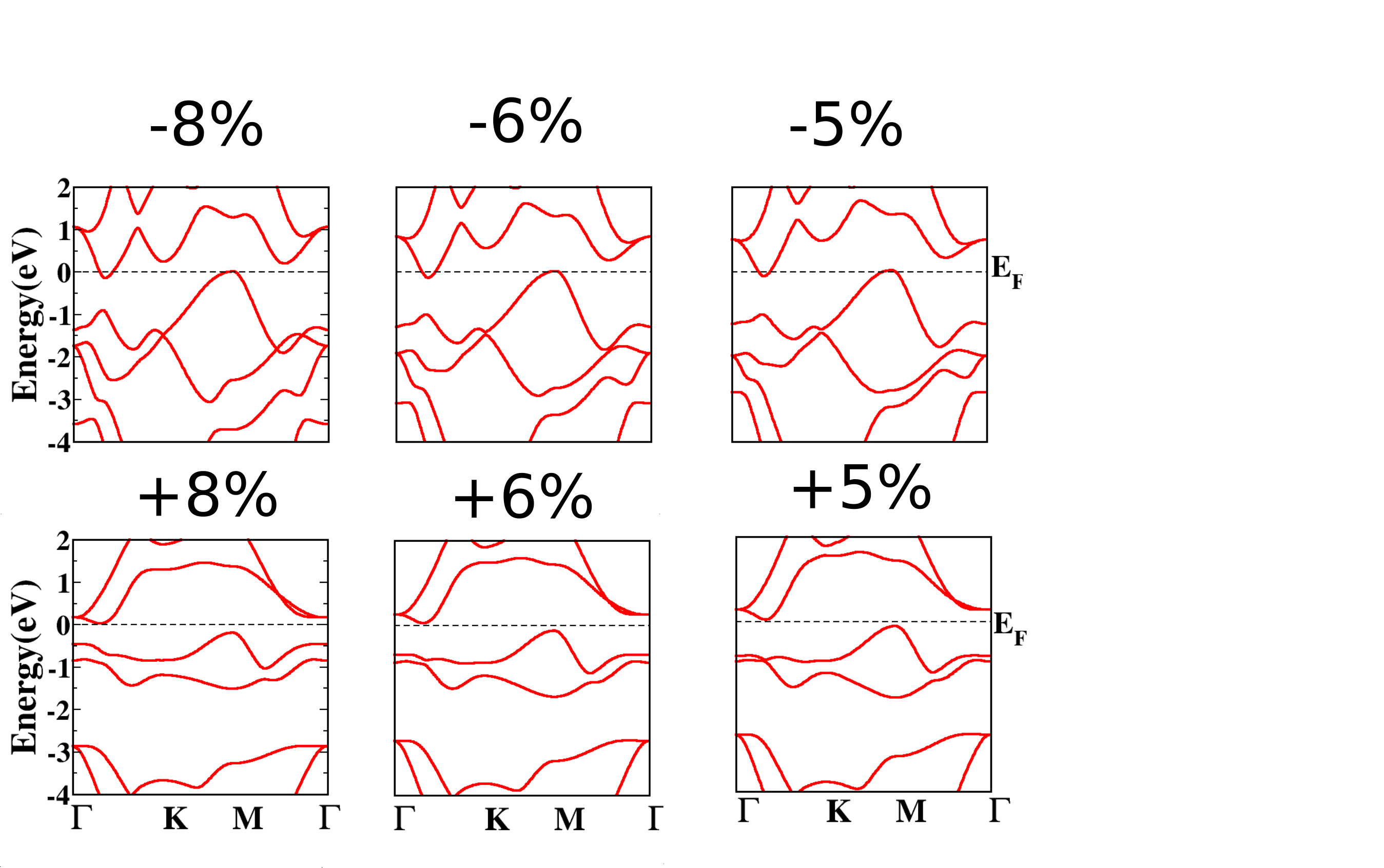
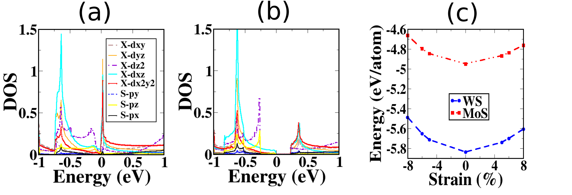
From the literature, it is observed that application of strain (tensile or compressive) plays a major role in the engineering of band-gaps in the material.PCCP12 ; ACSNano5SB ; NM8WW ; SSC227AEM ; strain1 ; strain2 ; strain3 Since WS buckled structure is found to be an indirect-type semi-metal, it may be interesting to probe its electronic structure after application of strain. The strain can be defined as = ((a-a0)/a0) 100%, where a and a0 are the lattice constants of strained and unstrained systems, respectively. For each value of bi-axial strain, all atoms are relaxed with the fixed lattice constant. We study the band evolution for both tensile as well as compressive bi-axial strain, with the amount of strain applied to be 5%, 6%, and 8%. In the bi-axial strain, we deform the in-plane lattice parameters and by an equal amount. The deformation obviously leads to changes in W-S distances, bond angles and the buckling parameter and hence in the electronic structure. From Fig.5, we observe that for the tensile bi-axial strain, a band-gap opens up. However, the band-gap obtained is found to be indirect. Occurrence of a gap is not observed for the compressive strain. The origin of the gap can be explained by the evolution of VBM (at -point) and CBM (along -K path). We observe that with the increase in the bi-axial tensile strain, the VBM at -point shifts below the level and the CBM (along -K path) shifts away from . The observed shifting of bands has the following origin. From Fig.2(b)and 2(e), it is apparent that the band edges comprise of predominantly the W-d states with a slight contribution from S-p states. The increase in tensile strain causes the lattice constant (therefore the W-W, W-S or S-S distances) (Table III) to increase. Consequently, the hybridization of W-d states and S-p states is decreased (Fig.7(b)) which leads to a gap. It is to be noted that C (0.46eV above the Fermi level) and V (at -1 eV) points are lowered and raised, respectively, towards the Fermi level with the increase in the tensile strain. However, +8% tensile strain is not sufficient to cause the Fermi level crossing of bands corresponding to -point and thus we observe an indirect semiconductor behavior of buckled WS monochalcogenide. On the other hand, if we observe the band evolution for the compressive strain, the reverse is observed. CBM and VBM crosses the Fermi level leading to a metallic state.
It is to be noted that unlike the WS case, for buckled MoS, application of strain does not show any metal-semiconductor transition. For the sake of comparison with the WS case, we discuss here the buckled MoS under tensile strain (Fig.6). Similar to the case of WS, the hybridization between Mo-d and S-p states is reduced (Fig.7(a)). The VBM is shifted below and the CBM shifts away from the Fermi level upward when tensile strain is applied to buckled MoS. However, along with this, the C (0.13 eV above the Fermi level) and V (at around -0.73 eV) (Fig.4) points also shift towards the Fermi level. In resemblance with the case of WS, C and V points move closer to on the application of a tensile strain. Since these two points are closer to as compared to that in WS case, it is apparent from Fig.7 that the shift of the bands at -point (i.e. C and V) towards the Fermi level is responsible for retaining the metallic behavior in this case.
It is worth-mentioning here that we have also calculated the binding energy per atom for the strained MoS and WS systems (Fig.7(c)). We find a parabolic behavior of energy as a function of the bi-axial strain. The unstrained system possesses the lowest energy. However, it is clear from Fig.5 that overall the tensile strained systems have comparatively higher binding energy (more negative) as compared to that of compressive strained systems. Thus from the energetics, it can be argued that the ease to stretch the system is more than to compress it.
Like silicon and germanium which are indirect band-gap semiconductors and used in the field of semiconductors, strain-applied indirect band-gap semiconductor buckled WS may be expected to find potential application in the semiconductor industry. However, though we arrive at an indirect semiconductor on application of tensile strain, it is to be noted that, the calculations have been performed at T = 0K. Effect of ambient conditions and the substrate effect can alter the electronic structure which requires further investigation and is beyond the scope of the present work.
| Strain (%) | a | ||||
|---|---|---|---|---|---|
| 5% | 3.124 | 1.556 | 2.382 | 81.9 | 0.14 |
| 6% | 3.154 | 1.545 | 2.388 | 82.7 | 0.17 |
| 8% | 3.213 | 1.520 | 2.40 | 84.1 | 0.20 |

IV Conclusion
Using density functional theory based ab initio calculations (VASP programme package), we predict two new monolayered monochalcogenides, namely, molybdenum monosulfide (MoS) and tungsten monosulfide (WS). We carry out full geometry optimization of two different configurations for the MoS and WS monolayer structures, buckled and puckered. From the structural and energetic stability point of view, we found that MoS is stable in both the configurations, the puckered being more stable. However, WS in puckered configuration, though energetically the most stable one, is found to be dynamically unstable. Further, effect of vdW has been studied which suggest negligible change in the electronic properties of the stable structures. VCDD and Bader charge analysis predicts an ionic-like bonding in the system. DOS and electronic band structure shows the non-magnetic metallic nature for MoS in both the stable configurations. On the other hand, for the buckled WS, our study reveals the non-magnetic indirect semi-metallic nature. The difference in the electronic nature of MoS and WS from their dichalcogenide analogue i.e. MoS2 and WS2 (which are both direct gap semiconductor) can be attributed to the absence of one sulphur atom and hence the difference in Mo(W)-S hybridization. Effect of spin-orbit coupling (SOC) has also been probed. It is observed that, since W has higher atomic number, the effect of SOC is slightly more pronounced in the case of WS, compared to MoS.
Finally, the effect of bi-axial tensile and compressive strain on the electronic structure has also been explored. Interestingly, a transition from semi-metal to an indirect band-gap semiconductor has been observed for the tensile strain of 5%, 6% and 8% in case of buckled WS. Thus, it is predicted that, with a suitable choice of a substrate, WS system may turn out to be important in the field of semiconductors.
V Acknowledgement
Authors thank P. A. Naik for facilities and encouragement. D.P. thanks C. Kamal for fruitful discussions. The scientific computing group, computer centre of RRCAT, Indore is thanked for the help in installing of and support in running the codes. D.P. thanks HBNI and RRCAT for financial support.
References
- (1) K. S. Novoselov, D. Jiang, F. Sehedin, T. J. Booth, V. V. Khotkevich, S. V. Morozov, A.K.Geim, Proc Natl Acad Sci U S A. 102,10451 (2005).
- (2) M. Chhowalla1, H. S. Shin, G. Eda, L.J. Li, K. P. Loh, H. Zhang, Nature Chemistry 5, 263 (2013).
- (3) E.S.Kadantsev , P. Hawrylak, Solid State Communications, 152, 909 (2012).
- (4) Y.Ding, Y.Wang, J.Ni, L.Shi, S.Shi, W.Tang, Physica B, 406, 2254 (2011).
- (5) S. Lebegue and O. Eriksson, Phys. Rev. B, 79, 115409 (2009).
- (6) C. Ataca, H. Sahin, E. Akturk and S. Ciraci, J. Phys. Chem. C, 115, 3934 (2011).
- (7) S. Bertalazzi, J. Brivio and A. Kis, ACS Nano, 5, 9703 (2011).
- (8) P.Lu, X.Wu, W.Guo, X.C.Zeng, Phys. Chem. Chem. Phys., 14, 13035 (2012)
- (9) Q. H. Wang, K. Kalantar-Zadeh, A. Kis, J. N. Coleman and M. S. Strano, Nat. Nanotech., 7, 699 (2012).
- (10) D. Jariwala, V. K. Sangwan, L. J. Lauhon, T. J. Marks and M. C. Hersam, ACS Nano, 8, 1102 (2014).
- (11) R. Ganatra and Q. Zhang, ACS Nano, 8, 4074 (2014).
- (12) J. Ryou, Y. -S. Kim, Santosh, K. C. and K. Cho, Sci. Rep., 6, 29184 (2016).
- (13) R. K. Defo, S. Fang, S. N. Shirodkar, G. A. Tritsaris, A. Dimoulas and E. Kaxiras, Phys. Rev. B, 94, 155310 (2016).
- (14) A. Oezden, F. Ay, C. Sevik and N. K. Perkgoez, Jap. J. Appl. Phys., 56, 06GG05 (2017).
- (15) W. Wang, C. Yang, L. Bai, M. Li and W. Li, Nanomaterials, 8, 74 (2018).
- (16) Th. Boeer, R. Severin, A. Mueller, C. Janowitz, R. Manzke, D. Voss, P. Krueger, A. Mazur and J. Pollmann, Phys. Rev. B, 64, 235305 (2001).
- (17) R. C. Cooper, C. Lee, C. A. Marianetti, X. Wei, J. Hone, J. W. Kysar, Phys. Rev. B, 87, 035423 (2013).
- (18) K. F. Mak, C. Lee, J. Hone, J. Shan and T. F. Heinx, Phys. Rev. Lett., 105, 136805 (2010); S. W. Han, H. Kwon, S. K. Kim, S. Ryu, W. S. Yun, D. H. Kim, J. H. Hwang, J. -S. Kang, J. Baik, H. J. Shin and S. C. Hong, Phys. Rev. B, 84, 045409 (2011).
- (19) E. Scalise, M. Houssa, G. Pourtis, V. V. Afanasev and A. Stesmans, Physica E, 56, 416 (2014).
- (20) B. Radisavljevic, A. Radenovic, J. Brivio, V. Giacometti and A. Kis, Nat. Nanotech., 6, 147 (2011); H. Liu and P. D. Ye, IEEE ELect. Dev. Lett., 33, 546 (2012).
- (21) K. C. Santosh, R. C. Longo, R. Addou, R. M. Wallace and K. Cho, Nanotechnology, 25, 375703 (2014).
- (22) A. E. Maniadaki, G. Kopidakis and I. N. Remediakis, Solid State Comm., 227, 33 (2016).
- (23) W. S. Yun, S. W. Han, S. C. Hong, I. G. Kim and J. D. Lee, Phys. Rev. B, 85, 033305 (2012); R. Bhandavat, L. David and G. Singh, J. Phys. Chem. Lett., 3, 1523 (2012); R. H. Gutierrez, N. Perea-Lopez, A. L. Elias. A. Berkdemir. W. Bei, R. Lv, F. Lopez-Urias, V. H. Crespi, H. Terrones and M. Terrones, Nano Lett., 13, 3447 (2013); A. Berkdemir, H. R. Gutierrez, A. R. Botello-Mendez, N. Perea-Lopez, A. L. Elias, C. -I. Chia, B. Wang, V. H. Crespi, F. Lopez-Urias, J. -C. Charlier, H. Terrones and M. Terrones, Sci. Rep., 3, 1755 (2013); F. Lan, R. Yang, Y. Xu, S. Qian, S. Zhang, H. Cheng and Y. Zhang, Nanomaterials, 8, 100 (2018).
- (24) C. Kamal, Aparna Chakrabarti, M. Ezawa, Phys. Rev. B, 93, 125428 (2016).
- (25) L.Xu, M.Yang, S.J.Wang, Y.P.Feng, Phys Rev B 95, 235434 (2017)
- (26) A.K.Singh, R.G Hennig, Appl. Phys. Lett. 105, 042103 (2014)
- (27) F.Wang, L.Zhou, Z.Ma , M. He, F. Wu, Y. Liu, Nanomaterials 8, 789 (2018).
- (28) M. Yagmurcukardes, R.T.Senger, F. M. Peeters, H. Sahin, Phys Rev B 94, 245407 (2016).
- (29) Z.Q.Huang, W.C.Chen, G.M.Macam, C.P.Crisostomo, S.M.Huang, R.B.Chen, M.A.Albao, D.J.Jang, H.Lin, F.C.Chuang, Nanoscale Research Letters 13, 43 (2018).
- (30) B.P. Bahuguna, L.K. Saini, R.O.Sharma, Brajesh Tiwari, Physica E: Low-dimensional Systems and Nanostructures 99, 236 (2018).
- (31) A. Shafique, Y.H.Shin, Scientific Reports 7, 506 (2017).
- (32) See Supplemental Material for details.
- (33) G. Kresse, J. Furthmüller, Phys. Rev. B, 54, 11169 (1996); G. Kresse, D. Joubert, Phys. Rev. B, 59, 1758 (1999).
- (34) P. E. Blöchl, Phys. Rev. B, 50, 17953 (1994).
- (35) J. P. Perdew, K. Burke, M. Ernzerhof, Phys. Rev. Lett., 77, 3865 (1996).
- (36) A. Togo, Phonopy, http://phonopy.sourceforge.net/
- (37) S. Grimme, J. Comp. Chem. 27, 1787 (2006).
- (38) G. Henkelman, A. Arnaldsson, H. Jonsson , Comp. Mater. Sci., 36, 36254 (2006).
- (39) D.L.Duong, S.J.Yun, Y.H.Lee, ACS Nano 11, 11803(2017)
- (40) K.Liu, L. Zhang, T. Cao, C.Jin, D. Qiu, Q. Zhou, A. Zettl, P. Yang, S. G. Louie, F. Wang, Nat. Commun. 5, 4966 (2014).
- (41) Lee, C.; Yan, H.; Brus, L. E.; Heinz, T. F.; Hone, J.; Ryu, S. ACS Nano, 4, 2695 (2010)
- (42) S. Wang, H. Tian, C. Ren, J. Yu, M. Sun, Sci Rep. 8, 12009(2018).
- (43) G. Grimvall, B. Magyari-Köpe, V. Ozoliņš, K. A. Persson Rev. Mod. Phys. 84, 945 (2012).
- (44) H. Sahin, S. Cahangirov, M. Topsakal, E. Bekaroglu,E. Akturk, R. T. Senger, and S. Ciraci, Phys. Rev. B 80, 155453(2009).
- (45) C. Kamal, M. Ezawa, Phys. Rev B 91, 085423 (2015).
- (46) G. Li, Y.Y.Zhang, H.Guo, L. Huang, H. Lu, X.Lin, Y.L.Wang, S.Du, H.J.Gao, Chem.Soc.Rev. 47, 6073 (2018).
- (47) Y. L. Wang, L. F. Li, W. Yao, S. R. Song, J. T. Sun, J. B. Pan, X. Ren, C. Li, E. Okunishi, Y. Q. Wang, E. Y. Wang, Y. Shao, Y. Y. Zhang, H. T. Yang, E. F. Schwier, H. Iwasawa, K. Shimada, M. Taniguchi, Z. H. Cheng, S. Y. Zhou, S. X. Du, S. J. Pennycook, S. T. Pantelides and H. J. Gao, Nano Lett. 15 , 4013 (2015).
- (48) L.Gao, J.T.Sun, J.C.Lu, H.Li, K.Qian, S.Zhang, Y.Y.Zhang, T.Qian, H.Ding, X.Lin, S.Du, H.J.Gao, Adv. Mater. 30, 1707055 (2018).
- (49) M. Gmitra, S. Konschuh, C. Ertler, C. Ambrosch-Draxl, J. Fabian, Phys. Rev. B 80, 235431 (2009).
- (50) Chen-Huan Wu, arXiv:1804.01695 [cond-mat.mtrl-sci]
- (51) M. Gmitra and J. Fabian, Phys. Rev. B 92, 155403 (2015).
- (52) Z. Wang, Dong–Keun Ki, H. Chen, H. Berger, A. H. MacDonald, A. F. Morpurgo Nature Communications 6, 8339 (2015).
- (53) Sergio et al., Nature Communications 9,1427(2018).
- (54) X. Peng, Q.Wei,A.Copple,Phys. Rev. B 90, 085402 (2014).
- (55) A. S. Rodin, A. Carvalho, and A. H. Castro Neto, Phys. Rev.Lett. 112, 176801 (2014).
- (56) H. Liu, A. T. Neal, Z. Zhu, X. Xu, D. Tomanek, and P. D. Ye, ACS Nano 8, 4033 (2014).