Advanced Digital Signal Processing Techniques for High-Speed Optical Communications Links
keywords:
pdfLaTeX LuaLaTeX XeLaTeX PhD doctoral programs PhD dissertation Politecnico di TorinoCapitolo 1 Introduction
In the past 20 years, the total world Internet traffic has grown by an enormous rate () [Winzer:2018]. To sustain this growth, all components of the Internet infrastructure have steadily evolved. Focusing on the raw speed of point-to-point optical links, it is interesting to see the compound annual growth rate [Winzer:2017, Fig. 4] of the per- interface rate and its relative symbol rate. While the interface rate has experienced a annual growth rate, the symbol rates have grown by just . This means that, to sustain this growth, also the spectral efficiency had to steadily evolve.
Among the different technological improvements, the introduction of Digital Signal Processing (DSP) techniques, initially taken from the wireless communications community, has given a tremendous boost to spectral efficiency. This has been possible thanks to the improvements in the speed of CMOS circuits [Winzer:2018, Sec. 2.3]. The first DSP application in optical communications was on high-speed long-haul links. In this scenario, DSP enabled coherent detection and polarization multiplexing, allowing a dramatic increase in spectral efficiency. More recently, DSP has been also applied to shorter links, such as inter data-center communications, or even intra data-center links [Zhong:2018]. Therefore, introduction of DSP in optical communications have been one of the key technological improvements that allowed such speed increase.
Consequently, the purpose of this thesis is to investigate the application of DSP to different optical communications applications, from short-reach ( km) data-center interconnects, to long-haul links. These links can be divided into two large categories, based on the receiver structure: direct-detection and coherent detection. Indeed, the structure, the requirements, and (most importantly) the DSP algorithms radically differ in these categories.
For this reason, this thesis is divided into two Parts. Part I is devoted to direct-detection systems. After an introduction in Chapter 2, Chapter 3 will present a novel DSP-enabled architecture for km links, while Chapter 4 will focus on km inter data-center links. Part LABEL:part:coh will be instead devoted to coherent systems. In particular, it will be focused on the application of the constellation shaping DSP technique to long-haul links. After an introduction in Chapter LABEL:ch:coherent, Chapter LABEL:ch:shaping will be focused on constellation shaping on an Additive White Gaussian Noise (AWGN) channel, while Chapter LABEL:ch:phnoise will instead focus on the generation (and compensation) of non-linear phase noise by fiber non-linear effects.
Parte I Direct-Detection Systems
Capitolo 2 Introduction to Direct-Detection Systems
This Chapter introduces direct-detection systems, which are widely-adopted in short reach ( km) links, typically present in data-centers (DC). After a general introduction to DC networking, presenting the most common standards, attention will be focused on two different scenarios: connections within a DC (Intra-DC) and between different DC (Inter-DC).
Afterwards, two Chapters (3 and 4) will present the contribution of this thesis to these topics, presenting a novel spatial-multiplexing architecture for Intra-DC (Chapter 3) and a comparison between intensity modulation and single-sideband transmission for Inter-DC (Chapter 4).
2.1 Introduction
During past decade, research in high-speed optical communications was focused on long-distance links, which used to be the network segment where traffic was steadily growing [Desurvire:2006]. This lead to the development of coherent transmission and detection schemes, which were able to dramatically increase network capacity. At that time, almost all short distance links employed simple NRZ intensity modulation / direct-detection at relatively low data-rates [std:ethernet2002], with very simple (if any) digital signal processing involved.
Nowadays, new applications such as cloud computing, video-on-demand, virtual and augmented reality demand a large capacity increase on links in the DC [Cheng:2018]. According to [CiscoGCI:2018, Appendix B], in 2021 93.9% of the total IP traffic on the Internet will be between end users and DC. Moreover, this traffic accounts only for 14.9% of the total DC-related traffic, while the rest will be between DC (13.6%) and inside each DC (71.5%). Therefore, more sophisticated architectures, modulation formats and signal processing are required to cope with this traffic increase.
In this particular scenario, there are challenges that are quite unique in the field of optical communications [Zhong:2018]. As opposed to long-distance links, single interface data-rate is only one of the factors that needs to be improved. Other elements, such as cost, form factor, power consumption and latency are extremely important for this scenario, and they need to be carefully taken into account when developing new algorithms and architectures for short-reach applications.
In this Chapter, it will be given an overview of current standard and interfaces for short-reach direct-detections applications, focusing on the DC environment, which can be divided into two main groups:
-
•
Intra-DC: connections inside a data-center, usually shorter than km.
-
•
Inter-DC: connections between different data-centers in a region, in the range of km. This application can also be called Data-Center Interconnect (DCI).
Solutions adopted for these two groups are quite different. Intra-DC links, given the limited distance, do not need optical amplification, therefore they can transmit in the O-band and avoid chromatic dispersion. Inter-DC links, instead, require optical amplifications, forcing the use of C-band and thus facing the problem of chromatic dispersion. Because of this, current (and future) solutions for these applications will radically differ. Consequently, this Chapter will be divided into two Sections: 2.2, and 2.3, dealing (respectively) with Intra-DC and Inter-DC links.
2.2 Intra-DC links
2.2.1 Ethernet standards and form factors
[b]0.48
 {subfigure}[t]0.48
Inside the DC, most links are based on well-defined standards. The most common standards are Ethernet111https://ethernetalliance.org/, Fibre Channel222https://fibrechannel.org/ and InfiniBand333https://www.infinibandta.org/. In general, the main difference between these standards is the application: InfiniBand is mainly adopted for high-performance computing, Fibre Channel for storage and Ethernet for IP traffic. However, the differences primarily lay at higher networking layers, while in the physical layer the standards are similar.
Recently, adoption of Ethernet has been steadily growing, even outside its standard use cases. Since a study of the networking aspects of these standards is out of the scope of this thesis, we will choose Ethernet as a reference standard, keeping in mind that the physical layer differences with the other standards are small.
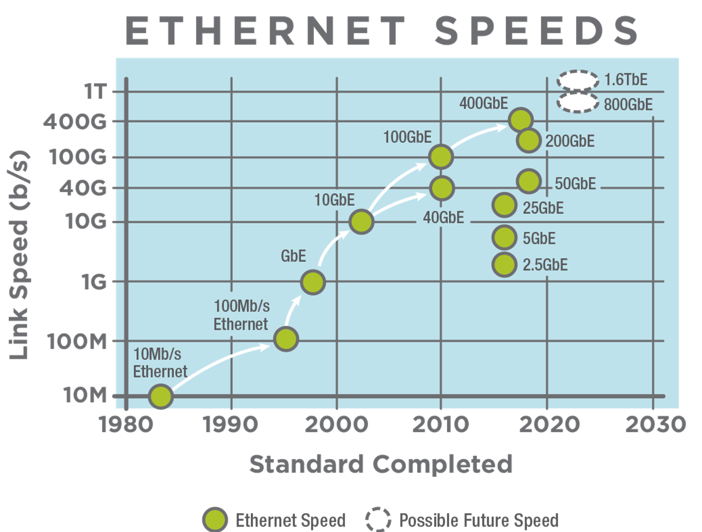
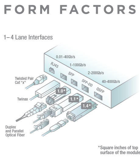
Fig. 2.3 shows the evolution, over the years, of the data-rates of the Ethernet standards. The oldest standard, released in 1983, used a single copper coaxial cable at a data-rate of 10 Mbit/s. Since then, line-rate increased exponentially, up to the most recent standard of 400 Gbit/s, released at the end of 2017. At the same time, technology improvements were able to reduce the form factor (hence, power consumption) of the transceiver. For instance, the first 100GBASE-LR4 interfaces, which achieve a data-rate of 100 Gbit/s over 10 km of Single-Mode Fiber (SMF), used the CFP form factor, whose size is mm and maximum power consumption W[Cisco:100GBASECFP]. Modern 100GBASE-LR4 transceivers use the QSFP28 form factor, whose size is mm, with a power consumption of W[Cisco:100GBASEQSFP].
Transceivers are usually pluggable with standardized form factors. Current form factors of modern Ethernet standards are shown in Fig. 2.3. At speed lower (or equal) than 1 Gbit/s, interfaces mainly use copper twisted-pair cables with the RJ-45 corrector. Above 1 Gbit/s, and up to 100 Gbit/s, different variants of the SFP form factor are used. Then, for higher-speed interfaces, the SFP-DD444http://sfp-dd.com/ and QSFP-DD555http://www.qsfp-dd.com/ form factors are used, which are slightly larger (and consume more power) than SFP.
400-Gbit/s Ethernet
At the time of writing this thesis, the highest-speed published Ethernet standard is IEEE 802.3bs-2017 [std:ethernet2017], released in 2017, which defines several standards at 200 Gbit/s (200GBASE) and 400 Gbit/s (400GBASE), which will be analyzed in the following Section.
| \topruleName | Medium | WDM | Symbol rate | Modulation | Reach |
| channels | (GBaud) | format | (km) | ||
| \midrule400GBASE-SR16 | MMF | 1 | 26.5625 | NRZ | 0.1 |
| 400GBASE-DR4 | SMF | 1 | 53.125 | PAM-4 | 0.5 |
| 400GBASE-FR8 | SMF | 8 | 26.5625 | PAM-4 | 2 |
| 400GBASE-LR8 | SMF | 8 | 26.5625 | PAM-4 | 10 |
| \bottomrule |
Focusing on the 400 Gbit/s standards, 802.3bs defines different physical layer specifications over optical fiber, depending on the distance, which are summarized in Table 2.1. Moreover, the list of 400GBASE standards is quickly evolving, and new standards are expected to be released in the future. All the standards use parallel channels to obtain 400 Gbit/s, either using multiple media (SR16 and DR4) or WDM (FR8 and LR8). Except for SR16, the PAM-4 modulation format is used to increase spectral efficiency and reduce the number of parallel lines. Still, longer-distance standards require 8 parallel paths, which represents a significant source of complexity and cost.
From a signal-processing perspective, the most challenging standards are longer-reach ones (FR8 and LR8), since they have to deal with tighter power budgets. From an architectural point of view, the two standards are identical, except from the power budget (for details, we refer the reader to [std:ethernet2017]).
A basic block scheme of FR8/LR8 standards is shown in Fig. 2.4. The line speed of 400 Gbit/s is achieved using 8 parallel WDM channels, each using the PAM-4 modulation format at 50 Gbit/s. Channels are spaced by 800 GHz in the O-band, and each channel has a bandwidth of approximately 367.7 GHz to allow some tolerance in the laser wavelength. Channel central frequencies are taken from the 100-GHz DWDM grid [std:dwdm]. The central freqiencies (and wavelengths) of this grid are shown in Table 2.2; this grid is also called LAN-WDM (or LWDM) grid.

| \topruleChannel | Frequency | Wavelength |
|---|---|---|
| (THz) | (nm) | |
| \midrule1 | 235.4 | 1273.54 |
| 2 | 234.6 | 1277.89 |
| 3 | 233.8 | 1282.26 |
| 4 | 233.0 | 1286.66 |
| 5 | 231.4 | 1295.56 |
| 6 | 230.6 | 1300.05 |
| 7 | 229.8 | 1304.58 |
| 8 | 229.0 | 1309.14 |
| \bottomrule |
Forward Error Correction
The choice of a proper FEC algorithm for this application is not trivial, since it must combine high performance with low latency, power consumption and silicon footprint. For these reasons, soft-decision FEC, widely deployed in long-haul links, is not adopted, relying instead on simpler hard-decision FEC.
For 100 Gbit/s Ethernet, the IEEE has standardized two different FEC codes, KR4 and KP4. KR4 is a Reed-Solomon RS(528,514) code, specifically targeted for NRZ modulation, while KP4 is a more powerful RS(544,514), and it is targeted for PAM-4 modulation. For 400 Gbit/s, the IEEE adopted the KP4 code.
This code achieves a post-FEC BER of with a pre-FEC BER of approximately , with an electrical coding gain of dB [techrep:400gfec]. More details on FEC for short-reach applications can be found in [phd:shoaib, Chapter 6].
2.2.2 Channel model
For these applications, fiber channel model is quite unique, given the use of intensity modulation/direct detection and the very short propagation distances involved. The most important difference with respect to longer-distance communications is the use of O-band ( nm) instead of the popular C-band ( nm), which means that the attenuation and chromatic dispersion profiles will be different.
In this Section, the main characteristics of the channels are summarized, focusing on the differences with respect to C-band.
Chromatic dispersion
The main reason for the use of O-band is the low value of chromatic dispersion, which allows avoiding the need of dispersion compensation, at least at the symbol rates of interest.
However, even if the value of chromatic dispersion is low, it is not zero, and it may affect transmission at high symbol rates. For single-mode fiber, the range of chromatic dispersion is defined by ITU-T recommendation G.652 [std:smf]. As an example, in Fig. 2.5 it is shown the dispersion range of a G.652.B SMF fiber in the O-band, obtained using [std:smf, eq. (6-1)].
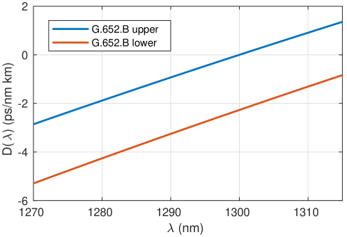
For the 400GBASE-FR8 standard (2 km SMF), the first WDM channel (with central wavelength nm) experiences the strongest chromatic dispersion, which in the worst case can be ps/nm. In [Eiselt:2016], the authors measured the CD tolerance of a -GBaud PAM-4 signal, and found dB penalty with ps/nm of dispersion. Therefore, we can conclude in this scenario dispersion can be completely neglected.
Attenuation
In the O-band, fiber attenuation is slightly higher than C-band. According to G.652 recommendation, attenuation in the O-band must be lower than dB/km, while in the C-band must be lower than dB/km. Modern SMF fibers have smaller values. For instance, measurements of a modern (G.652.D) SMF fiber performed in our lab found an attenuation of dB/km at nm and dB/km at nm.
Nevertheless, given the limited propagation distance ( km for all 400 Gbit/s standards), propagation loss represents a small contribution to the overall link budget. For instance, the total link power budget for 400GBASE-FR8 ( km SMF) is dB, and fiber propagation accounts only for dB (which assumes dB/km attenuation).
Polarization Mode Dispersion
According to G.625 recommendation, the maximum value of PMD is , even if modern SMF fibers have smaller values [Breuer:2003].
Nevertheless, in [Eiselt:2016] the authors measured a -dB penalty in -GBaud PAM-4 for DGD values greater than ps, which is not realistic for the distances of interest. Therefore, we conclude that also PMD can be neglected in this scenario.
Noise
Since optical amplification is not employed, the main source of noise is receiver thermal noise. For this thesis, laser relative intensity noise (RIN), which can be a significant noise source, especially for Directly-Modulated Lasers (DMLs) is neglected. Regarding thermal noise, the performance metric is the Received Optical Power (ROP). The variance (in current) of noise can be evaluated from the equivalent-input noise power spectral density , reported on receivers datasheets, with
| (2.1) |
where the electrical bandwidth of the receiver.
2.2.3 Modulation formats and signal processing
Intra-DC systems use simple intensity modulation, which, in the optics domain, basically means using Pulse Amplitude Modulation (PAM). Since legacy NRZ-OOK is equivalent to PAM-2, this Section will only deal with PAM- modulation without any loss of generality.
Pulse Amplitude Modulation

With PAM-, the transmitter encodes bits in different amplitude levels, where is a power of two, and the number of transmitted bits per symbol. Fig. 2.6 shows an example of PAM- levels, ranging from the first level to the last . From this definition, the average transmit optical power is trivial to evaluate
| (2.2) |
However, optical power does not fully characterize the system, because the Bit Error Ratio (BER) depends on the relative spacing between levels. Therefore, the Ethernet standards use another parameter, called outer Optical Modulation Amplitude (OMA), defined as the difference (in linear scale) between the lowermost and uppermost levels:
| (2.3) |
This parameter is linked to the average optical power by means of another parameter, called Extinction Ratio (ER), defined as the ratio between the lowermost and uppermost levels . Assuming equispaced levels, the relation is
| (2.4) |
Bit Error Ratio of PAM
Using the definition of outer OMA and PAM detection theory [proakis2007digital, Ch. 4], the Symbol Error Ratio (SER) of an IM/DD PAM system limited by electrical receiver noise can be evaluated from the distance between the equispaced levels:
| (2.5) |
By substituting this definition into the expression of the Symbol Error Ratio of PAM, the SER can be calculated as:
| (2.6) |
where is the photodiode responsitivity (expressed in A/W). Note that, in this expression, the argument of the erfc function is directly proportional to the received optical power.
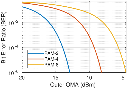
Fig. 2.7 shows an example of BER (assuming Gray mapping) as a function of the outer OMA for -GBaud PAM transmission. Photodiode responsivity was set to A/W and noise current to . Asymptotically, a one-bit increase in the modulation format requires a dB increase of the OMA.
Digital Signal Processing
IM/DD systems are inherently very simple, and they are used to operate without any DSP algorithm. However, with the increase of symbol rate and multilevel modulation, limited bandwidth of components starts to become an issue, requiring some sort of channel equalization at the receiver.
In literature, there have been presented several equalization techniques [Zhong:2018]. Some of them, such as Maximum Likelihood Sequence Estimator (MLSE) are able to dramatically improve transmission in presence of strong bandwidth limitations, but its complexity may be overkill for Intra-DC applications.
To have an overview of the current commercial state-of-the-art, the Ethernet standard uses a -tap T-spaced feed-forward equalizer (FFE) for testing the Transmitter and Dispersion Eye Closure Quaternary (TDECQ) of 400GBASE-FR8 and LR8 standards. For the implementation of the actual receiver, the IEEE does not give any recommendation. In presence of strong bandwidth limitations, non-linear Decision Feedback Equalizers (DFE) are commonly employed [Zhong:2018].
2.3 Inter-DC connections
Modern data-centers are based on distributed architectures, where there are several DC inside the same region to provide scalability and redundancy [Nagarajan:2018]. This architecture represents a radical change with respect to the traditional “mega data-center” approach, and it has driven market demand to high-speed connectivity between those DC. Since this Inter-DC scenario is more similar to the long-haul scenario, standard coherent line-cards may be adopted to deliver the required capacity. However, Inter-DC connections have stricter requirements in term of latency, cost and power consumption which makes coherent long-haul systems unfeasible.
In this scenario, as opposed to Intra-DC, there are not well-defined standards. This, on one hand, gives more freedom to the system designer. On the other hand, it makes it difficult to retrieve the technical specifications of current Inter-DC systems. Therefore, this Section will be devoted to the channel model and a brief comparison of the proposed modulation techniques.
2.3.1 Channel model
As a generally accepted definition, Inter-DC encompasses links between and km. However, links that are shorter than km can be treated as “long” Intra-DC links, since they can employ the same modulation formats and architectures as Intra-DC. For longer distances, link budget become too tight, requiring optical amplification and moving the transmission wavelengths to the C-band. This means that some forms of dispersion compensation are necessary.
The use of optical amplification changes the type of noise that is impairing an Inter-DC link. While Intra-DC links are mainly limited by receiver thermal noise, optically-amplified Inter-DC links are limited by ASE noise inserted by the amplifiers. Therefore, the main performance metric becomes the OSNR, defined as power of the signal (in two polarizations) divided by the power of ASE. Consequently, this scenario becomes similar to a long-haul transmission system. The main difference is PMD, which, as for the same reasons explained in Sec. 2.2.2, can be neglected.
2.3.2 Coherent vs. intensity modulation
Given the channel model, for Inter-DC both coherent and IM/DD systems can be adopted. The goal of this Section is to perform a comparison on the key differences between the two schemes, focusing on Inter-DC applications. Part of this Section has been presented at ICTON 2018 conference as an invited presentation [Pilori:ICTON2018].
[b].45
 {subfigure}[b].45
 {subfigure}[b].45
 {subfigure}[b].45
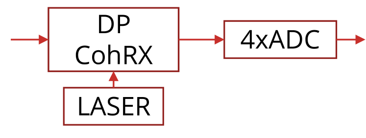
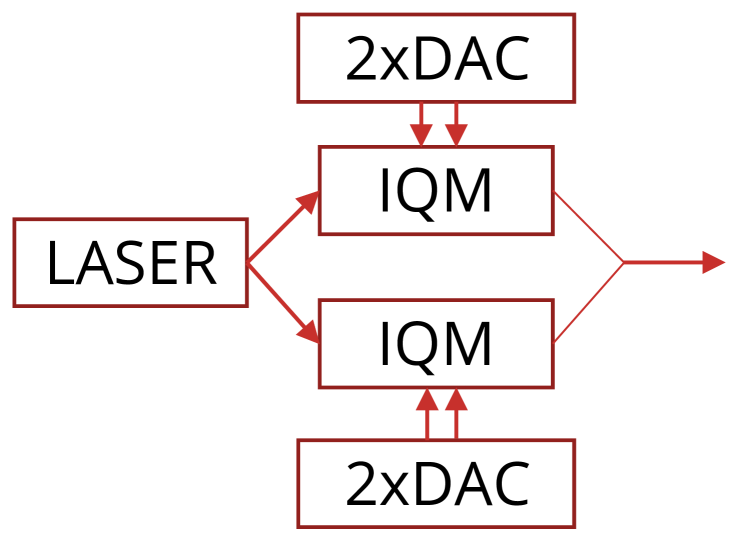
A high-level comparison between IM/DD systems and coherent architectures is shown on Fig. 2.12. Starting with the transmitter, an IM/DD transmitter (Fig. 2.12), other than a laser, only needs an intensity modulator, which can be either a Mach-Zehnder Modulator (MZM) or an Electro-Absorption Modulator (EAM). In some cases, the laser is even directly modulated. The electrical signal is generated by a DAC with a small bit resolution, since pulse-shaping is generally not applied. A coherent system, instead, (Fig. 2.12), needs a low-linewidth laser, a dual-polarization I/Q MZM, four DACs with high-enough resolution to apply pulse shaping. At the receiver, while an IM/DD receiver (Fig. 2.12) just needs a photodiode followed by an ADC, a coherent receiver (Fig. 2.12) needs a laser, a dual-polarization coherent receiver, which includes two hybrids and balanced photodetectors, and ADCs.
| \toprule | PAM- (IM/DD) | PM--QAM (coherent) |
|---|---|---|
| \midruleDispersion compensation | Optical | Electrical |
| Spectral efficiency | (bit/s/Hz) | (bit/s/Hz) |
| \bottomrule |
By looking at the architecture, complexity and thus cost of a coherent receiver is enormously higher than IM/DD systems. While technology advancements in integrated photonics can reduce the cost difference, IM/DD systems are inherently much simpler, which makes them the preferred solution for short distance links.
However, IM/DD systems have also some serious drawbacks. In the context of Inter-DC connections, the main drawbacks are two, and are summarized in table 2.3, where IM/DD PAM- is compared with coherent polarization-multiplexed (PM) -QAM. Other drawbacks (OSNR sensitivity, PMD, …) are not relevant in this scenario. The biggest issue is chromatic dispersion. Since dispersion is an all-pass filter on the electric field, it can be fully compensated with (almost) no penalty by applying an inverse filter on the electric field. While on coherent systems it can be done electrically, on IM/DD systems it can only be performed optically. On an IM/DD system, uncompensated dispersion has an electrical transfer function that is not all-pass [Wang:1992], and it can be only partially compensated with DSP algorithms [Agazzi:2005]. Optical dispersion compensation, either done using Dispersion-Compensating Fiber (DCF) or Fiber Bragg Gratings (FBG), other than introducing additional latency and insertion loss, reduces the flexibility of the system.
Another issue is spectral efficiency. IM/DD PAM- has a sinc2-shaped power spectral density. Considering only the main lobe, the spectral efficiency is bit/symb/Hz. On the other hand, PM--QAM is usually shaped with a Root Raised Cosine (RRC) filter, which reduce the spectral occupancy of the signal, depending on the roll-off factor. Therefore, assuming Nyquist pulse shaping (e.g. roll-off), the spectral efficiency is bit/symb/Hz, where the factor takes into account the two polarizations. Consequently, the spectral efficiency of coherent PM--QAM compared to IM/DD PAM- is between and times larger, depending on the roll-off factor.
Outlook
Looking at this comparison, there is not any clear winner for this Section. At the time of writing this thesis, IM/DD is still widely deployed for this application. For instance, Inphi has recently presented a PAM-4 silicon-photonics transceiver able to achieve -Gbit/s up to km [Nagarajan:2018]. Nevertheless, for the future, it is inevitable a switch to coherent transmission. Coherent systems, as opposed to IM/DD systems, do not need optical dispersion compensation. Therefore, there is a strong interest towards the development of “hybrid” solutions, which try to combine the gains of coherent with the simplicity of IM/DD for Inter-DC links, without needing optical dispersion compensation. The use of these systems will allow installation of dispersion-uncompensated links, and this will ease the future transition to coherent. Chapter 4 will be devoted to an example of those systems, based on Single-Sideband modulation.
2.3.3 Digital signal processing
The selection of DSP algorithms for Inter-DC applications strictly depends on the choice between coherent and IM/DD. With coherent transmission, the DSP chain is approximately the same as any standard long-haul coherent transceiver. Usually, it is even simpler, since PMD is negligible, and the amount of chromatic dispersion is small. Therefore, for details on DSP for coherent systems, we refer the reader to Part LABEL:part:coh of this thesis.
On the other end, for IM/DD systems, the DSP chain can be very complex, since it has to deal with strong impairments, such as chromatic dispersion and bandwidth limitations. Since the actual choice of the algorithms depend on the architecture, in Chapter 4 the DSP chain of a SSB system will be detailed. For a more general overview of the possible algorithms for this application, the reader is referred to [Zhong:2018].
Capitolo 3 Spatial Multiplexing for Intra-DC
In Sec. 2.2, intra data-center links were introduced, with the main channel characteristics and the current state-of-the-art techniques. Focusing on these applications, this chapter presents a novel bi-directional architecture, coupled with receiver adaptive equalization, which is able to double the per-laser (and per-fiber) data-rate for km Intra-DC links. This architecture has been first presented at ECOC 2017 conference [Nespola:2017], extended in the IEEE Photonics Journal [Pilori:2018] and then presented at IPC 2018 conference [Pilori:IPC2018].
3.1 Introduction
3.1.1 Options to increase capacity
The newest Ethernet standard, presented in Sec. 2.2.1, is able to achieve 400 Gbit/s over km using WDM channels, each transmitting at 50 Gbit/s (400GBASE-FR8). Thus, a 400GBASE-FR8 transceiver needs 8 lasers, each tuned at a different wavelength in the LWDM grid, as shown in Table 2.2. Lasers represent one of the largest sources of power consumption, and, on Silicon-on-Insulator (SOI) platforms, require expensive heterogeneous integration techniques. Therefore, the performance metric for this link is the per-laser capacity, i.e. the total data-rate divided by the number of lasers in a transceiver.
In general, to increase capacity of a generic communication systems, one needs to act on one (or more than one) physical dimensions [Winzer:2014]:
-
•
Frequency
-
•
Polarization
-
•
Quadrature
-
•
Space
-
•
Time
For Intra-DC links, some dimensions can be exploited more easily than others. In details:
Quadrature
Using intensity modulation/direct detection schemes, quadrature cannot be easily exploited to increase capacity. Chapter 4 will show possible techniques to achieve this result, but the additional complexity makes these solutions feasible only for longer links.
Frequency
The use of frequency spatial dimension means the adoption of WDM, which is already used in this scenario. However, this does not increase the per-laser data-rate, unless special hardware, such as frequency combs [Marin-Palomo:2017, Hu:2018], is adopted. At the time of writing this thesis, frequency combs are at the early stage of research, and their possible commercial deployment is still far in time.
Time
Exploiting time means, substantially, increasing either the symbol rate or the number of levels. With respect to the symbol rate, there have been reported OOK symbol rates up to 204 GBaud [Mardoyan:2018], which represents a improvement compared to current standard ( GBaud). However, increasing the symbol rate requires a huge effort in terms of hardware development. In fact, according to [Winzer:2017, Fig. 4] symbol rates of commercial technologies have been increasing only at a compound annual growth rate. Moreover, chromatic dispersion may start to become an issue with very large symbol rates, even in O-band. Increasing the number of levels, instead, requires substantial improvements in the transceiver. For instance, switching from PAM-4 to PAM-8 bears a theoretical power penalty of dB (see Fig. 2.7). In addition to that, PAM-8 may be more sensitive to several impairments (multipath interference, quantization, filtering, …) with respect to PAM-4, which further increase the required sensitivity.
In conclusion, with current technologies, quadrature, time and frequency cannot be easily exploited to provide substantial improvements in terms of per-laser data-rate. The remaining dimensions, space and polarization are the most promising candidates to provide this improvement, which will be detailed in this thesis.
3.1.2 Spatial multiplexing
Exploiting spatial dimensions means finding parallel channels, separated in space, which give an overall more efficient solution than independent transceivers. Comparison with parallel independent transceivers is very important, since fiber, inside the DC, is not a scarce resource. Efficiency is usually obtained by array integration at various levels (optical, electrical, or both). These techniques take the generic name of SDM - Spatial Division Mutiplexing, which have already been adopted in other optical communications scenarios [Winzer:OFC2018, Dar:2018].
SDM can be achieved with many methods, depending on the requirements in terms of reach, data-rate, cost and power consumption. Inside the data-center, this is usually achieved by using parallel fibers connected to the same transceiver using an MPO (Multi-fiber Push On) connector. Cost and power reduction is achieved by integration and laser sharing inside the transceiver. An example of this application is the 400GBASE-DR4 standard (see Tab. 2.1), which uses four fiber pairs to achieve 400 Gbit/s over 500 meters. The most serious limitation of MPO, other than the additional loss of the connector, is the need of installation of fiber ribbons, i.e. cables with multiple fiber pairs that are terminated in an MPO connector. In the DC, especially in longer links (connecting different racks or sections), there are deployed standard duplex (one for each direction) SMF cables. While shorter links (connecting servers to rack switches) can be easy replaced, changing longer links can be an expensive procedure.
Since most of deployed cables are duplex, a possible solution would be using each cable in two directions. This option, which is the main contribution of this Chapter, will be discussed from Sec. 3.2 onwards.
3.1.3 Polarization multiplexing
The last dimension that can be exploited is polarization, which is potentially able to double spectral efficiency. In fact, coherent systems already use polarization multiplexing. However, due to random fiber birefringence and PMD, polarization multiplexing requires a receiver that is able to detect the full electric field (amplitude and phase) and polarization in order to recover the transmitted data.
In the literature, there have been presented several methods to allow polarization multiplexing with IM/DD. The most important are:
-
•
Stokes-vector receivers, which can detect a polarization-multiplexed intensity-modulated transmission with lower complexity than a coherent receiver [Zhong:2018, Sec. V].
-
•
Kramers-Kronig receivers, which can detect the full electric field only with two direct-detection receivers [Antonelli:2017], at the expense of a larger receiver analog bandwidth.
-
•
External polarization controllers, that align polarization of the incoming signal [Nespola:2018] to two IM/DD receivers.
Each of these solutions has its advantages and disadvantages, and the “best” solution will strongly depend on the cost of the optical devices involved. It is also noteworthy that none of these options have, to the best of my knowledge, been implemented in a commercial transceiver.
In [Nespola:2018], we used a silicon-photonics circuit to perform polarization de-multiplexing at the receiver. Polarization was controlled using a micro-controller connected to heater pads that apply a phase shift in the device. Using this device, we were able to perform real-time reception of a polarization-multiplexed PAM-2 (NRZ) signal. While this result is quite promising, there are many issues that needs to be solved, mainly related to the device itself and the polarization control algorithm, which will be dealt in future research.
3.2 Bi-directional architecture
3.2.1 Introduction
As discussed in Sec. 3.1.1, spatial multiplexing is one of the most viable options to increase per-laser capacity in an Intra-DC system, since it allows laser sharing between parallel paths. Since most of the fibers deployed in DC are duplex (pairs of SMF, one for each direction), a possible solution is to use each fiber of the pair in both directions. In fact, from a physical point of view, each fiber can be used bidirectionally.
Nevertheless, almost every optical communication system use fiber only in one direction. The only exceptions are access networks based on Passive Optical Network (PON) standards. Strictly speaking, since fiber diameter is very small, the choice of using mono-directional propagation is mainly done for convenience. For Intra-DC applications, without optical amplification, the biggest issue is the separation at the transceivers of data in the two directions. The optimal method would be the use of optical circulators, which unfortunately are not easy to realize in integrated optics [Doerr:14, Pintus:13, Mitsuya:13], which make them unsuitable to the space requirements of Intra-DC transceivers. PONs solve this issue by using large wavelength separation between the two directions. For instance, the GPON standard [std:gpon] uses nm for the downstream direction while it uses nm for the upstream direction. In this case, separation is performed using WDM couplers. However, due to the symbol rates used in Intra-DC (much higher than PONs), O-band is mandatory to avoid chromatic dispersion. Therefore, this solution is also feasible.
In conclusion, while bi-directional schemes are a promising solution to increase capacity with laser sharing, there is the important issue of separating light in the transceivers. Since the most common methods are not applicable for Intra-DC scenarios, a novel method should be developed, which will be discussed in next sections.
3.2.2 General schematic
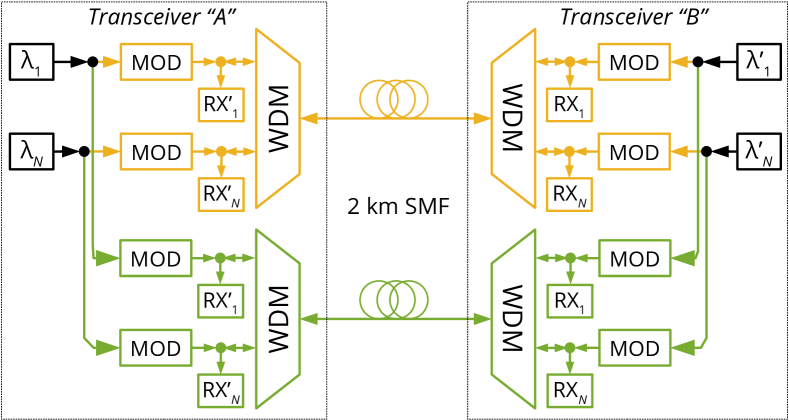
A high-level schematic of the proposed bi-directional architecture is shown in Fig. 3.1. Inside each transceiver, lasers are shared between the two directions, realizing a higher level of integration than two independent transceivers, reducing overall cost and power consumption. Then, each laser (operating in the O-band) is divided by -dB splitters and sent to two modulators, one for each fiber. A WDM coupler is used both to combine data from different channels and to separate the incoming WDM channels. Half of the incoming (using another 3-dB coupler) light is sent back to the modulator, which is suppressed by the isolators at the output of lasers.

This architecture achieves separation of data in two directions with -dB splitters, which reduces the power budget (compared to an MPO-based solution) by approximately -dB. This solution, which is simpler with respect to solutions previously discussed (circulator or different wavelengths), suffers from back-reflections. Assuming that a back-reflection occurs, data will interfere with the signal transmitted in the other direction, which has the same (nominal) frequency, so that it cannot be suppressed by WDM couplers.
To avoid this issue, we propose a slight frequency shift of the lasers inside one of the transceivers, called transceiver “B” in Fig. 3.1. This shift would be small enough to keep lasers at the same nominal wavelengths of the WDM grid. This operation is feasible, since – for Intra-DC applications – WDM grids allow wider tolerances than long-haul applications. For instance, the LAN-WDM grid has a frequency spacing of -GHz, and it is the most dense grid used in Intra-DC standards. The other grid widely used in Intra-DC is the CWDM grid, which has a wavelength spacing of nm, corresponding to THz in the O-band. Fig. 3.2 shows an example of this frequency shift. For the -th channel, the standard specifies a nominal central frequency and a range . This range is wider than the spectral occupancy of a channel to allow some tolerances. In this architecture, this tolerance is exploited by changing the central frequency of the transceivers to and . Those values are close enough to the nominal frequency such that both transceivers are compliant to the standard (which defines the selectivity of WDM filters). However, this approach requires a more precise wavelength control with respect to standard Intra-DC applications, since – as it will be shown later – this frequency shift must be greater than a minimum value.
3.3 Impact of reflection crosstalk
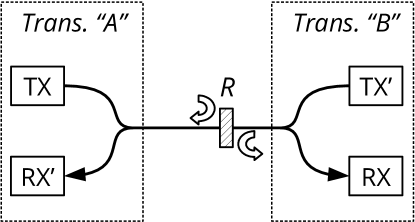
Let us assume the generic bi-directional architecture of Fig. 3.1, which is depicted (in a simplified form) in Fig. 3.3. In case of a back-reflection, a portion of the transmitted optical power is reflected back. The ratio between the incoming power and the reflected power is called reflectivity. In a bi-directional transmitter scheme, data generated by transceiver “A” gets reflected back to its receiver, which is tuned to receive data from transceiver “B” (indicated by ′ since it has a slightly different frequency). The same may happen in the other direction.
Usually, other than the reflectivity, another parameter is used, called Signal to Interference power Ratio (SIR), defined as the ratio between the optical power of the wanted signal and the optical power of the interfering (reflected) signal, measured immediately before the receiver. In this section, we will assume a simplified scenario where the line is lossless, i.e. fiber and connector losses are zero. In this case, assuming that , the SIR is simply the opposite of the reflectivity:
| (3.1) |
This issue has already been studied in details for NRZ signals, and takes the general name of coherent crosstalk, since the frequency of the interfering signal is very close to the frequency of the wanted signal. However, past studies [Gimlett:89] studied this effect in a different scenario, which is multi-path interference. In that context, multiple reflections () generate an interfering signal which is the sum of delayed copies of the signal itself, which have exactly the same frequency. Moreover, most of the models assume that the interfering signal is Gaussian-distributed. However, in [Attard:05], it was shown that for a few reflections, the “Gaussian” approximation is overly pessimistic. Since, in the considered architecture, the main source of interference is a single reflection, the model must not use the Gaussian approximation.
3.3.1 Theoretical model
To develop an analytical model, some simplifying assumptions have to be made. For this model, we adopted the same assumptions as [Attard:05, Sec. IV], which are here summarized:
-
1.
Signal and crosstalk are bit-aligned in time. This is a worst-case assumption, since PAM- transitions have lower power than the levels.
-
2.
Phase difference, due to laser phase noise, is constant within one symbol.
-
3.
Signaling use purely-rectangular PAM- pulses, without any bandwidth limitation at the transmitter and receiver.
-
4.
Receiver uses an ideal matched filter, i.e. a rectangular filter, without equalization.
-
5.
Signal and interferer are polarization-aligned. Other than being a worst-case approximation, in [Goldstein:95] it was shown that this situation happens more frequently than expected.
Using these assumptions, a fully analytical result can be obtained. Assuming that the transmitted PAM- symbol is interfering with the PAM- symbol transmitted in the opposite direction (and reflected), the two lasers are freqency-separated by and have a phase difference , and symbol duration is , the received signal before decision is:
| (3.2) |
Note that, in this equation, there is no time index, since this effect is not time-dependent. Also note that and refer to the symbols’ optical power. Full derivation of this formula is reported in Appendix LABEL:app:paminterf.
In this equation, interference is generated by two different sources:
-
•
The first source, , depends only on the SIR. This is called incoherent crosstalk, since it does not depend on the frequency separation. Unless is larger than the bandwidth of the WDM coupler, this term cannot be suppressed.
-
•
The second source depends on and . This term is (for small ) larger than the first one, which means that crosstalk can be effectively reduced by acting on .
Equation \eqrefeq:paminterf can be then used to compute the Bit Error Ratio (BER). Assuming that the received signal is impaired by additive white Gaussian noise with standard deviation (see Sec. 2.2.2 for details), the probability of a symbol error, given the transmitted and interfering symbols and , is
| (3.3) |
The expectation is performed over , which, assuming that is uniformly distributed between and , it has the following probability density function [Bertignono:16]
| (3.4) |
, instead, is/are the decision threshold/thresholds of symbol , which can be one or two, depending on the position of the symbol. Then, from \eqrefeq:pamser, calculation of the BER is straightforward.
3.3.2 Simulation tool
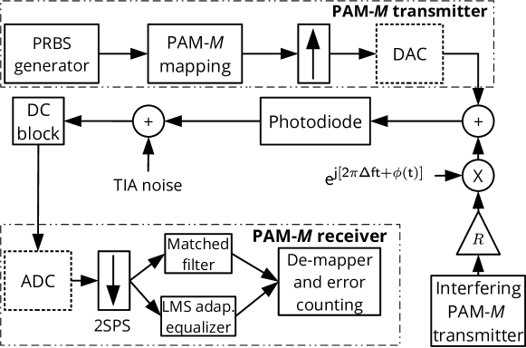
The theoretical model presented in Sec. 3.3.1 needs to be validated. To do so, we set up a PAM- time-domain simulation tool, whose schematic is shown in Fig. 3.4. A Pseudo Random Bit Sequence generator generates a bit sequence, that is mapped into a PAM- sequence with a finite extinction ratio. The signal is then upsampled with ideal rectangular pulses, and then low-pass filtered and quantized by a DAC. Then, another interfering PAM- signal is generated with random bits, multiplied by a complex exponential to apply a frequency and phase deviation, scaled by the reflectivity and added to the signal. As discussed in Sec. 3.3, link is assumed ideal, therefore is the inverse of SIR \eqrefeq:sirreflection. represents laser phase noise, and it is assumed to have a Lorentzian shape, with a -MHz linewidth.
At the receiver, the signal is low-pass filtered and quantized by an ADC and sampled at two samples per symbol. Then, it can be either filtered with an ideal matched filter, or by a fractionally-spaced Least-Mean Squares (LMS) adaptive equalizer. At the end, a slicer performs hard decision, followed by BER computation. Considering the KP4 code (see Sec. 2.2.1), we choose a conservative BER threshold of .
This simulator will be used both to validate the theoretical model and, in Sec. 3.4, to validate the experimental results.
3.3.3 Simulation results
| \topruleParameter | Value |
|---|---|
| \midruleSymbol rate | GBaud |
| Extinction ratio | dB |
| DAC/ADC | Ideal |
| Receiver | Matched filter |
| \bottomrule |
[b]0.48
 {subfigure}[b]0.48
The simulator was set up using the parameters summarized in Table 3.1. A GBaud PAM- signal is generated with an extinction ratio of dB and measured with a receiver with an equivalent noise current of and unit responsivity ( A/W). Since the model does not take into account bandwidth limitations, ADC and DAC are assumed ideal, and the receiver uses a simple matched filter. First, it is calculated the minimum ROP to transmit at the BER threshold without interference. Then, this “baseline” ROP is subtracted from the ROP of the other results with interference, obtaining the optical power penalty that is shown in Fig. 3.7. This operation has been adopted for all subsequent results of this chapter. Note that this result does not depend on the receiver noise current, thanks to the normalization to the no-interference ROP (“baseline”).
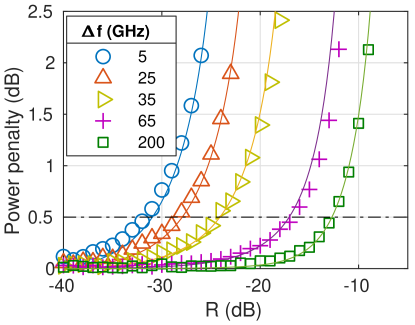
Results are shown in Fig. 3.7 as a function of the reflectivity and the laser spacing , where markers represents numerical simulations and solid lines were obtained with the analytical formula. It can be seen that the theoretical formula can accurately predict performance in a wide range of values of and .
Discussion
Fig. 3.7 shows the power penalty as a function of the reflectivity, for different values of . Regardless of the frequency spacing, power penalty keeps low for increasing reflectivity , up to a point where penalty suddenly increase. An increase of moves this “threshold” to stronger values of . By setting an arbitrary threshold at dB power penalty, some system-level consequences can be derived.
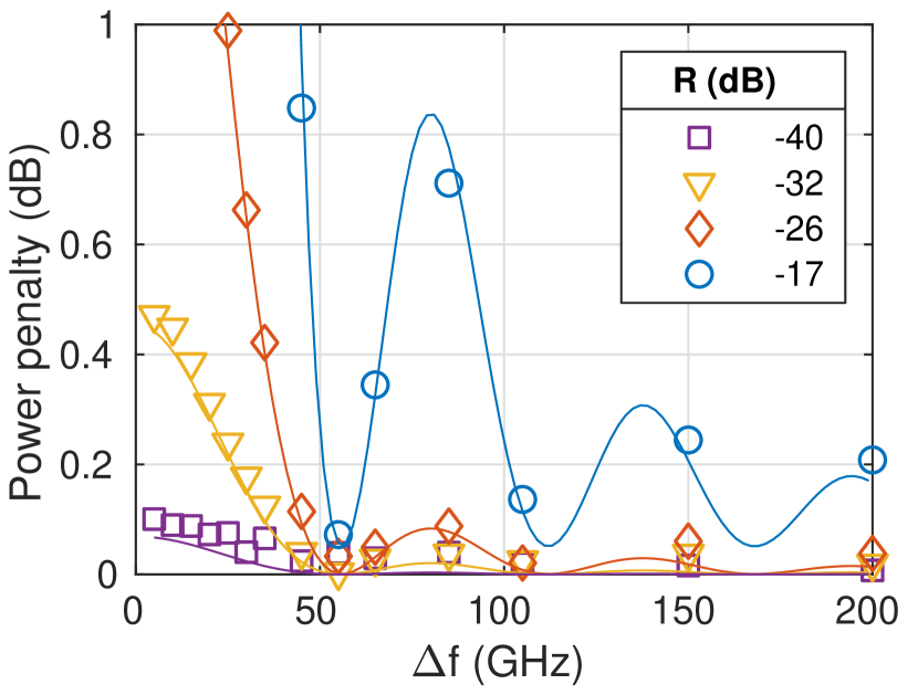
For small values of (e.g. GHz, blue circles in the figure), the threshold is approximately at dB. This value is too demanding; in fact, a single TIA-568 LC connector, widely used in data-centers, has a maximum specified reflectivity of dB. However, if is increased above the symbol rate (e.g. GHz, purple crosses in the figure), the threshold increases to dB, which is a reasonable value for real-world conditions. Fig. 3.7 shows the same results as Fig. 3.7, but as a function of the spacing. It is interesting to see that, for strong reflectivities, power penalty fluctuates, which is due to the function in \eqrefeq:paminterf.
To summarize, these results give two very important conclusions. First, the theoretical model is valid over a wide range of parameters. Second, and most importantly, the proposal of a slight change in to reduce back-reflection penalties, presented in Sec. 3.2, is feasible. A frequency shift in the order of the symbol rate is well within the ranges of the WDM grids adopted for Intra-DC applications.
Then, the last step to definitely prove the feasibility of the architecture is an experimental validation, which will be performed in next Sec. 3.4.
3.4 Experimental validation
3.4.1 Experimental setup

A high-level block scheme of the experiment is shown in Fig. 3.8. For simplicity, only one WDM channel was transmitted, since the purpose of the experiment is the evaluation of the back-reflection penalty at the same nominal wavelength. Moreover, due to the unavailability of O-band components, the experiment was performed in the C-band, which allowed the use of Erbium Doped Fiber Amplifiers (EDFAs) to recover the extra losses of the lumped components. Nevertheless, given the limited propagation distance, ASE noise inserted by the EDFAs was negligible with respect to receiver thermal noise. For propagation, we used a -km span of Dispersion-Shifted (DS) fiber, which has approximately the same dispersion curve in C-band as SMF in the O-band.
In the setup there are two transmitters. One is generating the channel under test with pattern PAM1 and the other one generates the interfering channel with a different pattern PAM2. Each of them is made of a Distributed Feedback (DFB) laser ( MHz linewidth), connected to a -GHz lithium-niobate optical modulator, which modulates the intensity of light based on a PAM- signal generated by a pattern generator. Before the interfering channel, a -dB coupler sends light from the channel under test (and reflections of the interfering channel) to a Variable Optical Attenuator (VOA), used to set the ROP, a photodiode and a real-time oscilloscope. Receiver Digital Signal Processing, performed offline, consists in a -tap (-spaced) adaptive equalizer, followed by hard decision and error counting.
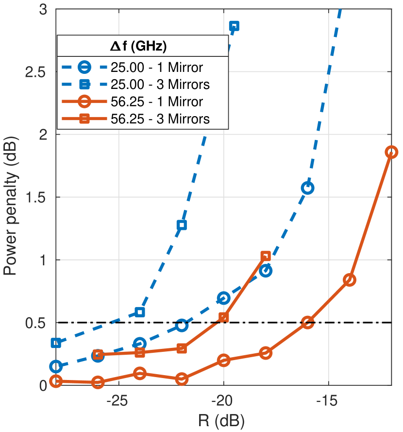
Back-reflections are inserted using three mirrors , and , connected to the fiber using -dB couplers and polarization controllers (PCs) to align polarization of the reflected light to the incoming signal. For the experiment, we either used one single reflector () or all of them, to emulate multiple reflections.
3.4.2 Results with single reflector
[b]0.48
 {subfigure}[b]0.48
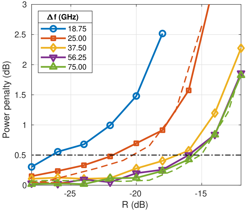
First, we run results with a single reflector ( of Fig. 3.8). This is the most important test, since, as previously discussed, single-reflections are the strongest sources of penalty. Results are shown in Fig. 3.11 for two PAM- symbol rates, GBaud and GBaud. The value of reflectivity has been normalized to the losses of the splitters and polarization controllers, so that, as done in previous section, the SIR is the opposite of \eqrefeq:sirreflection. Then, by tuning the receiver VOA, we calculated the minimum ROP for each combination of and at the FEC threshold, as done with the simulation. Afterwards, all results have been normalized to the minimum ROP without interference, to obtain the optical power penalty. Analyzing at the results of Fig. 3.11, the conclusions obtained in Sec. 3.3.3 are confirmed. At both symbol rates, a laser spacing greater than the symbol rate is sufficient to tolerate realistic back-reflections.
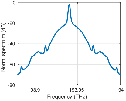
The transmitter had strong bandwidth limitations, even at 28 GBaud, as shown in the optical spectrum of Fig. 3.12. Therefore, the receiver had to use an adaptive equalizer. With this receiver, the hypothesis of the analytical derivation performed in Sec. 3.3.1 are not valid anymore, and its predictions cannot be compared with the experiment. Therefore, cross-validation with the experimental results was performed with the numerical simulator of Fig. 3.4, where we included transmitter bandwidth limitations and adaptive equalizer. Results of the simulations are shown as dashed lines in Fig. 3.11, where there is good agreement with the experimental results.
3.4.3 Three reflections
[b]0.48
 {subfigure}[b]0.48
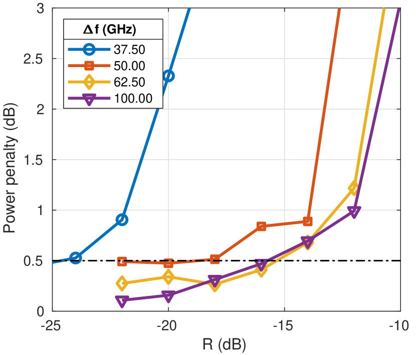
While the main source of penalty are single-reflections, multiple (three) reflections can be detrimental, since crosstalk becomes similar to a Gaussian disturbance [Attard:05]. To test this condition, we used the three mirrors , and of Fig. 3.8. The reflection of each mirror was tuned such that their reflected power is equal at the receiver. Results are shown in Fig. 3.15, as a function of the total reflectivity , for two different laser spacings, GHz (solid red lines) and GHz (dashed blue lines). Results are compared with single-reflections (circles) at the same value of , to show the additional penalty of multiple reflections.
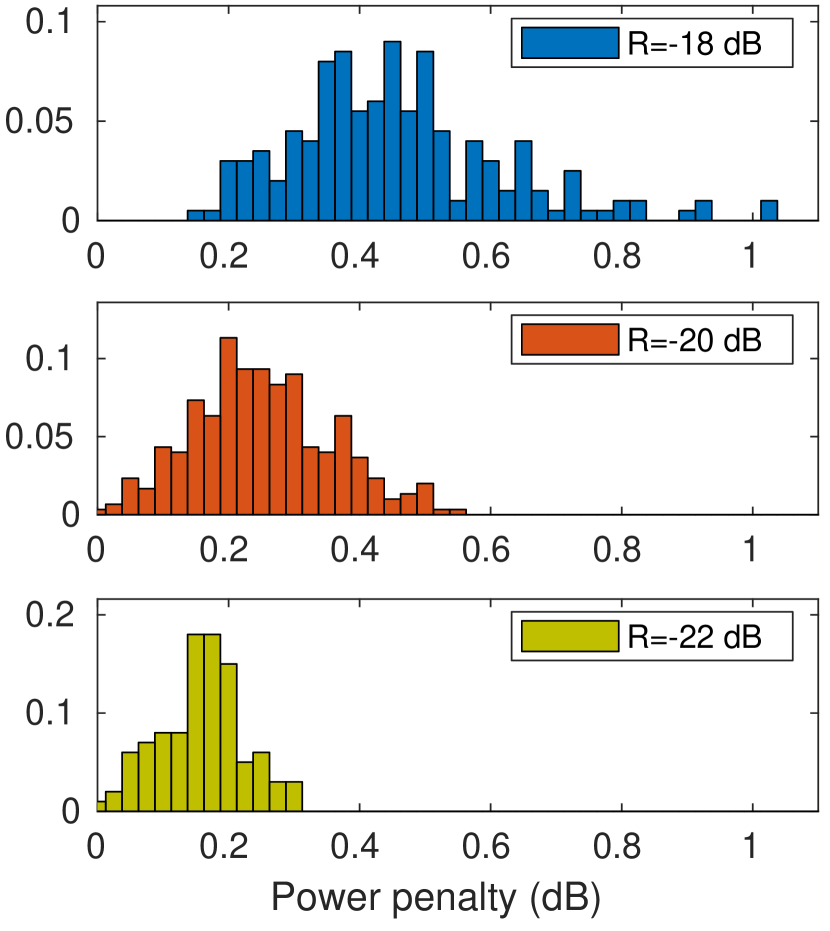
In the presence of multiple reflections, the power of the interfering signal is not deterministic anymore, since it is the sum of three contributions with a randomly changing phase (due to laser phase noise). Therefore, the penalty is not deterministic as well. Consequently, for each measurement, we captured waveforms on the oscilloscope, and Fig. 3.15 shows the worst result. The variation of penalty over different waveforms is shown in the histograms of Fig. 3.15 for three values of reflection (, and dB) and GHz.
At the dB power penalty line, three reflections have an additional dB penalty compared to a single reflection. This result is expected, since the sum of multiple reflections makes interference close to a Gaussian distribution, which is more detrimental than a single PAM interferer [Attard:05]. Consequently, these results with multiple reflections require an increase of the minimum to have acceptable back-reflection penalties. While, with a single reflection, it was sufficient a larger than symbol rate, in presence of multiple reflections should be larger than twice the symbol rate. Nevertheless, this value is still within the tolerances of Intra-DC WDM grids.
3.5 Conclusion and outlook
In this chapter, it was proposed a novel spatial-multiplexing architecture, which is able to double the per-laser capacity by using a standard duplex optical cable in both directions. The main issue of the proposed scheme are back-reflections, which generate crosstalk between channels transmitted in both directions. We found that, by applying a small laser frequency shift, in the order of twice the symbol rate, in one transceiver, the impact of back-reflections is reduced and becomes tolerable. However, it requires a tighter control of laser wavelengths.
The biggest limitation of this experimental evaluation is the absence of a real-time BER measurement, which is necessary to definitively prove the feasibility of the system, and will be performed in future research.
Capitolo 4 Single-Sideband Modulation for Inter-DC
This Chapter is focused on inter data-center connections, introduced in Sec. 2.3 of Chapter 2. First, the Discrete Multitone (DMT) modulation format will be presented as a potential alternative to PAM for IM/DD systems. Then, the single-sideband transmission (and reception) scheme will be presented as a hybrid solution between coherent and IM/DD for dispersion-uncompensated links. Then, a detailed comparison between IM/DD and SSB, using the DMT modulation format, will be performed over an -km link.
Content presented in this Chapter is based on [Randel:15, Pilori:masterthesis, Pilori_JLT:16, Pilori:ICTON2018].
4.1 Discrete multitone modulation
The goal of Intra-DC connections is transmission of high data-rates over distances in the order of km. This operation needs to be done at a cost that is substantially lower than long-haul coherent links. A common option to reduce cost is the use of limited-bandwidth components, at the expense of an additional OSNR penalty. Since, at those distances, OSNR values are high, this is a feasible solution. For this reason, modulation formats that are resilient to bandwidth limitations can be potentially beneficial to Intra-DC links. DMT is, in fact, a modulation format specifically designed to deal with limited-bandwidth channels. The goal of this section is briefly describing DMT, focusing only on its main characteristics and differences compared to other modulation formats.
4.1.1 Multi-channel transmission

DMT is a multi-channel modulation format. Fig. 4.1 shows a block diagram of a generic multi-channel communication system. At the transmitter, information bits are divided, using a serial-to-parallel converter, into transmitters. Then, the modulated signals are added and transmitted over the channel. At the receiver, receivers detect, respectively, the transmitted signals. At the end, a parallel-to-serial converter recovers the original stream of bits. These parallel channels are often called subcarriers.
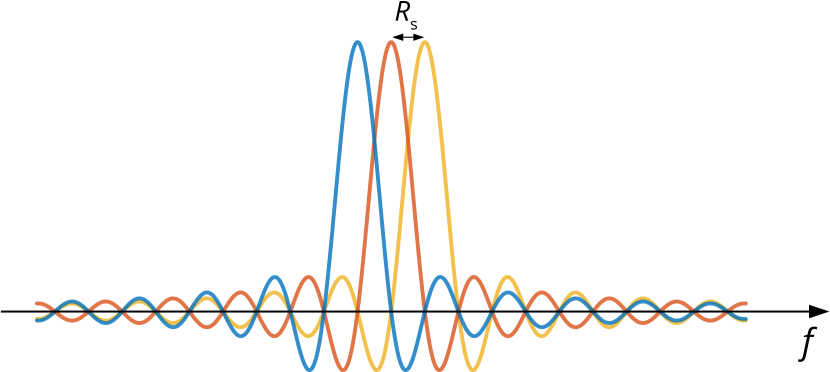
It is obvious that the parallel channels must be separated by a physical dimension to allow detection without interference. Usually, the channels are separated in frequency; there are two different methods to achieve frequency separation: Sub-Carrier Multiplexing (SCM), also called Frequency Division Multiplexing (FDM), and Orthogonal FDM (OFDM). In order to highlight the main differences between SCM and OFDM, Fig. 4.4 shows the spectra of SCM and OFDM, assuming transmission of three channels.
[b]0.65
{subfigure}[b]0.65
SCM
Sub-carrier multiplexing fully separates (in frequency) the channels, adding a small guard band between them. Channels are usually shaped with a steep (small roll-off) Root-Raised-Cosine (RRC) filter. SCM requires long (i.e. with many taps) filters at the transmitter and receiver, but it is more robust to various impairments, such as DAC/ADC bandwidth limitations [Bosco:2010]. Moreover, guard-bands reduce the overall spectral efficiency, making SCM feasible only with a limited number of subcarriers.
OFDM
With OFDM, as opposed to SCM, channels are spaced by exactly the symbol rate, without any guard band. This maximizes spectral efficiency, allowing the use of large numbers of subcarriers. The receiver is still able to separate, without interference, the channels because they are all orthogonal with respect to each other [Shieh:2008]. However, to preserve orthogonality, the receiver must be tightly synchronized with the transmitter. Moreover, in presence of memory in the channel (i.e. low-pass filtering), a cyclic prefix needs to be inserted at each OFDM symbol, reducing spectral efficiency.
Application to optical communications
Using coherent transmission and reception, OFDM and SCM can be directly applied to the optical channel, analogously to wireless transmission. In the past, these two formats were deeply studied and compared [Shieh:2008, Bosco:2010, Bosco:2011, Shieh:2011], and it was found that SCM is more suitable than OFDM to the coherent long-haul transmission scenario. In fact, (at least) one major vendor has successfully implemented SCM in their commercial transponder [Infinera:whitepaper].
For short-reach applications, single-channel transmission is still widespread. However, with the strong data-rate increase that will be required in the future [Winzer:2017], multi-channel modulation can be a potential solution. For this fact, this section will use DMT modulation as an example modulation format for Intra-DC applications.
4.1.2 DMT
In Sec. 4.1.1, OFDM and SCM were presented from a theoretical point of view, and applied to the coherent long-haul scenario. As discussed in Chapter 2, coherent detection is still too complex to be widely deployed for Intra-DC applications. Therefore, a direct-detection application of multi-channel transmission is preferable, and will be discussed in this section.
Hermitian symmetry
Discrete Multitone is a variant of OFDM that generates a real-valued (an OFDM signal is complex-valued) signal, which is suitable to be received with a direct-detection receiver. It was first developed at the beginning of the 1990s [Ruiz:1992] for copper-cable transmission, and subsequently adopted for the Digital Subscriber Line (DSL) standards.
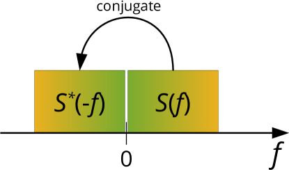
With DMT, assuming to have at the center of the spectrum, negative-frequency subcarriers are not modulated. Instead, the negative-frequency spectrum is a mirrored and conjugated copy of the positive-frequency spectrum. This operation is shown in Fig. 4.5, where the positive-frequency portion of an OFDM signal is mirrored and conjugated () to obtain the negative-portion of the spectrum. According to signal theory, this property is called “Hermitian symmetry”, which generates a real-valued time-domain signal. Obviously, this operation halves spectral efficiency, which is inevitable due to the loss of one dimension (the imaginary part).
Bit and power loading
DMT is usually employed in strongly frequency-selective channels, such as DSL. In this scenario, transmission quality (i.e. the SNR) is different among different subcarriers, strongly reducing performances if the same power and modulation format is applied to each subcarrier. Applying the “water-filling” power allocation [proakis2007digital], which assigns more power to higher-quality subcarriers, further enlarges the SNR difference between them.
This issue is solved by using bit loading, i.e. using different modulation formats on different subcarriers, based on their SNR. The most common bit-loading algorithm is the Levin-Campello algorithm [Campello:1999, Levin:2001]. A detailed overview of the algorithm, along with a pseudo-code representation, is available on [Pilori:masterthesis, Chapter 4].
4.1.3 Comparison with PAM
A comparison between DMT and PAM in a direct-detection scenario is out of the scope of this thesis. Nevertheless, in the past years, several comparisons have been published. Recent experiments [Zhong:2015, Eiselt:2018] found, on average, similar performances if non-linear equalization (e.g. decision-feedback equalization) is applied to PAM. At the end, the actual choice of modulation format will strongly depend on the scenario, optical components and maximum allowable DSP complexity.
4.2 Single side-band
As discussed in Sec. 2.3.2, SSB is a potential “hybrid” between coherent systems and IM/DD, that is suitable for dispersion-uncompensated links. In this Chapter, SSB will be compared to direct detection, using the DMT modulation format. However, it is important to remark that SSB is modulation-format agnostic, and it can be potentially applied to any format.
4.2.1 Basic principle
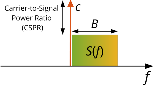
SSB is a technique that, in general, allows detection of the full optical field (magnitude and phase) with a direct detection receiver. The optical spectrum of an SSB signal is shown in Fig. 4.6. In the Figure, is a generic complex-valued coherent signal (e.g. OFDM, QAM, …), and is a carrier (e.g. laser light), with higher power than the signal. The ratio between the power of and signal power is called Carrier-to-Signal Power Ratio (CSPR). Application of SSB to real-valued signals, such as DMT, will be detailed in the next sections.
Assuming a complex-envelope representation around a central frequency set to the middle of the useful signal spectrum, the time-domain electric field of the signal in Fig. 4.6 can be written as:
| (4.1) |
where is the bandwidth of . After direct-detection with an ideal photodiode, the photocurrent becomes
| (4.2) |
This equation has three terms:
-
•
is a DC component, that can be easily suppressed at the receiver.
-
•
is the complex up-conversion of at frequency , allowing reconstruction of the complex-valued signal in the DSP. This comes at the expense of a larger receiver bandwidth.
-
•
is an interference term, called Signal-Signal Beating Interference (SSBI), and it must be suppressed at the receiver.
In conclusion, SSB allow detection of a single-polarization coherent signal with a direct-detection receiver. This operation increases spectral efficiency, becoming equal to a single-polarization homodyne coherent system. Moreover, it allows electronic dispersion compensation. The main drawbacks are two: increased receiver analog bandwidth (double with respect to an equivalent coherent system), and SSBI.
4.2.2 SSBI compensation
There are serveral methods to compensate (or avoid generation) of SSBI. The simplest method is based on the observation that is a low-pass signal. Then, by introducing an appropriate frequency gap between and , SSBI impact can be reduced [Peng:2009]. However, this solution requires an even-larger receiver bandwidth, making it unsustainable for high data-rate systems. Another possibility is the use of balanced photodiodes to optically remove SSBI [Ma:2013]. However, this operation requires a complete optical separation between signal and carrier. This needs steep optical filters and a frequency gap between signal and carrier. The most promising solution is digital SSBI compensation. In literature, several methods have been proposed [Peng:2009, Randel:15, Li:2016] with different complexity and effectiveness. Another option to avoid SSBI is the use of a Kramers-Kronig receiver [Mecozzi:2016], which is a DSP reception technique that, at the expense of higher DSP complexity, is able to fully suppress SSBI.
A comparison between SSBI compensation techniques is out of the scope of this thesis; the interested reader can refer e.g. to [Li:PhDthesis]. For this thesis, it was adopted the method presented in [Randel:15, Randel:patent], which offers good performances with a very low DSP complexity.
4.2.3 Generation of SSB signals
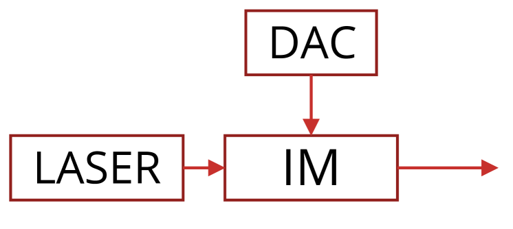
[b]0.45
 {subfigure}[b]0.45
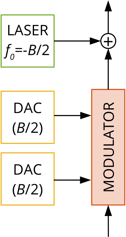
The transmitter is a critical part in the design of a SSB-based transmission system, since it requires the addition of a strong carrier at one edge of the signal spectrum. The two main methods to achieve this are summarized in Fig. 4.9. With the simplest method, shown in Fig. 4.9, a second laser, with a frequency difference between the transmit laser, adds the carrier after I/Q modulation. In this case, the signal is generated by two DACs with bandwidth , like a coherent transmitter. However, this solution requires two lasers, and a tight control of their frequency difference.
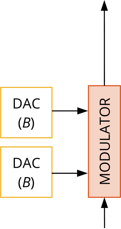
An alternative method is shown in Fig. 4.9. In this case, the two DACs require twice the bandwidth () to generate an SSB signal. Then, the carrier is added by intentionally leaking un-modulated light from the transmit laser. This is usually achieved by biasing the modulator to an appropriate point [Pilori:ICTON2018]. Other than bandwidth requirements, this solution increases modulator-induced non-linear distortions, but removes the requirement of a second laser.
In conclusion, the optimal transmitter structure for SSB strongly depends on the choice (and cost) of each component of the system. For the rest of this Chapter, it will be assumed an ideal transmitter.
4.2.4 SSB and DMT
In Sec. 4.2.1, SSB was presented from a general point of view. In particular, \eqrefeq:ssbgeneric defined a SSB electric field using a complex-valued signal . On the other end, Sec. 4.1.2 defined DMT as a real-valued signal. Apparently, this is a contradiction that makes DMT not compatible with SSB. With a slight abuse of notation, in an SSB-DMT system, only the electrical signal after the photodiode (neglecting DC and SSBI) is a DMT signal. In fact, the term SSB-DMT is not even universally adopted in the literature (e.g. [Schmidt:2008]).
For example, let us consider a general real-valued signal (e.g. DMT). The I/Q modulator generates the following SSB optical signal:
| (4.3) |
In this equation, denotes Hilbert transform, defined as the convolution with a linear filter whose frequency response is
| (4.4) |
The addition, on the imaginary axis, of the Hilbert transform of eliminates the negative frequencies of . Since the negative spectrum of any real-valued signal is a copy of the positive spectrum, this operation does not lose any information. The spectrum of the signal is identical to the spectrum of an SSB signal \eqrefeq:ssbgeneric, except from a frequency shift. Detecting this signal with an ideal photodiode generates a photocurrent:
| (4.5) |
This equation is equivalent to \eqrefeq:ssbgenericpd, since it contains the original signal , the DC component and SSBI.
This notation allows the application of SSB to any real-valued modulation format (such as DMT or PAM). It is different than the “traditional” SSB notation introduced in Sec. 4.2.1, but equivalent to it. Since the purpose of this Chapter is the comparison with IM/DD systems, which use real-valued signals, this is the notation that will be adopted.
4.3 Back-to-back comparison
After introducing DMT and SSB, this Section will be devoted to a detailed comparison between intensity modulation and SSB in a back-to-back scenario. In this section, another transmission technique, called Vestigial Side-Band (VSB), will be introduced, as a hybrid between IM and SSB. To highlight the differences between IM and VSB/SSB, Intensity Modulation will be called Dual Side-Band (DSB). The comparison will be first performed using analytical evaluations, which will be then validated using time-domain DMT numerical simulations.
4.3.1 Methodology
Comparison of different transmission techniques (IM, VSB and SSB) is, in general, not a trivial operation. Therefore, some assumptions have to be made in order to perform a fair comparison.
Modulation
Simulations will adopt the DMT modulation format. In general, evaluation of system performances with DMT requires transmission of two signals. First, a test DMT signal, using a fixed modulation format (e.g. 16-QAM) on all subcarriers, is transmitted. The receiver uses this test signal to calculate the per-subcarrier SNR, which is then fed to the bit and power loading algorithms. These algorithms generate a table which, for each subcarrier, gives the optimal modulation format and relative transmit power. This table is then given to the transmitter, which generates the “real” transmit signal. Then, the receiver measures the BER, comparing it with the FEC threshold.
It is obvious that this operation is quite onerous in terms of complexity. Therefore, for this comparison, we adopted a simplified approach, based on the “equivalent SNR” principle. According to theory [Cioffi:book], an ideal multi-channel modulation achieves the same performance as a single-channel transmission with an equivalent SNR which is the geometric mean of the per-subcarrier SNR:
| (4.6) |
This value is easy to evaluate if the SNRs are expressed in decibels; in this case, the equivalent SNR is simply the arithmetic mean of the per-subcarrier SNRs.
| \topruleParameter | Value |
|---|---|
| \midruleModulation | -QAM |
| DAC sampling rate | Gs/s |
| FFT size | |
| Modulated subcarriers | |
| BER threshold | |
| SNR threshold | dB |
| \bottomrule |
Therefore, in this comparison we transmitted only a test signal, whose parameters are summarized in Table 4.1. The receiver evaluates the equivalent SNR by direct comparison with the transmitted signal, which is then used as performance indicator.
Simulation setup
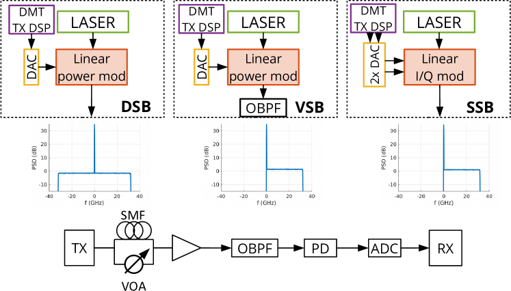
The general schematic of the simulations performed in this Chapter is shown in Fig. 4.10. On the top, there are the three transmitter structures of the three transmission methods: DSB, VSB and SSB. DSB (synonym for intensity modulation), is the simplest structure, since it requires one DAC and a linear power modulator, which linearly converts the voltage from the DAC to an optical power. VSB, with respect to DSB, adds an optical band-pass filter (OBPF) to suppress one side-band, emulating a SSB signal. On the other end, SSB requires (at least) two DACs (same as Fig. 4.9) and a linear I/Q modulator, which converts DAC voltages to an electric field. Examples of optical spectra after the transmitters are shown in the middle of Fig. 4.10.
Transmission line (bottom of Fig. 4.10) is very simple. After the transmitter, signal is transmitted over a certain length of optical fiber, amplified with an EDFA, band-pass filtered with an ideal OBPF and detected with a photodiode. For the back-to-back comparisons, fiber is replaced by a VOA. The presence of an EDFA adds ASE noise, which will be taken into account in the OSNR. Since, for a DMT signal, it is not trivial to define a symbol rate, the OSNR will be evaluated on a nm bandwidth, corresponding to GHz in the C-band.
4.3.2 SSB performance
Let us consider transmission of an SSB signal , defined in \eqrefeq:ssbtx. The most important parameter in an SSB transmission is the CSPR, as shown in Fig. 4.6. Since the Hilbert transform is an all-pass filter, power of the real and imaginary parts are the same and equal to , where is the variance of . Therefore, the CSPR of an SSB system can be expressed as
| (4.7) |
Direct detection
This signal is transmitted in the back-to-back setup shown in Fig. 4.10. ASE noise is added by the EDFA on both polatizations. Then, the signal is ideally band-pass filtered to remove out-of-band noise and detected by the photodiode. Assuming, for simplicity, unit responsivity, the photocurrent is
| (4.8) |
Due to the OBPF, noise-noise beating can be neglected. Removing this contribution, and the DC tone , the photocurrent can be expressed as
| (4.9) |
This equation contains the usual two terms: and SSBI. The main difference with respect to \eqrefeq:ssbcurrentnonoise is the presence of ASE noise, which allows evaluation of the equivalent SNR from the OSNR. Assuming that the SSBI compensation algorithm is able to completely remove SSBI, the SNR can be expressed as
| (4.10) |
DMT simulations
As previously discussed, the analytical result in \eqrefeq:ssbosnr will be validated using the DMT modulation, whose parameters were summarized in Table 4.1. We remark again that the choice of DMT modulation is just an example, since SSB can be potentially combined with any modulation format.
Results are shown in Fig. 4.11, where the equivalent SNR is shown as a function of the CSPR for a fixed OSNR, equal to dB measured over a -nm bandwidth. Fig. 4.11 contains the analytical result \eqrefeq:ssbosnr (dotted line) and DMT simulations, without (dashed-dotted line) and with SSBI compensation [Randel:15] (solid line).
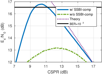
At low values of CSPR, main noise source is SSBI. This is explained the -factor that multiplies in \eqrefeq:ssbphotocurrent. Since \eqrefeq:ssbosnr does not take into account SSBI, the formula is not accurate at low CSPRs. For high values of CSPR, instead, performance is dominated by ASE noise, and \eqrefeq:ssbosnr becomes an accurate upper-bound of performances. Therefore, there exist an optimal CSPR, which represents a balance between SSBI and ASE noise. Moreover, Fig. 4.11 clearly shows the effectiveness of SSBI compensation. Even if the implemented algorithm [Randel:15] is one of the simplest, it brings a dB SNR gain at the optimal CSPR. This significant advantage makes SSBI compensation a strict requirement for SSB systems.
4.3.3 DSB performance
An intensity-modulated, also called DSB, signal can be expressed as
| (4.11) |
In this equation, is the average optical power and is a clipping function between and , defined as:
| (4.12) |
A first comparison between DSB and SSB can be done by comparing the transmitted signals \eqrefeq:dsbtxsignal and \eqrefeq:ssbtx. DSB requires a square-root operation, which needs clipping to avoid zero-crossings. This means that, while generation of an SSB signal is performed using only linear operations (Hilbert transfrom), transmission of a DSB signal requires two non-linear operations (clipping and square root). These operations, as it will be shown later, require several approximations in order to derive analytical results.
The parameter is used to tune the amount of clipping. It is customary to define a clipping ratio
| (4.13) |
which means that the signal is clipped between . The clipping ratio is an important design parameter of a DSB-DMT system [Nadal:2014], since a DMT signal has a higher Peak-to-Average Power Ratio (PAPR) compared to single-channel modulation formats.
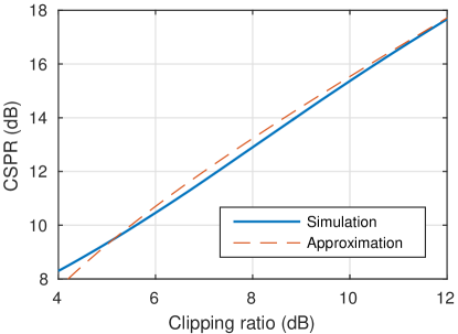
Clipping ratio and CSPR
The definition of clipping ratio is surprisingly similar to the CSPR for SSB \eqrefeq:ssbcspr. In fact, they both refer to a ratio between carrier and modulated power. Therefore, in order to perform a fair comparison between SSB and DSB, it is important to find a relation between these two parameters. For this derivation, we will assume that is a DMT signal, which means that is assumed to be Gaussian-distributed.
For a generic signal , the CSPR can be defined as the ratio between the un-modulated and modulated optical power; in formula,
| (4.14) |
where defines expectation and variance. Substituting the definition of DSB signal \eqrefeq:dsbtxsignal into \eqrefeq:csprdefinition allows obtaining an expression of the CSPR for a DSB signal. However, \eqrefeq:dsbtxsignal contains two non-linear operations, square root and clipping. Therefore, some approximations needs to be performed.
First, the square root can be expanded with a Taylor’s series expansion, assuming :
| (4.15) |
where
| (4.16) |
If , then clipping effects can be neglected, and can be assumed a Gaussian random variable (like ) with zero mean and variance . Substituting \eqrefeq:dsbtaylor into \eqrefeq:csprdefinition allows obtaining:
| (4.17) |
After simple mathematical operations, the final result is
| (4.18) |
Then, neglecting clipping, the variance of is
| (4.19) |
This expression allows a fully-analytical relation between clipping ratio and CSPR. Fig. 4.12 shows an example, where the analytical expression is compared with a numerical simulation, assuming DMT modulation. For high values of CSPR, the analytical expression is very accurate, making it suitable for comparing DSB and SSB modulations at the same values of CSPR.
Direct detection
With the same assumptions made in Sec. 4.3.2, the phtocurrent of a DSB signal can be expressed as
| (4.20) |
From this expression, neglecting the effects of clipping, the equivalent SNR can be expressed as:
| (4.21) |
Using the relations derived before, it is possible to convert the clipping ratio to the CSPR, allowing a direct comparison between SSB and DSB. A back-to-back result with DSB-DMT modulation will be shown in the next section, where it will be compared with SSB and VSB modulation.
4.3.4 VSB performance
VSB is a “hybrid” transmission scheme between DSB and SSB. It uses the simple DSB transmitter structure, but it adds a steep optical filter that suppresses negative frequencies. While, at a first sight, the signal may seem identical to SSB, it is not. The main difference is the presence of the two non-linear operations (square root and clipping), not present in SSB. As it will be shown later, these operations decrease the effectiveness of VSB transmission.
Assuming an ideal filter, a VSB signal is expressed as a function of the DSB transmit signal \eqrefeq:dsbtxsignal:
| (4.22) |
Direct detection
Applying the same approximations as previous sections, the photocurrent can be expressed as
| (4.23) |
Let us compare this equation with DSB photocurrent \eqrefeq:dsbphotocurrent. The first two terms, apart from scaling factors, are identical. However, there is a third quadratic term, which represents interference, and it is similar to SSBI in SSB systems. For simplicity, this term will be called SSBI as well.
A very simple compensation algorithm can be designed, similarly to [Randel:15]. The VSB “SSBI” can be estimated with
| (4.24) |
where is a free optimization parameter.
DMT simulations
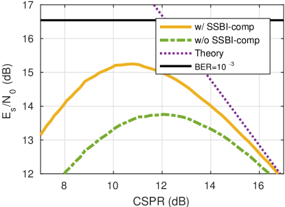
Fig. 4.13 shows the equivalent SNR of a VSB-DMT system, in back-to-back at a fixed dB. The CSPR have been calculated from the clipping ratio using the relations obtained for DSB. These results are similar to SSB (Fig. 4.11): at low CSPR, system is mainly impaired by SSBI. At high CSPR, system is impaired by ASE noise. SSBI compensation is somehow less effective than SSBI, but gives still a significant performance improvement.
4.3.5 Final comparison
[b]0.49
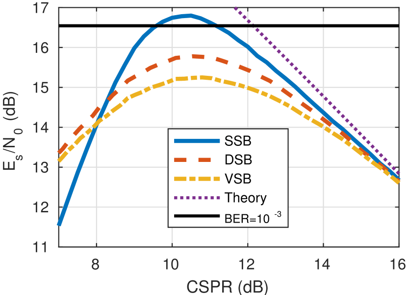 {subfigure}[b]0.49
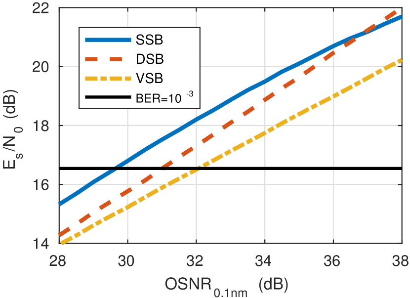
With the relation between CSPR and clipping ratio, DSB, VSB and SSB can be directly compared at fixed OSNR, fixed modulation format and CSPR. Results are shown in Fig. 4.16. For asymptotically high values of CSPR, where performance is limited by ASE noise, the three variants obtain approximately the same SNR. This allows to conclude that, even if spectral occupation is different, the three variants have the same performance with ASE noise. Performance differ, instead, at medium/low CSPRs. At very low CSPR, SSBI with SSB modulation is very strong, making DSB/VSB more effective. However, at the optimal CSPR, SSB is more effective. This is explained both by the effectiveness of the SSBI mitigation technique, but also by the absence of non-linear operations in signal generation.
Fig. 4.16 shows instead the performance, at the optimal CSPR, for different values of OSNR. Close to the FEC threshold, SSB performs better. For increasing values of OSNR, SSB loses some performance with respect to DSB. In both results, VSB has the worst performance, which is explained by the combination of non-linear operations and SSBI.
Final remarks
From the results presented in this sections, some conclusions can be already made:
-
•
There is a direct relation between CSPR and clipping ratio, allowing a direct comparison between intensity-modulation (DSB-VSB) and field modulation (SSB).
-
•
Performance with respect to ASE noise is identical to all the three methods.
-
•
At the optimal CSPR, in the considered scenario, SSB is the optimal transmission technique.
-
•
VSB suffers from both transmitter non-linearities and SSBI, making it the lowest-performing modulation format in back-to-back.
4.4 Impact of chromatic dispersion
After comparing the three formats in back-to-back, the goal of this section is the comparison over km dispersion-uncompensated SMF, which is a typical distance for Inter-DC links. Given the limited reach, Kerr effect and PMD can be easily neglected, and the only impairment is chromatic dispersion. Therefore, this section will just focus on its impact on the three modulation formats.
It is well-known that a SSB/VSB signal is resistant to chromatic dispersion [Yonenaga:1993]. On the other end, DSB signals are severely impaired by chromatic dispersion. The goal of this section is to show the effect of CD on DSB signals, and provide a full comparison between the three techniques with different amounts of CD.
4.4.1 Effect on DSB
Chromatic dispersion is modeled as an all-pass filter , whose Fourier transform is
| (4.25) |
In this equation, is the distance, is the frequency in complex baseband, while is the chromatic dispersion parameter. For SMF, usually .
With this definition, the received electric field of a DSB signal, before the photodiode, can be expressed as (in one polarization):
| (4.26) |
where denotes convolution. Since is an all-pass filter, it does not affect noise. To obtain an analytical formulation, the square-root in the DSB signal \eqrefeq:dsbtxsignal needs to be expanded with a Taylor’s series expansion, up to the second order. The result is
| (4.27) |
where is defined in \eqrefeq:dsbclipdef. After ideal photodetection, neglecting noise-noise beating and DC components, the photocurrent is