Dark vertical conductance of cavity-embedded semiconductor heterostructures
Abstract
We present a linear-response nonlocal theory of the electronic conductance along the vertical (growth) direction of a semiconductor heterostructure embedded in a single-mode electromagnetic resonator in the absence of illumination. Our method readily applies to the general class of n-doped semiconductors with parabolic dispersion. The conductance depends on the ground-state properties and virtual collective polaritonic excitations that have been determined via a bosonic treatment in the dipole gauge. We show that, depending on the system parameters, the cavity vacuum effects can enhance or reduce significantly the dark vertical conductance with respect to the bare heterostructure.
I Introduction
Semiconductor heterostructures such as quantum wells (QW) and superlattices are the building blocks of important optoelectronic devices working in the mid and far infrared, such as photodetectors Gendron et al. (2004); Jagadish et al. (2011) and quantum cascade lasers Faist et al. (1994); Köhler et al. (2002). In the case of infrared photodetectors, the photo-induced vertical electrical current along the growth direction of the heterostructure is the key detected quantity. The sensitivity of a photodetector is limited by the so-called dark current, i.e. the current without illumination Jagadish et al. (2011). Several experimental and theoretical studies have investigated such systems Levine et al. (1990); Zussman et al. (1991); Liu et al. (1993), pointing out that the main origin of the dark current at low temperatures is the electron tunneling through potential barriers Levine (1993). Recently, an improvement of the performances of Quantum-Well Infrared Photodetectors (QWIP) has been demonstrated for arrays of heterostructures embedded in photonic resonators Palaferri et al. (2018).
Recent transport experiments in cavity-embedded organic semiconductors Orgiu et al. (2015); Nagarajan et al. (2018) and in-plane magnetotransport measurements in cavity-embedded high-mobility two-dimensional electron systems Paravicini-Bagliani et al. (2019) have shown that the linear-regime electronic conductance of a material can be significantly affected by a cavity electromagnetic resonator even in the absence of illumination. Early theoretical works exploring the role of a cavity on transport have focused on cavity-modified excitonic linear transport Schachenmayer et al. (2015); Feist and Garcia-Vidal (2015) and charge nonlinear conduction Hagenmüller et al. (2017) for chains of two-level systems in the nonlinear regime where electrons are injected in the excited levels. A recent theoretical work Bartolo and Ciuti (2018) on in-plane magnetotransport in the presence of Landau electronic levels has shown how virtual polariton excitations can control the charge transport in the linear regime. Indeed, light-matter interaction can play a pivotal role in determining the electronic transport properties without illumination especially if the strong Dini et al. (2003a) or ultra-strong coupling regime Ciuti et al. (2005); Anappara et al. (2009); Günter et al. (2009); Todorov et al. (2010) is achieved.
In this paper, we report a theoretical study of the electronic linear-regime conductance of a cavity-embedded generic n-doped semiconductor heterostructure with parabolic dispersion, such as n-doped GaAs. Our theory considers the electromagnetic-vacuum effects on the conductance: no real photons are injected or created in the resonator. Based on a bosonized Hamiltonian, we calculate the vertical conductance in the growth direction within a nonlocal linear-response Kubo approach Bruus and Flensberg (2004). In order to describe the collective electronic effects, we consider the system Hamiltonian in the dipole gauge Babiker and Loudon (1983); Todorov and Sirtori (2012); De Bernardis et al. (2018); Cortese et al. (2019) where two interaction terms emerge, describing respectively the so-called depolarization shift and the light-matter coupling. The present general framework is applied to quantum well heterostructures. Numerical results showing how the dark conductance is controlled by the cavity without illumination are presented.
The article is organized as follows. In Sec. II, we introduce the general theoretical bosonic framework to determine collective light-matter excitations. In Sec. III, within a many-body nonlocal Kubo formalism we provide the general expression for the dark vertical conductance for n-doped heterostructures depending on the properties of the ground state and of the polariton excitations. Numerical results for specific heterostructures are presented and discussed in Sec. IV. Finally, we draw our conclusions and perspectives in Sec. V. The most technical details about the theoretical model are reported in Appendix A and B.
II Hamiltonian framework and collective light-matter states
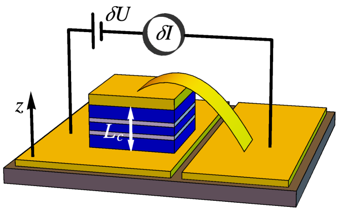
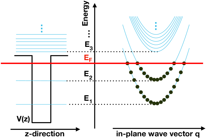
The system considered here is an arbitrary n-doped semiconductor heterostructure with small non-parabolicity epitaxially grown along the direction and embedded in a single-mode electromagnetic cavity. Single-mode electromagnetic resonators with tunable frequency can be obtained, for example, via LC-like structures Lee et al. (2010); Todorov and Sirtori (2014); Paulillo et al. (2014, 2017) (see Fig. 1). We assume the electrons to be free in the transverse direction where is the transverse area. The single-particle electronic eigenfunctions can be written as
| (1) |
where is the in-plane electron position and the in-plane wavevector. The eigenfunctions and their energies , are found by solving the one-dimensional Schrödinger equation for the motion along . Within the effective mass approximation Klingshirn (2007), the latter reads 111For simplicity, we neglect here the variation of effective mass along the heterostructure.:
| (2) |
with the effective mass and the potential describing an heterostructure of arbitrary shape. The in-plane energy dispersion of the state is , as sketched in Fig. 2. In the second quantization framework, it is convenient to introduce the fermionic operators () which annihilate (create) an electron in the -th band with wave-vector . In the absence of interactions, the many-body ground state is a Fermi sea with only the first subbands populated (cf. Fig. 2), namely:
| (3) |
where , is the Fermi wave vector associated with the -th band, while is the electronic and photonic vacuum. To describe the light-matter interaction for the heterostructure it is convenient to introduce collective electronic excitations Ciuti et al. (2005); Todorov and Sirtori (2012); Cortese et al. (2019) described by the operators
| (4) |
for and . The number is the difference between the occupation numbers in the two conduction subbands and ensures the normalization of the state . To simplify the notation, we compact the double index into , assuming that any sum on such index runs over all the index pairs satisfying and , unless differently specified. Note that in the limit where the operators satisfy bosonic commutation relations, that is De Liberato and Ciuti (2009) 222More specifically, with the population operator in subband and . As long as one considers states with a total number of excitations much smaller than , one has De Liberato and Ciuti (2009) . This implies that within a few-excitation subspace one can consider ..
The total Hamiltonian of the considered system can be arranged as the sum of four terms:
| (5) |
where we will neglect all constant contributions.
The noninteracting electronic contribution can be written in terms of the operators introduced in Eq. (4) and of the transition energies 333This can be done by projecting the full electronic Hamiltonian over the manybody excited states Todorov and Sirtori (2012); De Liberato (2009):
| (6) |
In the following, we wish to consider the Hamiltonian for an arbitrary semiconductor heterostructure embedded in a single-mode photonic cavity. Calling the frequency of the photon mode, the bare cavity contribution to the system Hamiltonian is given by
| (7) |
where () is the bosonic annihilation (creation) operator for a cavity photon.
To describe electromagnetic interactions, we will work here in the dipolar gauge Babiker and Loudon (1983); Todorov and Sirtori (2012), giving rise to two interaction terms. The first describe the coupling between the cavity photon mode and the collective intersubband excitations:
| (8) |
where the collective vacuum Rabi frequency reads Todorov and Sirtori (2012)
| (9) |
with the cavity length, the dielectric constant of the material filling the cavity, and
| (10) |
A relevant quantity indicating the strength of the light-matter coupling of a given transition is the resonant Rabi coupling . Note that the light-matter interaction Hamiltonian (8) includes both resonant and anti-resonant (counter-rotating wave) terms. The second interaction term is called depolarization shift Hamiltonian, which describes the self-interaction of the electronic polarization. In the considered system, it reads Todorov and Sirtori (2012)
| (11) |
where
| (12) |
The depolarization Hamiltonian is due to the collective part of the Coulomb interaction Lee and Galbraith (1999); De Liberato and Ciuti (2012). The other Coulomb terms are responsible for non-collective electron-electron scattering which will be neglected here.
In this work, we will focus on the case where all the subbands are macroscopically occupied. In this limit, the collective excitations behave as bosons and the Hamiltonian (5) is quadratic in the bosonic operators and . Hence, the eigenstates of the system can be determined by performing a Hopfield-Bogoliubov transformation Hopfield (1958); Ciuti et al. (2005); Nataf and Ciuti (2010); De Liberato and Ciuti (2012). The Hamiltonian can be diagonalized by introducing the bosonic hybrid light-matter polaritonic annihilation operators
| (13) |
To ensure the bosonic commutation relations , the coefficients must satisfy the hyperbolic normalization
| (14) |
In terms of such polariton operators, the total Hamiltonian (5) reads
| (15) |
The Hopfield-Bogoliubov coefficients and the polariton frequencies are determined by solving the eigenvalue equation , where the vector and the matrix is given explicitly in Appendix A, Eq. (37).
III Dark vertical Conductance
Our goal in this section is to derive an expression for the dark vertical conductance of the cavity-embedded heterostructure, i.e. the linear-regime electronic transport along the growth direction without illumination. In order to do so, we first determine the nonlocal conductivity via a linear-response Kubo approach Bruus and Flensberg (2004); Girvin and Yang (2019). Specifically, we are interested in the linear response when a small bias voltage is applied along the vertical (growth) direction between the two leads at the edges of the sample separated by the cavity spacer length [cf. Fig. 1].
Assuming that the heterostructure is translationally invariant in the -plane, but not along the growth direction , the electric field within the sample depends on but not on . This allows us to simplify the general Kubo expression by integrating out the transverse directions, as detailed in Appendix B. The field in the direction and the voltage are related by with
| (16) |
The variation of current density in the low-temperature limit is determined through the non-local response function via
| (17) |
with
| (18) |
where are the many-body ground () and excited () states of the system considered, being the corresponding energies. The quantity depends on the phenomenological scattering time Bruus and Flensberg (2004); Allen (2006). For purely electronic excitations, corresponds to the Drude transport scattering time . Finally, the operator is obtained from the -component of the paramagnetic current density operator, upon integration on the transverse plane:
| (19) |
Note that the inhomogeneity of the semiconductor heterostructure implies that the induced current actually depends on [cf. Eq. (17)]. As a result, applying an infinitesimal bias between the leads at , implies a -dependent change of the electronic charge density where . In other words, while the total charge is conserved in the semiconductor heterostructure, there are local variations of the charge density. This explains why is not constant along the semiconductor heterostructure. As an example, it can be analytically proven from the general linear response Kubo expression applied to and for the case of a noninteracting system, that the following continuity expression holds
| (20) |
where is the inelastic scattering time (the same for all subbands). Indeed, this expression shows the link between the induced current and the dissipation through charge accumulations. In the case of an interacting system, an analogous continuity equation holds with a more complex form.
The derivation of the conductance from the two-point response function in non-translationally-invariant systems is a subtle task which has been addressed in detail for elastic scattering in disordered systems Baranger and Stone (1989); Kane et al. (1988). The application of a bias across the sample induces a current coming out of the lead at (Fig. 1). The latter is related to the current density (17) by .
Assuming a homogeneous flow in the metallic contacts, such a must be also equal to the current entering through the lead at , that is, . To ensure this, we impose periodic boundary conditions to the functions when solving the Schrödinger equation (2). With this choice, definitions (10), (18), and (19) imply , which in turns ensure the periodicity of the current at the leads.
Qualitatively, we can assume the variation of the electric field to be negligible, so that the current reads:
| (21) |
from which the general expression for the two-probe conductance is
| (22) |
III.1 Conductance for non-interacting electrons
Let us first consider the behavior of a non-interacting system (no light-matter interaction, no depolarization shift, i.e. ). In this case and the only excited states connected to the ground state via are , which are states containing a collective electron-hole excitation above the Fermi sea. This simplifies Eq. (18) to the form
| (23) |
where . The noninteracting conductance reads
| (24) |
III.2 The cavity case:
conductance in the absence of illumination
In presence of interaction with the cavity quantum field, the manybody ground state of the system differs from the noninteracting Fermi sea, that is, . The cavity-dressed polaritonic excited states are defined by . The current operator (19) can be suitably rewritten exploiting the inverse of Eq. (13): . Thus, equation (18) can be easily applied to the new set of dressed manybody states to get
| (25) |
with
| (26) |
This finally gives the dark vertical conductance
| (27) |
Note that several effects contribute in determining how the cavity dark conductance (27) differs from the non-interacting one (24). First, the electronic states are dressed by photonic ones due to the interactions, which can strongly modify the spatial localization of the manybody wavefunctions. This determines the spatial shape of and is responsible for what we call the orbital renormalization of the conductance. Second, the interactions change the energetic cost associated with a polaritonic transition, thus altering the conductance. The third effect is the modification of the scattering times , which are associated with excited states having a mixed light-matter nature Bartolo and Ciuti (2018). These hybrid scattering times are a weighted combination of the Drude electronic scattering time and of a photonic transport scattering time :
| (28) |
where the electronic weight of the polariton created by is
| (29) |
Note that is not the photon lifetime inside the resonator, but a transport scattering time expected to be much longer Bartolo and Ciuti (2018). In what follows, we will consider , implying .
III.3 Two-subband approximation
In general, there is a subtle interplay between orbital, energetic and scattering-time effects determining the conductance of a cavity-embedded heterostructure. One can get some analytical insight in the special case in which one transition gives a dominant contribution to the conductance. This is the case, for instance, when one transition frequency is significantly smaller than the others, since high-frequency terms are quickly suppressed in the sums of Eqs. (24) and (27). In this context, the four-by-four Hopfield-Bogoliubov matrix (38) can be analytically diagonalized.
Let be the two-component index associated with the dominant transition, the noninteracting conductance reads
| (30) |
Making use of the exact relation holding for Hopfield coefficients Bartolo and Ciuti (2018)
| (31) |
the cavity dark conductance can be recast as
| (32) |
Note that in this one-transition approximation there are only two polaritonic branches: the lower () and upper () one.
Two relevant limits can be addressed. First, let us consider the limit , where only the depolarization shift effect matters. In this case, we get
| (33) |
The second limit is that of a high-frequency resonator: . The asymptotic value of the conductance reads
| (34) |
Note that one always has due to the Cauchy-Schwartz inequality
| (35) |
In the considered limits, since there is no scattering-time hybridization effect, the conductance modification is solely due to orbital and energetic effects. We see that the interactions always reduce the conductance with respect to the noninteracting case in the considered limits. It is also interesting to note that
| (36) |
IV Numerical results for quantum well structures
In order to understand the impact of the cavity on the physical properties of the embedded heterostructure, we consider some paradigmatic examples. We study both the case of a single quantum well and of a multiple quantum well heterostructure. For all the numerical results presented in this paper, we carefully verified that convergence was reached by increasing the number of intersubband transitions up to a large enough value.
IV.1 Single Quantum Well
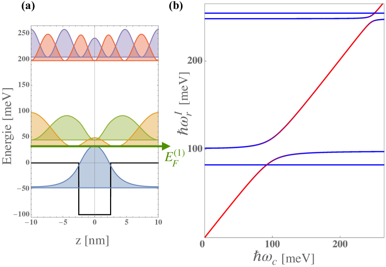
Let us start by studying a single quantum well whose potential barrier is and whose spatial width is , located at the middle of the semiconductor cavity spacer of length [Fig. 3(a)]. We set in order to have a single quantum confined state in the quantum well, followed by a quasi-continuum of states which are delocalized over the whole semiconductor region.
In Fig. 3(b) we present the polariton spectrum as a function of the cavity frequency . In order to maximize the light-matter coupling, we set [cf. panel (a)]. We can see that some “dark” states are completely uncoupled to the photonic mode, while the others show the typical anti-crossing behavior of polaritonic excitations Weisbuch et al. (1992); Liu (1997); Dini et al. (2003b). The region in which the polaritonic excitations manifests a hybrid light-matter nature is depicted in Fig. 3(b) via the color of the dispersion curve. The width of this region is proportional to the Rabi frequency .
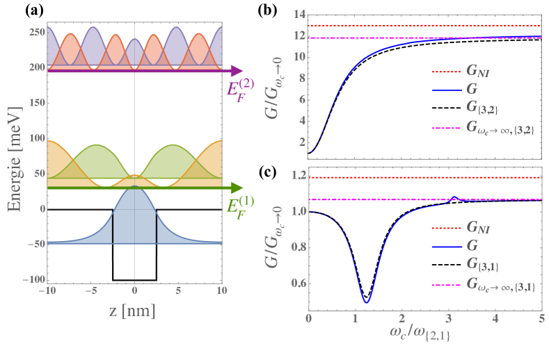
For the same configuration of Fig. 3, Fig. 4(b) and (c) show the cavity-embedded conductance normalized to as a function of the resonator frequency in two different configurations for the Fermi energy [see panel (a)]. We first consider an electronic density in such a way that the Fermi energy level is . In this configuration, the confined subband is maximally-populated without filling the delocalized subband. The blue curve of Fig. 4(c) represents the conductance, exhibiting sharp resonances while changing the cavity mode frequency. These features match the polaritonic resonances observed in Fig. 3(b) (coupled and transitions). At the main resonance, the conductance reduction is approximately . This effect is due to the scattering-time mixing [Eq. (28)].Note that the difference between and the noninteracting conductance (the dotted red line) is about a reduction coming from the competition of orbital and energetic effects. In this configuration, the energy subbands are sufficiently spaced for the two-subband approximation of Sec. III.3 to hold.The dashed black curve of Fig. 4(c) has been obtained considering the transition. As we can see, the two-subband approximation gives a good qualitative insight about the behavior of the conductance even if we miss the peak corresponding to the transition. The dot-dashed pink line represents the limit of equation (III.3) and shows how the light-matter coupling, even for a far-detuned cavity, renormalizes the conductance compared to the cavityless case. We note that the inequality (36) holds and that the cavity tends to reduce the effects of the depolarization shift with respect to the non-interacting case.
In Fig. 4(b), the Fermi Energy was fixed just below , in the continuum. Thus further transitions are allowed, giving significant contributions to the conductance. Here the depolarization shift reduces the conductance of almost one order of magnitude with respect to the non-interacting case. This large effect is smoothly weakened by the light-matter coupling when the cavity frequency is increased. We still can observe residual effects of resonances, but in this configuration the scattering-time mixing is much less relevant than the orbital and energetic effects. Remarkably, by increasing the cavity frequency the dark conductance increases by nearly an order of magnitude for the considered range of parameters. In panel (b), we also perform the two-subband approximation by restricting to the transition. Such approximation shows a good agreement, since the dashed black line matches well the blue curve.
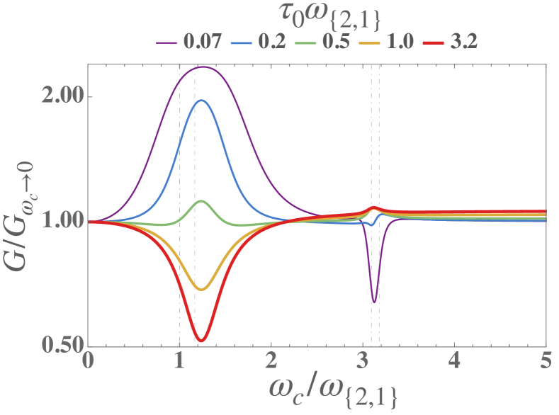
A critical parameter in determining the sign of the cavity-induced effects is the value of the Drude transport scattering time . To elucidate its role, we take the configuration of Fig. 3 and show in Fig. 5 the ratio for different values of . When we scan over the cavity frequency, the scattering times get a mixed light-matter nature around and, for , increases compared to the noninteracting case [see Eq. (28)]. According to Eq. (27), if the subband gives a contribution to the conductance , so that the conductance due to this transition decreases with respect to the cavity-less case. On the contrary when , the conductance is proportional to , which leads to an enhancement of the contribution of the transition.
IV.2 Multiple Quantum Wells

In view of experimental realizations, it can be more practical to consider larger cavity spacers. Increasing the cavity length decreases the light-matter interaction [cf. Eq. (9)]. However, this can be compensated by considering multiple quantum wells. For example, in Fig. 6(a) we represent the single-particle energy levels of a multiple quantum well heterostructure with a number of quantum wells. In Fig. 6(b) we consider different values of : for each case, we consider a cavity length nm and the Fermi energy is adjusted just below the quasi-continuum. All the confined subbands are approximately equally populated since the tunneling coupling between the different quantum wells is negligible. The results in Fig. 6(b) show the normalized conductance as a function of the cavity frequency for the different values of that we have considered. It is apparent that we observe a similar behavior while changing . Indeed, the collective coupling due to a succession of quantum wells approximately compensate the decrease of coupling due to the increase of the cavity length Dicke (1954); Bonifacio and Preparata (1970); Bonifacio et al. (1971); Laurent et al. (2015).
V Conclusions
In this work we have introduced a linear-response manybody formalism for the vertical conductance of an arbitrary n-doped parabolic semiconductor heterostructure. Within our formalism, it is possible to account for the effect of the light-matter coupling when such an heterostructure is embedded in a single-mode electromagnetic resonator in absence of illumination. We diagonalized the many-body Hamiltonian in the dipole gauge, accounting for the collective Coulomb interaction (depolarization shift) and the light-matter coupling in a bosonized formalism. As summarized by Eq. (17) and Eq. (18), the conductance is controlled by virtual transitions from the manybody ground state to the excited states via the collective current operator . The conductance depends on the matrix elements of the current operator between ground and polariton excited states, on the energy of such polariton excitations, and on the scattering times.
After presenting our general bosonized theory, we focused on the paradigmatic example of cavity-embedded quantum well heterostructures. We have shown that the cavity dark vertical conductance (no illumination) can be largely modified. This effect can be measured by observing the dependence of the conductance on the cavity mode frequency for a fixed cavity length . The hybridization of the scattering times leads to the appearance of resonances in the conductance as a function of the cavity frequency. These peaks can correspond to enhancement or suppression of the conductance depending on the value of the Drude electronic transport scattering time. Then we focused on the case of multiple quantum wells, showing that a similar phenomenology can be observed by using larger cavity lengths. Using parameters for -based semiconductor heterostructures, we have shown both qualitative effects (appearance of a multi-peak/dip structure) and quantitative effects (large enhancement or suppression). For a given quantum well structure, the largest vacuum effects are obtained when the Fermi energy lies above the quantum well barrier. As possible future developments of the present theory, we mention the case of dispersive multimode cavities and the investigation of the regime where the number of electrons is not large enough to allow for a bosonic treatment of the elementary excitations.
Our findings show the role of electromagnetic-vacuum effects on the vertical electronic transport of cavity-embedded semiconductor heterostructure. The flexibility of the formalism allows to generalize our theory on any kind of heterostructure, which is all the more significant since several devices are based on this technology. Among the possible generalizations, we mention the extension to systems with non-parabolic dispersions and band wave-mixing.
VI Acknowledgments
We thank A.D. Stone, R. Colombelli, J. Faist, C. Sirtori, G. Scalari, Y. Todorov for discussions.
Appendix A Hopfield-Bogoliubov matrix for the considered system
The Hopfield-Bogoliubov matrix associated with the Hamiltonian (5) can be written in the following block form:
| (37) |
with , and
When restricting to a single main transition of index , is a four by four matrix:
| (38) |
Appendix B Details about the linear-response formalism for the vertical nonlocal conductivity
In this Appendix we wish to show some intermediate steps of the derivation of Eqs. (17), (18), and (19) from a general linear-response function formalism. In the absence of external magnetic field and for an applied electric field applied along the growth direction , the current density variation in the sample is given by Bruus and Flensberg (2004)
| (39) |
The general nonlocal current-current response function reads
| (40) |
where is the -component of the paramagnetic current operator, namely
| (41) |
In the formalism of second quantization on the basis of non-interacting one-electron wave functions (1), the current density operator reads
| (42) |
Since the heterostructure is translationally invariant in the -plane, the application of a bias voltage along can only create a field . Similarly, the current variation can not depend on . We can thus integrate over the transverse surface both sides of Eq. (39) and get
| (43) |
The only dependence on and of Eq. (B) is in the current density operators. Hence, by introducing
| (44) |
the term in square brackets in Eq. (43) reads as of Eq. (18), and Eq. (43) becomes Eq. (17). Upon insertion of Eq. (42) into Eq. (44) one finally gets Eq. (19).
References
- Gendron et al. (2004) L. Gendron, M. Carras, A. Huynh, V. Ortiz, C. Koeniguer, and V. Berger, Applied Physics Letters 85, 2824 (2004).
- Jagadish et al. (2011) C. Jagadish, S. Gunapala, and D. Rhiger, Advances in infrared photodetectors, Vol. 84 (Elsevier, 2011).
- Faist et al. (1994) J. Faist, F. Capasso, D. L. Sivco, C. Sirtori, A. L. Hutchinson, and A. Y. Cho, Science 264, 553 (1994).
- Köhler et al. (2002) R. Köhler, A. Tredicucci, F. Beltram, H. E. Beere, E. H. Linfield, A. G. Davies, D. A. Ritchie, R. C. Iotti, and F. Rossi, Nature 417, 156 (2002).
- Levine et al. (1990) B. F. Levine, C. G. Bethea, G. Hasnain, V. O. Shen, E. Pelve, and R. R. Abbott, Applied Physics Letters 56, 851 (1990).
- Zussman et al. (1991) A. Zussman, B. F. Levine, and J. Kuo, J. M.and De Jong, Journal of Applied Physics 70, 5101 (1991).
- Liu et al. (1993) H. C. Liu, A. G. Steele, M. Buchanan, and Z. R. Wasilewski, Journal of Applied Physics 73, 2029 (1993).
- Levine (1993) B. F. Levine, Journal of Applied Physics 74, R1 (1993).
- Palaferri et al. (2018) D. Palaferri, Y. Todorov, A. Bigioli, A. Mottaghizadeh, D. Gacemi, A. Calabrese, A. Vasanelli, L. Li, A. G. Davies, E. H. Linfield, F. Kapsalidis, M. Beck, J. Faist, and C. Sirtori, Nature 556, 85 EP (2018).
- Orgiu et al. (2015) E. Orgiu, J. George, J. A. Hutchison, E. Devaux, J. F. Dayen, B. Doudin, F. Stellacci, C. Genet, J. Schachenmayer, C. Genes, G. Pupillo, P. Samorì, and T. W. Ebbesen, Nature Materials 14, 1123 (2015).
- Nagarajan et al. (2018) K. Nagarajan, J. George, A. Thomas, E. Devaux, T. Chervy, S. Azzini, J. Aziz, M. W. Hosseini, A. Kumar, C. Genet, and T. Ebbesen, preprint ChemRxiv:7498622 (2018).
- Paravicini-Bagliani et al. (2019) G. L. Paravicini-Bagliani, F. Appugliese, E. Richter, F. Valmorra, J. Keller, M. Beck, N. Bartolo, C. Rössler, T. Ihn, K. Ensslin, C. Ciuti, G. Scalari, and J. Faist, Nature Physics 15, 186 (2019).
- Schachenmayer et al. (2015) J. Schachenmayer, C. Genes, E. Tignone, and G. Pupillo, Phys. Rev. Lett. 114, 196403 (2015).
- Feist and Garcia-Vidal (2015) J. Feist and F. J. Garcia-Vidal, Phys. Rev. Lett. 114, 196402 (2015).
- Hagenmüller et al. (2017) D. Hagenmüller, J. Schachenmayer, S. Schütz, C. Genes, and G. Pupillo, Phys. Rev. Lett. 119, 223601 (2017).
- Bartolo and Ciuti (2018) N. Bartolo and C. Ciuti, Phys. Rev. B 98, 205301 (2018).
- Dini et al. (2003a) D. Dini, R. Köhler, A. Tredicucci, G. Biasiol, and L. Sorba, Phys. Rev. Lett. 90, 116401 (2003a).
- Ciuti et al. (2005) C. Ciuti, G. Bastard, and I. Carusotto, Phys. Rev. B 72, 115303 (2005).
- Anappara et al. (2009) A. A. Anappara, S. De Liberato, A. Tredicucci, C. Ciuti, G. Biasiol, L. Sorba, and F. Beltram, Phys. Rev. B 79, 201303 (2009).
- Günter et al. (2009) G. Günter, A. A. Anappara, J. Hees, A. Sell, G. Biasiol, L. Sorba, S. D. Liberato, C. Ciuti, A. Tredicucci, A. Leitenstorfer, and R. Huber, Nature 458, 178 (2009).
- Todorov et al. (2010) Y. Todorov, A. M. Andrews, R. Colombelli, S. De Liberato, C. Ciuti, P. Klang, G. Strasser, and C. Sirtori, Phys. Rev. Lett. 105, 196402 (2010).
- Bruus and Flensberg (2004) H. Bruus and K. Flensberg, Many-Body Quantum Theory in Condensed Matter Physics (Oxford, 2004).
- Babiker and Loudon (1983) M. Babiker and R. Loudon, Proceedings of the Royal Society A: Mathematical, Physical and Engineering Sciences 385, 439 (1983).
- Todorov and Sirtori (2012) Y. Todorov and C. Sirtori, Phys. Rev. B 85, 045304 (2012).
- De Bernardis et al. (2018) D. De Bernardis, P. Pilar, T. Jaako, S. De Liberato, and P. Rabl, Phys. Rev. A 98, 053819 (2018).
- Cortese et al. (2019) E. Cortese, I. Carusotto, R. Colombelli, and S. D. Liberato, Optica 6, 354 (2019).
- Lee et al. (2010) B. Lee, I.-M. Lee, S. Kim, D.-H. Oh, and L. Hesselink, Journal of Modern Optics 57, 1479 (2010).
- Todorov and Sirtori (2014) Y. Todorov and C. Sirtori, Phys. Rev. X 4, 1031 (2014).
- Paulillo et al. (2014) B. Paulillo, J. M. Manceau, A. Degiron, N. Zerounian, G. Beaudoin, I. Sagnes, and R. Colombelli, Opt. Express 22, 21302 (2014).
- Paulillo et al. (2017) B. Paulillo, S. Pirotta, H. Nong, P. Crozat, S. Guilet, G. Xu, S. Dhillon, L. H. Li, A. G. Davies, E. H. Linfield, and R. Colombelli, Optica 4, 1451 (2017).
- Klingshirn (2007) C. Klingshirn, Semiconductor Optics, Advanced texts in physics (Springer Berlin Heidelberg, 2007).
- Note (1) For simplicity, we neglect here the variation of effective mass along the heterostructure.
- De Liberato and Ciuti (2009) S. De Liberato and C. Ciuti, Phys. Rev. Lett. 102, 136403 (2009).
- Note (2) More specifically, with the population operator in subband and . As long as one considers states with a total number of excitations much smaller than , one has De Liberato and Ciuti (2009) . This implies that within a few-excitation subspace one can consider .
- Note (3) This can be done by projecting the full electronic Hamiltonian over the manybody excited states Todorov and Sirtori (2012); De Liberato (2009).
- Lee and Galbraith (1999) S.-C. Lee and I. Galbraith, Phys. Rev. B 59, 15796 (1999).
- De Liberato and Ciuti (2012) S. De Liberato and C. Ciuti, Phys. Rev. B 85, 125302 (2012).
- Hopfield (1958) J. J. Hopfield, Phys. Rev. 112, 1555 (1958).
- Nataf and Ciuti (2010) P. Nataf and C. Ciuti, Nature communications 1, 72 (2010).
- Girvin and Yang (2019) S. M. Girvin and K. Yang, Modern Condensed Matter Physics (Cambridge University Press, 2019).
- Allen (2006) P. B. Allen, Conceptual Foundations of Materials: A Standard Model for Ground- and Excited-State Properties, edited by S. Louie and M. Cohen, Contemporary Concepts of Condensed Matter Science (Elsevier Science, 2006).
- Baranger and Stone (1989) H. U. Baranger and A. D. Stone, Phys. Rev. B 40, 8169 (1989).
- Kane et al. (1988) C. L. Kane, R. A. Serota, and P. A. Lee, Phys. Rev. B 37, 6701 (1988).
- Weisbuch et al. (1992) C. Weisbuch, M. Nishioka, A. Ishikawa, and Y. Arakawa, Phys. Rev. Lett. 69, 3314 (1992).
- Liu (1997) A. Liu, Phys. Rev. B 55, 7101 (1997).
- Dini et al. (2003b) D. Dini, R. Köhler, A. Tredicucci, G. Biasiol, and L. Sorba, Phys. Rev. Lett. 90, 116401 (2003b).
- Dicke (1954) R. H. Dicke, Phys. Rev. 93, 99 (1954).
- Bonifacio and Preparata (1970) R. Bonifacio and G. Preparata, Phys. Rev. A 2, 336 (1970).
- Bonifacio et al. (1971) R. Bonifacio, P. Schwendimann, and F. Haake, Phys. Rev. A 4, 302 (1971).
- Laurent et al. (2015) T. Laurent, Y. Todorov, A. Vasanelli, A. Delteil, C. Sirtori, I. Sagnes, and G. Beaudoin, Phys. Rev. Lett. 115, 187402 (2015).
- De Liberato (2009) S. De Liberato, Cavity quantum electrodynamics and intersubband polaritonics of a two dimensional electron gas, Theses, Université Paris-Diderot - Paris VII (2009).