Patterning of diamond with 10 nm resolution by electron-beam-induced etching
Abstract
We report on mask-less, high resolution etching of diamond surfaces, featuring sizes down to 10 nm. We use a scanning electron microscope (SEM) together with water vapor, which was injected by a needle directly onto the sample surface. Using this versatile and low-damage technique, trenches with different depths were etched. Cross sections of each trench were obtained by focused ion beam milling and used to calculate the achieved aspect ratios. The developed technique opens up the possibility of mask- and resist-less patterning of diamond for nano-optical and electronic applications.
-
March 2019
Keywords: Diamond, gas-assisted etching, nanostructuring, patterning
1 Introduction
Diamond is a material that possesses unique and attractive properties including ultrahigh hardness, chemical stability and mechanical strength, while it is highly transparent and an exceptional thermal conductor[1]. Furthermore, diamond is a wide-bandgap semiconductor with working temperatures up to 500. It has a bandgap of 5.47 eV at room temperature and its surface can be functionalized to exhibit negative electron affinity. Due to these physical properties in combination with the capability of hosting nitrogen vacancy luminescence centers (NV), diamond is one of the most promising candidates as a platform for next generation sensing, nanophotonic and quantum information devices[2, 1].
The processing of diamond for its implementation in functional devices is, however, extremely challenging due to the very same physical properties that render it an excellent candidate for these applications. Currently, high resolution diamond structuring requires arduous masking techniques and ion bombardment[3, 4] or high power laser ablation[5], which often cause damage and material re-deposition artifacts[6, 7] At present, the prevailing method for the mask-less patterning of diamond is Focused Ion Beam (FIB) milling, which however limits the fabrication process due to extended surface damage that leads to graphitization, re-deposition of carbon, ion implantation and low resolution. [8, 3]
As a less-destructive patterning technique of diamond layers, gas-assisted Electron Beam Induced Etching (EBIE)[9, 10] was proposed, which is a well-known technique being used for high resolution patterning of semiconductors such as GaAs[11] and Ge[12] as well as graphene[13]. Gas assisted EBIE to pattern diamond was first proposed by Taniguchi et al.[14] and we show here that is an alternative, low-damage method that opens the way for mask-less patterning of diamond for nanoscale optoelectronic applications without the need of the FIB. This method is based on the combination of an electron beam from a Scanning Electron Microscope (SEM) and in-situ exposure to a suitable gaseous etchant. Common etchants are oxygen[14], hydrogen[15] and water vapor[16]. The working principle behind this method is that the electron beam ionizes the gas molecules, which then create volatile compounds with the carbon atoms on the diamond surface[17, 18, 15]. After the first reports on the method[14, 15], further work has been published, studying the effect of different gases and pressure [16, 19] on the etching process. More recently, the patterns that are being created on the surface of diamond during etching were studied in correlation with the gases used in each case [18, 20]. However, the method was not studied until now in terms of high resolution in the range of nanometers for direct 3D, mask-less device nano-fabrication on the surface of diamond. The best resolution reported so far on single crystalline diamond was nm [6]. In this work, we report the mask-less and high resolution patterning of hydrogen-terminated single crystalline diamond samples using water vapor assisted EBIE featuring sizes down to 10 nm.
2 Sample synthesis and experimental setup
2.1 Sample synthesis
The samples were grown in a microwave plasma-assisted CVD reactor based on a 2.45 GHz IPLAS CYRANNUS I-6” plasma source[21]. The single-crystal, {100}-oriented diamond samples were placed on the substrate holder and the chamber was pumped down to mbar. Then a hydrogen plasma at 200 mbar, with a microwave power of 2.6 kW and a gas flow of 400 sccm for 45 min was used to clean the sample and sample holder prior to deposition. The deposition started at 120 mbar chamber pressure, with 1.26 kW microwave power. The flow was at 500 sccm with a purity of 7.0, while for methane was 57 sccm with a purity of 9.0 and a substrate temperature of 810. Deposition took 6 hours, resulting in an approximately 17 m thin film with {100} orientation. These surfaces were used for the etching experiments as grown.
2.2 Experimental setup
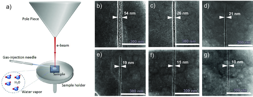
For the EBIE, a FEI Helios 600 NanoLab DualBeam setup was used, which integrates an electron and an ion beam. This system implements a gas injection system (GIS) for enhanced etching and material removal, as well as metal and insulator deposition. For the purpose of our study, only the electron beam was utilized in combination with simultaneous injection of water vapor using a GIS needle in an Ultra-High Vacuum (UHV) environment of mbar. The water is supplied in the form of Magnesium Sulfate Heptahydrate (), which -upon heating- releases water in gaseous form. Water vapor is released locally above the sample using a needle that is inserted a few m above the sample surface. The working principle that governs the gas-assisted EBIE method, as presented in Fig.1, is based on the dissociation of water vapor molecules due to impact ionization from the electrons. The resulting ions then create volatile compounds with the carbon atoms of the diamond surface (volatilization), which are then removed from the sample and eventually pumped out of the chamber[15]. Subsequently, as described in the second part of the results section, the utilization of the focused ion beam is necessary in order to mill a rectangular area across each trench, to obtain the corresponding cross section and measure the depth of each trench for the calculation of the aspect ratio. For this step, the stage is tilted by 52 degrees. The focused ion beam consists of ions derived from a Liquid Metal Ion Source (LMIS) source.
3 Results
3.1 High resolution parametric study
In order to achieve the highest resolution of 10 nm and the aspect ratio of 4.5 the influence of the e-beam acceleration voltage and current on the etching process was investigated. It was found that the hydrogen-termination of the diamond samples is crucial for our study because it provides sufficient surface conductivity. Due to the two-dimensional hole gas (2DHG) that is established on the surface of the sample[22], charging effects can be avoided and thus, high-resolution imaging and patterning can be achieved.
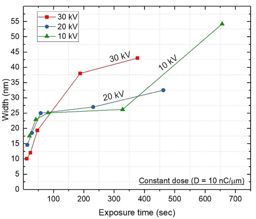
The single crystalline diamond sample was mounted on the sample holder, inserted in the FIB setup chamber and the system was pumped down to UHV region of mbar. For the trench series, the Ultra High Resolution mode (Immersion) was implemented with the Through The Lens (TTL) detector. Using this mode, trenches of 1 m length and only a few nm width were patterned into the diamond surface with varying electron beam current and acceleration voltage and the corresponding trench width was measured in each case. The dose of the e-beam was kept constant for every patterned trench in order to compare the effect of different SEM parameters on the etching process. Note that under constant dose the variation of the beam current, lead to different exposure times to the water vapor and the e-beam.
As shown in Fig.2, an increase of the current of the electron beam corresponds to reduction of the exposure and etching time, which results to better resolution of the patterned trenches. This indicates that the resolution is given by the temporal stability of the setup. The lowest acceleration voltage of 10 kV and a small current value of 43 pA for 11 minutes, yield a resolution of 54 nm, while increased current and voltage to 0.69 nA and 30 kV for 12 seconds respectively yields trenches of only 10 nm. For short exposure times, i.e. below 60 seconds, the acceleration voltage of 30 kV provides better resolution compared to 20 and 10 kV. However, for longer exposure times, 30 kV of acceleration voltage lead to broader trenches than the 10 and 20 kV.
3.2 Aspect ratio
In the second part of this study, taking into account the results presented in the previous section and using the beam current that resulted in the best resolution trenches (0.69 nA), a second series of trenches was patterned. The current of the electron beam was kept at 0.69 nA, while the exposure time was increasing from 2 minutes to 5, 15, 30 and 45 minutes and the e-beam dose was calculated respectively. The linear distribution of the e-beam for the aforementioned exposure times correspond to 0.08, 0.2, 0.62, 1.24 and 1.86 C/m. The increase of the dose resulted in deeper trenches, however, with increased widths. This effect was investigated by calculating the aspect ratio of each trench.
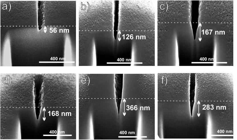
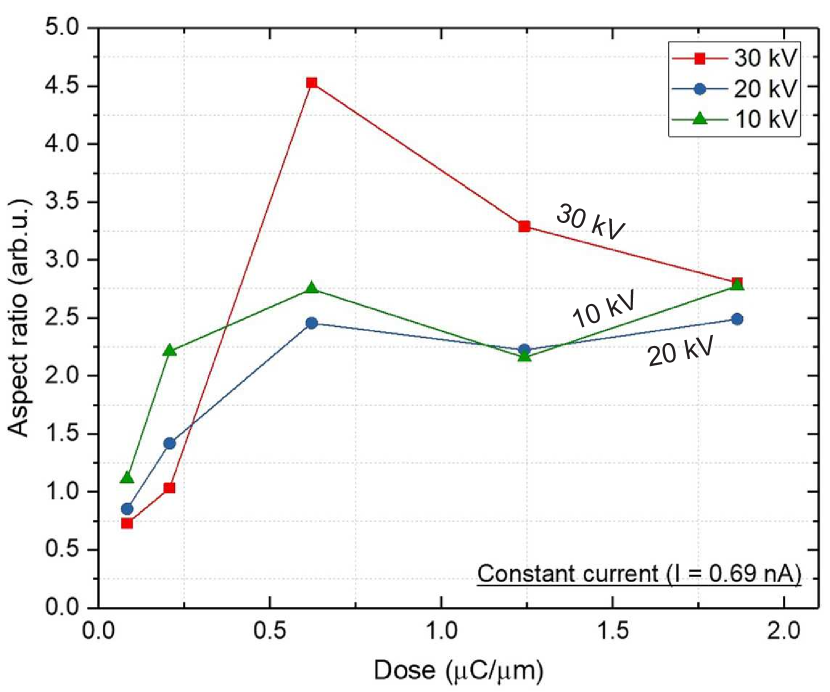
For a stable current value of 0.69 nA and acceleration voltages of 10, 20 and 30 kV, 15 trenches were patterned in total for 2,5, 15, 30 and 45 minutes of exposure time. The trench widths were measured and then the stage was tilted to in order to employ the FIB to mill rectangular holes of 600x600 nm to 1 m depth and measure the cross section of the trenches, see Fig.3. Using the measured widths and cross sections, the aspect ratios for the different acceleration voltages were calculated and are presented in Fig.4. The obtained aspect ratios are calculated to be between 1:1 and 1:5.
For small exposure times (5 and 15 min) the aspect ratio is around 1:1, while with increasing the exposure time, the depth of the trenches is increased up to 385 nm. However, by increasing the exposure time, a broadening is also observed in most trenches. This effect is attributed to increased number of passes in combination with a minor sample drift and external vibrations. The broadening resulted in increased widths and an asymmetry of trenches that lead to variations of the aspect ratios despite the increased depths. It is noteworthy, that the broadening of the trenches is not completely avoidable even if the drift is reduced. A possible reason for this is that the water molecules that are being adsorbed from a larger area around the etched trench, can also be dissociated by the secondary electrons created under the diamond surface. This could explain the reversed conical shape of the trenches that can be seen at Fig.3. The latter effect of the cone-shaped broadened trenches should be also attributed to the reduced diffusion of the water molecules in the trench during etching process. Under the conditions maintained during etching (), the fluid dynamics are described by the free molecular flow. As a consequence, the random movement of the water molecules inhibits their further diffusion in the etched trench, thus reducing the thickness gradually.
4 Conclusion
In conclusion, we have studied in depth the EBIE method on diamond. By systematically varying the etching parameters, we were able to obtain an exceptionally high resolution of only 10 nm for patterned trenches. The influence of the different parameters on the etching process was investigated in depth and defined accurately. Furthermore, the aspect ratio of the patterned trenches was calculated, in order to obtain an estimate about the removed material. Apart from the optimum choice of the etching parameters, the hydrogen termination of the diamond samples was of great importance to reach high resolution imaging and patterning, because it provided the necessary surface conductivity that minimized the charging effects. The reported results can be improved even further by reducing the number of e-beam passes over the patterned area, which will limit the observed broadening. Our results open up new ways of easier processing of diamond towards the fabrication of high precision devices at the nanometer range that exploit the unique properties of this special material.
5 Acknowledgments
This work was financially supported by the International Max Planck Research School for Interface Controlled Materials for Energy Conversion (IMPRS-SurMat).
6 References
References
- [1] Lončar M and Faraon A 2013 MRS Bulletin 38 144–148 ISSN 08837694
- [2] Aharonovich I and Neu E 2014 Advanced Optical Materials 2 911–928 ISSN 21951071 (Preprint 1408.5451)
- [3] Bayn I, Bolker A, Cytermann C, Meyler B, Richter V, Salzman J and Kalish R 2011 Applied Physics Letters 99 183109 ISSN 00036951
- [4] Taniguchi J 2002 Journal of Vacuum Science & Technology B: Microelectronics and Nanometer Structures 16 2506 ISSN 0734211X
- [5] Lehmann A, Bradac C and Mildren R P 2014 Nature Communications 5 ISSN 20411723
- [6] Martin A A, Toth M and Aharonovich I 2014 Scientific Reports 4 2–5 ISSN 20452322 (Preprint 1403.4067)
- [7] Bayn I, Meyler B, Salzman J and Kalish R 2013 Triangular nanobeam photonic cavities in single- crystal diamond p CThZ7
- [8] Uzan-Saguy C, Cytermann C, Brener R, Richter V, Shaanan M and Kalish R 1995 Applied Physics Letters 67 1194 ISSN 00036951
- [9] Randolph S J, Fowlkes J D and Rack P D 2006 Critical Reviews in Solid State and Materials Sciences 31 55–89 ISSN 10408436
- [10] Hoffmann P 2005 Proceedings of SPIE 5925 592506–592506–15 ISSN 0277786X
- [11] Ganczarczyk A, Geller M and Lorke A 2011 Nanotechnology 22 ISSN 09574484
- [12] Gökdeniz Z, Wanzenboeck H, Shawrav M, Bertagnolli E, Taus P, Mika J and Waid S 2015 Materials Science in Semiconductor Processing 42 170–173 ISSN 13698001
- [13] Sommer B, Sonntag J, Ganczarczyk A, Braam D, Prinz G, Lorke A and Geller M 2014 Electron-beam induced nano-etching of suspended graphene
- [14] Taniguchi J, Miyamoto I, Ohno N and Honda S 1996 Electron Beam Assisted Chemical Etching of Single Crystal Diamond Substrates
- [15] Taniguchi J, Miyamoto I, Ohno N, Kantani K, KoMURO M and Hiroshima H 1997 Electron beam assisted chemical etching of single-crystal diamond substrates with hydrogen gas
- [16] Niitsuma J I, Yuan X L, Koizumi S and Sekiguchi T 2006 Japanese Journal of Applied Physics, Part 2: Letters 45 71–73 ISSN 00214922
- [17] Martin A A, Phillips M R and Toth M 2013 ACS Applied Materials and Interfaces 5 8002–8007 ISSN 19448244
- [18] Martin A A, Bahm A, Bishop J, Aharonovich I and Toth M 2015 Physical Review Letters 115 1–5 ISSN 10797114
- [19] Martin A A, McCredie G and Toth M 2015 Applied Physics Letters 107 ISSN 00036951
- [20] Bishop J, Fronzi M, Elbadawi C, Nikam V, Pritchard J, Fröch J E, Duong N M H, Ford M J, Aharonovich I, Lobo C J and Toth M 2018 ACS Nano 12 2873–2882 ISSN 1936086X
- [21] Aschermann B and Spitzl R DEVICE FOR THE PRODUCTION OF PLASMAS BY MICROWAVES EP0872164
- [22] Maier F, Riedel M, Mantel B, Ristein J and Ley L 2000 Origin of Surface Conductivity in Diamond