Electronic, magnetic, and optical properties of Mn-doped GaSb: a first-principles study
Abstract
Half-metallic ferromagnets can produce fully spin-polarized conduction electrons and can be applied to fabricate spintronic devices. Thus, in this study, the electronic structure, magnetic properties, and optical properties of GaSb, which has exhibited half-metallicity, doped with Mn, a 3d transition metal, are calculated using the generalized gradient approximation and Heyd-Scuseria-Ernzerhof (HSE) functional. Ga1-xMnxSb () materials exhibit ferromagnetic half-metallic properties and a high Curie temperature, indicating that this series can applied in spintronic devices. Meanwhile, they absorb strongly in the infrared band, suggesting that Ga1-xMnxSb also has potential applications in infrared photoelectric devices.
Introduction
Over the past few decades, spintronics has developed rapidly. Compared with traditional semiconductor devices, spintronic devices have the advantages of storage non-volatility, lower power consumption, higher integration, etc. Prinz (1998); Ohno et al. (1992). In 1983, through their study of alloys such as Heusler alloys NiMnSb and PtMnSb, Groot et al. first discovered a material with a special energy band structure in which one direction of the electron spin band exhibits metallicity, while the other direction of the electron spin band is semiconducting. They thus named the material a half-metallic ferromagnet (HMF) De Groot et al. (1983); Chen and Ren (2013). This type of material can produce fully spin-polarized conduction electrons, a good source of spin-flow injection Watts et al. (2000); Xie and Liu (2004); Doumi et al. (2015), With their magnetic moment quantization and zero magnetic susceptibility, HMFs can be used to fabricate spintronic devices such as spin diodes, spin field effect transistors, spin valves, and spin filters Wolf et al. (2001); Pickett and Moodera (2001); Osborne (2001); Awschalom and Kikkawa (1999). Thus, not only will HMFs play an important role in a new generation of high-performance microelectronic devices but they will also open up new avenues in the research of polarization transport theory and spintronics Žutić, Fabian, and Sarma (2004); Katsnelson et al. (2008); Chadov et al. (2011); Alijani et al. (2011).
Unlike conventional electronics, spintronics utilizes the charge and spin of electrons to carry information and, thus, has superior performance. During the development of spintronic materials, new magnetic materials with both magnetic and semiconductor properties have been discovered, which has aroused great interest in the study of spintronics. Binary semiconductors doped with magnetic transition metal elements have also played an important role in spintronics development. Related research has found that a small number of magnetic elements can be incorporated into semiconductors such as Group II-VI, Group IV, or Group III-V elements Coey (2005); Yang et al. (2010); Katayama-Yoshida and Sato (2003). In such systems, the incorporated magnetic atoms replace the cations or anions in the semiconductor unit cell, or defects form in the system, both of which have led to the discovery of many new spintronic materials. Investigations have revealed that III-V compound semiconductor materials have broad applications in optoelectronic devices, optoelectronic integration, ultrahigh-speed microelectronic devices and ultrahigh-frequency microwave devices and circuits Hass and Henvis (1962); Ehrenreich (1961).
In recent years, many new half-metallic (HM) materials have been discovered by doping III-V binary semiconductors with transition metal elements Liu and Liu (2007); Noor, Ali, and Shaukat (2011); Rahman, Cho, and Hong (2010); Shirai (2001). However, few studies exist in the literature on the electronic properties of the III-V semiconductor material GaSb doped with 3d transition metals. GaSb is a direct band gap semiconductor with a zinc-blende (ZB) crystal structure, a band gap of about 0.72 eV, and a lattice constant of 0.61 nm Milnes and Polyakov (1993), GaSb has the characteristics of high electron mobility, high frequency and low threshold, and a high photoelectric conversion rate Zhang and Callaway (1969); Ahmed et al. (2009); Schottky and Bever (1958). Meanwhile, the lattice constant of this material approximately matches those of other various ternary and quaternary III-V compound semiconductor materials, which can greatly mitigate the problematic stress and defects caused by lattice mismatch. Thus, GaSb has become an important substrate material for preparing long-wave light-emitting diodes (LEDs), photodetectors, and fiber-optic communication devices Bennett and Soref (1987); Aspnes and Studna (1983); Wei et al. (2002). Nonetheless, to the best of our knowledge, GaSb doped with the transition metal Mn has never been systematically researched about Kondrin et al. (2008); Seña et al. (2016); Galanakis and Mavropoulos (2003); Ahmad and Amin (2013). In this paper, we report first-principles calculations of Ga1-xMnxSb () compounds, which are observed to be HMFs and, thus, could be useful in both spintronics and infrared photoelectrics.
The remaining part of the paper is organized as follows: in Section II, we present our calculations in detail; in Section III, we describe the results and discuss the electronic, magnetic, and optical properties of these ZB ternary Ga1-xMnxSb compounds. Finally, in Section IV, we summarize our results.
Methods
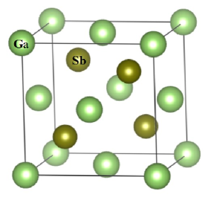
GaSb has the ZB crystal structure, and its space group is (No. 216) Dresselhaus (1955); Cohen and Bergstresser (1966). Each Ga (Sb) atom is at the center of a tetrahedron of its four nearest-neighbor Sb (Ga) atoms, as shown in Fig.1. For the calculations, we replace either one, two, or three Ga atoms with Mn atoms in the GaSb unit cell, for a Mn doping ratio of , , and , respectively. Thus, we obtain a series of ZB Ga1-xMnxSb () compounds. The main contents of this paper are the study of the electrical, magnetic, and optical properties of ZB Ga1-xMnxSb () by first principles.
All calculations were performed using the first-principles calculation package VASP (Vienna ab initio simulation package) Kresse and Hafner (1993); Kresse and Furthmüller (1996a). For the simulation, we chose the projected augmented wave (PAW) Kresse and Joubert (1999) to describe the interaction between electrons and nuclei. The correlation between electrons and electrons uses a generalized gradient (generalized gradient approximation, GGA) Perdew et al. (1992) in the form of the Perdew-Burke-Ernzerhof functional (PBE-96) Perdew, Burke, and Ernzerhof (1996a). First, we optimize the Monkhorst-Pack special K-point selection for the plane wave truncation energy and the Brillouin zone integral for each structural system. Ecut is set to 400 eV, and the K point is . In the crystal structure optimization and atomic relaxation process, the accuracies of the total energy convergence of the system and the force convergence on a single atom are eV and eV/atom, respectively.
We calculated the total energy of non-magnetic (NM), ferromagnetic (FM), and antiferromagnetic (AFM) states of ZB Ga1-xMnxSb () as a function of the lattice constant. Because the PBE functional calculation underestimates the crystal band gap, we added the Heyd-Scuseria-Ernzerhof (HSE) hybrid density functional Batista et al. (2006); Heyd, Scuseria, and Ernzerhof (2003) to calculate the electron band. HSE is used to solve the numerical analysis of the Kohn-Sham Kohn and Sham (1965) equation in the plane wave basis set and introduces the non-local exact exchange. Some of this equation is calculated by a precise exchange, thus, improving the electron self-interaction of the system. The total energy of the electronic system can be described well by HSE, and the calculated energy band is similar to that observed experimentally. Thus, the calculation results are reasonable.
Results and Discussions
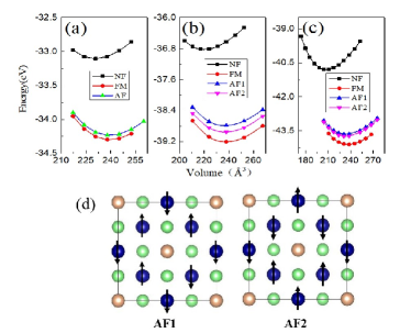
Magnetic properties. We calculated the electronic ground state properties of Ga1-xMnxSb materials at different Mn concentrations. As Fig. 2(d) shows, the FM and AFM states are calculated mainly by making the spins of the even-numbered Mn parallel, anti-parallel, and cross-parallel. Figure 2(a), 2(b) and 2(c) show the energy Cvolume curves corresponding to the three different magnetic states (NM, FM, AFM, respectively) of the Ga1-xMnxSb at different Mn concentrations. The figure demonstrates that the FM state has the lowest energy in all three states. Therefore, for equilibrium lattice constant, the FM state of ZB Ga1-xMnxSb is the most stable.
| x | Mtot/NMn () | MMn () | MSb () | GP | TC | MP |
|---|---|---|---|---|---|---|
| 0.25 | 4 | 3.831 | -0.075 | FM | 496 | HMF |
| 0.5 | 4 | 3.918 | -0.124 | FM | 866 | HMF |
| 0.75 | 4 | 3.889 | -0.156 | FM | 919 | HMF |
| 1 | 4 Zheng and Davenport (2004) | - | - | FM | 587 Popova et al. (2006) | HMF |
In their equilibrium lattice constants, the Ga1-xMnxSb () compounds have an integer magnetic moment (in a Bohr magnet, ), corresponding to the FM HM nature. The average magnetic moment of a single Mn atom in Ga1-xMnxSb () is 4.0 . Fig.3 shows the total magnetic moment of these three FM HM materials, which varies with the lattice constant within . The total magnetic moment remained constant for lattice changes between and . Additionally, we explored the magnetic moment contribution of each atom in the material. The total magnetic moment is dominated by the magnetic moment of the Mn- orbital, and the contributions of other atomic magnetic moments are small. Furthermore, the contributions of the Mn- and Sb- orbital magnetic moments are opposite each other. Fig.3 demonstrates that the magnetic moment changes of Mn- increase with the increasing lattice constant, but this trend is gradual. Table I lists the magnetic moments and material properties of each atom. Next, we estimate the Curie temperature of the three FM half-metals using the mean field method Cheng et al. (2013); Fukushima et al. (2004); Şaşıoğlu, Sandratskii, and Bruno (2004),
| (1) |
where C represents the number of doped Mn atoms in the unit cell, and represents the Boltzmann constant. All three compounds are found to have a Curie temperature above 400 K at room temperature. MnSb has been proven to be a FM half-metal with a Curie temperature of 587 K Popova et al. (2006). Table I shows the magnetic properties and Curie temperature of Ga1-xMnxSb ().
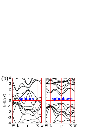
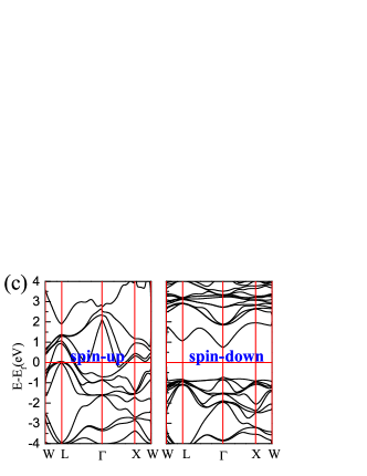
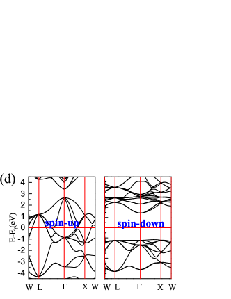
Electronic properties. Fig.4 gives the energy band structures of Ga1-xMnxSb () compounds at their equilibrium lattice constants. The spin-up energy bands of Ga1-xMnxSb () straddle the Fermi level EF, which is metallic, while the spin-down energy band has a gap, which indicates insulator behavior. Ga1-xMnxSb has a conduction band bottom and a valence band top located at the high symmetry point of the Brillouin zone, which is a direct band gap, and the band gap becomes wider as the Mn concentration increases, as shown in Table I. Therefore, the different characteristics exhibited by the spin-up and spin-down electron energy bands reveal that the ZB Ga1-xMnxSb crystal has HM properties. We also used the same method to calculate the electronic structure of ZB GaSb and ZB MnSb by completely replacing Ga atoms, and we obtained the band diagram of the semiconductor GaSb with the direct band gap at the center of the Brillouin zone. MnSb is a FM half-metal, as shown in Fig.4(d), which agree with previous results. These two crystalline materials have long been studied, and our results are consistent with the electronic structures reported in the previous literature Cohen and Bergstresser (1966); Zheng and Davenport (2004). By comparison, we found that the FM HM properties of Ga1-xMnxSb () are caused by Mn atoms.
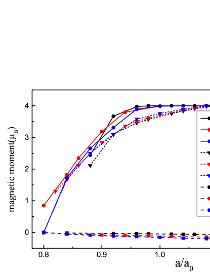
Table II shows the equilibrium lattice constants and ground state properties calculated for Ga1-xMnxSb () and related values from the literature. We determined that the Ga-Sb bond is 2.638 long when the semiconductor GaSb is for the equilibrium lattice constant. By comparing the bond lengths among the atoms in the series of FM Ga1-xMnxSb () shown in Table II, we can see that after doping with Mn, the outermost orbital electrons of Mn in Ga1-xMnxSb () are consumed by the bond owing to the difference in electronegativity and the electron orbital interatomic hybridization. Because a larger Ga atom is substituted with a smaller Mn atom, the Mn-Sb bonds in the ZB structure are shorter than the Ga-Sb bonds. Table II demonstrates that the semiconductor band gap and the HM gap of HMF Ga1-xMnxSb () both increase with increasing concentration. The minimum of the HM gap of a HM material is intermediate along the distance from the Fermi energy to either the valence band or the bottom of conduction band in the spin sub-band with a band gap Zheng et al. (2008).

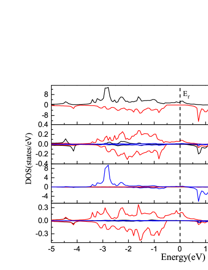
To further study the principle underlying the HM properties of this series of HMF materials, the total density of states of Ga0.75Mn0.25Sb is selected because the electronic densities of the Ga1-xMnxSb () compounds are similar. Additionally, the atomic wave partial density of states is taken as an example. As Fig. 5 shows, the total electronic density of Ga0.75Mn0.25Sb is metallic in the spin state near the Fermi surface, while the lower spin state has a clear band gap, indicating semiconductivity. Since only one spin-oriented electron exists at the Fermi level of Ga0.75Mn0.25Sb, the spin polarizability is defined as Chadov et al. (2011); Alijani et al. (2011).
| (2) |
where and are the spin-up and spin-down density of states, respectively. We can conclude that the spin polarization of the conduction electrons of Ga0.75Mn0.25Sb is .
Because the electromagnetic and optical properties of most materials are derived from the intermetallic orbital , , and electron orbital hybridization, these properties are related to the electronic configuration of each atom and the electron orbital hybridization between atoms De Paiva, Nogueira, and Alves (2004); Chen, Xu, and Gao (2013); Arif, Ahmad, and Amin (2012); Nabi et al. (2017). Because the valence electronic configuration of Mn is , and the valence electron configuration of Ga is , the outermost orbit has only one electron in Ga. Additionally, the valence electron configuration of Sb is , and its state has three electrons, which is the half-filled state (-state full-shell layer is six electrons). Furthermore, comparing the bond length and density of states between individual atoms in the crystal suggests that strong hybridization occurs near the Fermi level. As Table II shows, the Mn-Sb bond length are shorter than that of the the Ga-Sb, indicating that the electron hybridization occurs mainly between the transition metal atom Mn and the Sb atom. The orbital of Mn and the orbital of Sb are found to undergo pd electron hybridization; therefore, the electronic density distribution of Mn exhibits a shift in the energy level. In other words, electron orbital hybridization causes the total electronic density of crystal materials to redistribute, which is the main reason Ga1-xMnxSb () exhibits FM HM properties.
Optical Properties. The optical properties of a solid can be described by a dielectric function Perdew, Burke, and Ernzerhof (1996b); Kresse and Furthmüller (1996b), which consists of a real part and an imaginary part and is defined as
| (3) |
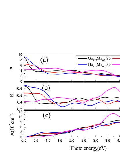
Because Ga1-xMnxSb () belongs to the cubic system, its optical properties are known to be isotropic. In this study, the dielectric constant of Ga1-xMnxSb () is calculated, and the optical properties are analyzed. Fig.6 shows the relationship between the optical properties and the incident light energy, comparing the refractive index n, reflectance R, and absorption coefficient A of some crystalline materials. We can use the real and imaginary parts of the dielectric function to obtain the absorption coefficient and reflectivity of the solid using the following formulas:
| (4) |
| (5) |
| a0 | LMS | LGS | EHM-HSE | EHM-PBE | EHSE | EPBE | |
|---|---|---|---|---|---|---|---|
| 0 | 6.095 | - | 2.554 | - | - | 0.526 | 0.083 |
| 0.720 Kim et al. (2010) | 0.110 Kim et al. (2010) | ||||||
| 0.25 | 6.208 | 2.663 | 2.697 | 0.144 | 0.086 | 1.239 | 0.593 |
| 0.5 | 6.315 | 2.678 | 2.689 | 0.405 | - | 1.260 | 0.452 |
| 0.75 | 6.179 | 2.671 | 2.696 | 0.723 | - | 1.455 | 0.746 |
| 1 | 6.178 | 2.675 | - | 0.988 | - | 2.217 | 1.457 |
| 6.166 Guo and Liu (2011) | 0.200 Guo and Liu (2011) | 1.491 Guo and Liu (2011) | |||||
| 6.166 Shi and Liu (2005) | 0.150 Shi and Liu (2005) | 0.900 Shi and Liu (2005) |
Fig6(a) and 6(b) reveal that the static refractive index n(0)=9 of Ga0.75Mn0.25Sb and the static reflectance are R(0)=0.64, respectively, which are higher than those of GaSb, i.e., n(0)=4.6 and R(0)=0.41, respectively. The calculation results revealed that the static refractive index and static reflectivity of Mn-doped FM materials are higher than those of GaSb. The refraction spectrum of Ga1-xMnxSb () in Fig. 6(a) demonstrates that in the energy range of eV, the refractive indices of these materials tend to decrease gradually with the increasing incident light energy, whereas they decrease rapidly in the energy range of visible light at eV. Furthermore, the refractive power of the material for infrared light is much higher than that for ultraviolet light, and the static refractive index and the static reflectivity of the doped material are both higher than those of undoped GaSb. The reflection and refraction patterns of different Mn concentrations demonstrate that the variations in the refractive index and reflectivity are similar when doping is not higher than , and the higher the doping concentration is, the more obviously the refractive index changes. Fig.6(c) reveals that in the energy range of eV, the absorption coefficients of the four Ga1-xMnxSb compounds tend to increase gradually. In the visible region, there is no obvious absorption peak, and the absorption coefficient of the material does not change much after doping with Mn. In contrast, in the infrared region, that is, when the incident photon energy below 1.3 eV, the effects of doping are obvious. The doped material absorbs significantly more infrared light than GaSb. Therefore, Ga1-xMnxSb () has a strong absorption capacity for infrared light and is suitable for use in electronic devices related to infrared detection.
This paper presents the electronic structure and the magnetic and optical properties of Mn-doped semiconductor GaSb studied using a first-principles calculation method. The spin-polarized electronic density of states of Ga1-xMnxSb () is calculated, and the electron band structure and magnetic moment show that Ga1-xMnxSb () shows HM ferromagnetism, electron spin polarization of 100% with an integer magnetic moment, a wide energy gap, and a HM gap. Additionally, the high Curie temperature indicates that HM Ga1-xMnxSb can be widely used in spintronic devices. Furthermore, optical properties such as the reflection and refraction of this series of materials were studied, and the optical properties of the HM materials Ga1-xMnxSb are found to be similar, with a large static reflection and static refractive index. In the visible light range, the absorption coefficient is small, but the infrared light absorption is strong. Therefore, the FM HM Ga1-xMnxSb series is also a potential material for infrared photoelectric devices.
Acknowledgements.
This work was supported by the NSFC (Grants No.11874273), the Specialized Research Fund for the Doctoral Program of Higher Education of China (Grant No.2018M631760), the Project of Hebei Educational Department, China (No. ZD2018015 and QN2018012), the Advanced Postdoctoral Programs of Hebei Province (No.B2017003004) and the Key Project of Sichuan Science and Technology Program (19YFSY0044). The numerical calculations in this paper have been done on the supercomputing system in the High Performance Computing Center of Yanshan University.References
- Prinz (1998) G. A. Prinz, Science 282, 1660–1663 (1998).
- Ohno et al. (1992) H. Ohno, H. Munekata, T. Penney, S. Von Molnar, and L. Chang, Physical Review Letters 68, 2664–2667 (1992).
- De Groot et al. (1983) R. De Groot, F. Mueller, P. Van Engen, and K. Buschow, Physical Review Letters 50, 2024–2027 (1983).
- Chen and Ren (2013) S. Chen and Z. Ren, Materials Today 16, 387–395 (2013).
- Watts et al. (2000) S. M. Watts, S. Wirth, S. Von Molnar, A. Barry, and J. Coey, Physical Review B 61, 9621–9628 (2000).
- Xie and Liu (2004) W.-H. Xie and B.-G. Liu, Journal of Applied Pphysics 96, 3559–3561 (2004).
- Doumi et al. (2015) B. Doumi, A. Mokaddem, L. Temimi, N. Beldjoudi, M. Elkeurti, F. Dahmane, A. Sayede, A. Tadjer, and M. Ishak-Boushaki, The European Physical Journal B 88, 93–101 (2015).
- Wolf et al. (2001) S. Wolf, D. Awschalom, R. Buhrman, J. Daughton, S. Von Molnar, M. Roukes, A. Y. Chtchelkanova, and D. Treger, Science 294, 1488–1495 (2001).
- Pickett and Moodera (2001) W. E. Pickett and J. S. Moodera, Physics Today 54, 39–44 (2001).
- Osborne (2001) I. S. Osborne, Science 294, 1483–1483 (2001).
- Awschalom and Kikkawa (1999) D. D. Awschalom and J. M. Kikkawa, Physics Today 52, 33–38 (1999).
- Žutić, Fabian, and Sarma (2004) I. Žutić, J. Fabian, and S. D. Sarma, Reviews of Modern Physics 76, 323–410 (2004).
- Katsnelson et al. (2008) M. Katsnelson, V. Y. Irkhin, L. Chioncel, A. Lichtenstein, and R. A. de Groot, Reviews of Modern Physics 80, 315–378 (2008).
- Chadov et al. (2011) S. Chadov, T. Graf, K. Chadova, X. Dai, F. Casper, G. H. Fecher, and C. Felser, Physical Review Letters 107, 047202 (2011).
- Alijani et al. (2011) V. Alijani, J. Winterlik, G. H. Fecher, S. S. Naghavi, and C. Felser, Physical Review B 83, 1–7 (2011).
- Coey (2005) J. Coey, Solid State Sciences 7, 660–667 (2005).
- Yang et al. (2010) K. Yang, R. Wu, L. Shen, Y. P. Feng, Y. Dai, and B. Huang, Physical Review B 81, 125211–125215 (2010).
- Katayama-Yoshida and Sato (2003) H. Katayama-Yoshida and K. Sato, Physica B: Condensed Matter 327, 337–343 (2003).
- Hass and Henvis (1962) M. Hass and B. Henvis, Journal of Physics and Chemistry of Solids 23, 1099–1104 (1962).
- Ehrenreich (1961) H. Ehrenreich, Journal of Applied Physics 32, 2155–2166 (1961).
- Liu and Liu (2007) Y. Liu and B. G. Liu, Journal of Physics D: Applied Physics 40, 6791–6796 (2007).
- Noor, Ali, and Shaukat (2011) N. Noor, S. Ali, and A. Shaukat, Journal of Physics and Chemistry of Solids 72, 836–841 (2011).
- Rahman, Cho, and Hong (2010) G. Rahman, S. Cho, and S. C. Hong, Physica Status Solidi 244, 4435–4438 (2010).
- Shirai (2001) M. Shirai, Physica E: Low-dimensional Systems and Nanostructures 10, 143–147 (2001).
- Milnes and Polyakov (1993) A. Milnes and A. Polyakov, Solid State Electronics 36, 803–818 (1993).
- Zhang and Callaway (1969) H. I. Zhang and J. Callaway, Physical Review 181, 1163–1172 (1969).
- Ahmed et al. (2009) R. Ahmed, S. J. Hashemifar, H. Rashid, H. Akbarzadeh, et al., Communications in Theoretical Physics 52, 527–533 (2009).
- Schottky and Bever (1958) W. F. Schottky and M. B. Bever, Acta Metallurgica 6, 320–326 (1958).
- Bennett and Soref (1987) B. Bennett and R. Soref, IEEE journal of quantum electronics 23, 2159–2166 (1987).
- Aspnes and Studna (1983) D. E. Aspnes and A. Studna, Physical Review B 27, 985–1009 (1983).
- Wei et al. (2002) Y. Wei, A. Gin, M. Razeghi, and G. J. Brown, Applied Physics Letters 81, 3675–3677 (2002).
- Kondrin et al. (2008) M. Kondrin, S. Popova, V. Gizatullin, O. Sazanova, N. Kalyaeva, A. Lyapin, V. Brazhkin, A. Pronin, S. Gudoshnikov, and Y. V. Prokhorova, Journal of Physics: Conference Series 121, 032011 (2008).
- Seña et al. (2016) N. Seña, A. Dussan, F. Mesa, E. Castaño, and R. González-Hernández, Journal of Applied Physics 120, 051704 (2016).
- Galanakis and Mavropoulos (2003) I. Galanakis and P. Mavropoulos, Physical Review B 67, 104417 (2003).
- Ahmad and Amin (2013) I. Ahmad and B. Amin, Computational Materials Science 68, 55–60 (2013).
- Dresselhaus (1955) G. Dresselhaus, Physical Review 100, 580–586 (1955).
- Cohen and Bergstresser (1966) M. L. Cohen and T. Bergstresser, Physical Review 141, 789–796 (1966).
- Kresse and Hafner (1993) G. Kresse and J. Hafner, Physical Review B 48, 13115–13118 (1993).
- Kresse and Furthmüller (1996a) G. Kresse and J. Furthmüller, Physical Review B 54, 11169–11186 (1996a).
- Kresse and Joubert (1999) G. Kresse and D. Joubert, Physical Review B 59, 1758–1775 (1999).
- Perdew et al. (1992) J. P. Perdew, J. A. Chevary, S. H. Vosko, K. A. Jackson, M. R. Pederson, D. J. Singh, and C. Fiolhais, Physical Review B 46, 6671–6687 (1992).
- Perdew, Burke, and Ernzerhof (1996a) J. P. Perdew, K. Burke, and M. Ernzerhof, Physical Review Letters 77, 3865–3868 (1996a).
- Batista et al. (2006) E. R. Batista, J. Heyd, R. G. Hennig, B. P. Uberuaga, R. L. Martin, G. E. Scuseria, C. Umrigar, and J. W. Wilkins, Physical Review B 74, 121102 (2006).
- Heyd, Scuseria, and Ernzerhof (2003) J. Heyd, G. E. Scuseria, and M. Ernzerhof, The Journal of Chemical Physics 118, 8207–8215 (2003).
- Kohn and Sham (1965) W. Kohn and L. J. Sham, Physical Review 140, A1133–A1138 (1965).
- Zheng and Davenport (2004) J. C. Zheng and J. W. Davenport, Physical Review B 69, 144415 (2004).
- Popova et al. (2006) S. Popova, O. Sazanova, V. Brazhkin, N. Kalyaeva, M. Kondrin, and A. Lyapin, Physics of the Solid State 48, 2177–2182 (2006).
- Cheng et al. (2013) Y. C. Cheng, Z. Y. Zhu, W. B. Mi, Z. B. Guo, and U. Schwingenschlögl, Physical Review B 87, 1214–1222 (2013).
- Fukushima et al. (2004) T. Fukushima, K. Sato, H. Katayama-Yoshida, and P. Dederichs, Japanese Journal of Applied Physics 43, L1416–L1418 (2004).
- Şaşıoğlu, Sandratskii, and Bruno (2004) E. Şaşıoğlu, L. Sandratskii, and P. Bruno, Physical Review B 70, 024427 (2004).
- Zheng et al. (2008) F. Zheng, G. Zhou, Z. Liu, J. Wu, W. Duan, B.-L. Gu, and S. Zhang, Physical Review B 78, 205415 (2008).
- De Paiva, Nogueira, and Alves (2004) R. De Paiva, R. Nogueira, and J. Alves, Journal of Applied Physics 96, 6565–6568 (2004).
- Chen, Xu, and Gao (2013) Z.-Y. Chen, B. Xu, and G. Gao, Journal of Magnetism and Magnetic Materials 347, 14–17 (2013).
- Arif, Ahmad, and Amin (2012) S. Arif, I. Ahmad, and B. Amin, International Journal of Quantum Chemistry 112, 882–888 (2012).
- Nabi et al. (2017) A. Nabi, Z. Akhtar, T. Iqbal, A. Ali, and M. A. Javid, Journal of Semiconductors 38, 073001 (2017).
- Perdew, Burke, and Ernzerhof (1996b) J. P. Perdew, K. Burke, and M. Ernzerhof, Physical Review Letters 77, 3865–3868 (1996b).
- Kresse and Furthmüller (1996b) G. Kresse and J. Furthmüller, Physical Review B 54, 11169–11186 (1996b).
- Kim et al. (2010) Y.-S. Kim, M. Marsman, G. Kresse, F. Tran, and P. Blaha, Physical Review B 82, 205212 (2010).
- Guo and Liu (2011) S.-D. Guo and B.-G. Liu, Europhysics Letters 93, 47006 (2011).
- Shi and Liu (2005) L.-J. Shi and B.-G. Liu, Journal of Physics: Condensed Matter 17, 1209–1216 (2005).