Yu-Shiba-Rusinov states in the charge-density modulated superconductor NbSe2
Abstract
NbSe2 is a remarkable superconductor in which charge-density order coexists with pairing correlations at low temperatures. Here, we study the interplay of magnetic adatoms and their Yu-Shiba-Rusinov (YSR) bound states with the charge density order. Exploiting the incommensurate nature of the charge-density wave (CDW), our measurements provide a thorough picture of how the CDW affects both the energies and the wavefunctions of the YSR states. Key features of the dependence of the YSR states on adsorption site relative to the CDW are explained by model calculations. Several properties make NbSe2 a promising substrate for realizing topological nanostructures. Our results will be important in designing such systems.
pacs:
NbSe2 is a fascinating and in part still enigmatic superconductor. There is evidence for an anisotropic gap as well as multiband superconductivity Hess et al. (1990); Yokoya et al. (2001); Noat et al. (2010, 2015); Rodrigo and Vieira (2004); Boaknin et al. (2003); Fletcher et al. (2007); Guillamón et al. (2008a, b), and the spin physics is highly nontrivial due to strong spin-orbit coupling, most prominently in monolayers of NbSe2 Xi et al. (2016); Ugeda et al. (2016). Already far above the superconducting transition, NbSe2 undergoes a transition into a charge-density-wave (CDW) ordered state (K) which coexists with superconductivity (K) at low temperatures Rossnagel et al. (2001); Johannes et al. (2006); Kiss et al. (2007); Johannes and Mazin (2008); Rahn et al. (2012); Malliakas and Kanatzidis (2013); Dai et al. (2014); Arguello et al. (2014, 2015); Flicker and van Wezel (2015); Soumyanarayanan et al. (2013); Weber et al. (2011). The precise interplay between CDW ordering and superconductivity remains only partially understood at present Kiss et al. (2007); Suderow et al. (2005); Borisenko et al. (2009); Cho et al. (2018).
At the same time, recent experiments suggest that NbSe2 has attractive properties in the context of engineering topological superconducting phases Sticlet and Morari (2019); Głodzik and Ojanen (2019). Following the seminal work of Nadj-Perge et al. Nadj-Perge et al. (2014), a topological phase and Majorana bound states can appear in chains of magnetic adatoms on superconducting substrates. One way to understand these remarkable phases is based on coupling Yu-Shiba-Rusinov (YSR) bound states Nadj-Perge et al. (2013); Pientka et al. (2013) in the superconducting gap which are induced by individual adatoms Yu (1965); Shiba (1968); Rusinov (1969); Yazdani et al. (1997). Due to its layered structure, YSR states in NbSe2 fall off laterally much more slowly than in three-dimensional superconductors Ménard et al. (2015). This enhances the coupling between the YSR states of neighboring magnetic impurities Kezilebieke et al. (2018), potentially increasing the energy scale and thus the stability of possible topological phases. NbSe2 is also a relatively robust material which may enable one to build nontrivial adatom structures from the bottom up by manipulation using a scanning tunneling microscope tip.
The YSR states of different adatoms hybridize particularly strongly when the YSR energies of the isolated adatoms are identical and their wavefunctions extend sufficiently far along their connecting line Ruby et al. (2018); Choi et al. (2018); Kezilebieke et al. (2018); Kamlapure et al. (2018); Kim et al. (2018). For NbSe2, this is nontrivial to achieve due to the CDW ordering. Indeed, the CDW is incommensurate with the underlying atomic lattice so that adatoms which are nominally identical in terms of their atomic adsorption site, will in general be positioned differently with respect to the CDW. Here, we observe that both the energy and the wavefunction of YSR states depend sensitively on the adatom position relative to the CDW, and provide model calculations to understand these effects qualitatively. The dependence on the CDW imposes requirements which are crucial to take into account when designing adatom structures to realize topological superconducting phases.
To isolate the effect of the CDW on the YSR states, we focus on adatoms on clean -NbSe2 surfaces instead of buried impurities as used in previous experiments Ménard et al. (2015); Senkpiel et al. (2019). This gives us full control over the adsorption site and allows us to compare adatoms which differ only in their locations relative to the CDW. Indeed, numerous previous studies Yazdani et al. (1997); Ji et al. (2008); Ruby et al. (2015, 2016); Choi et al. (2017); Cornils et al. (2017); Kamlapure et al. (2018) on other substrates have shown that in the absence of CDW ordering, YSR spectra and wavefunctions are fully reproducible for a particular adsorption configuration of the adatom on the substrate.
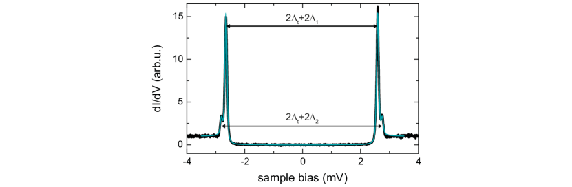
A clean -NbSe2 surface is prepared by cleaving a bulk crystal (grown by iodine vapor transport Rahn et al. (2012)) in ultra-high vacuum. Scanning tunneling spectroscopy (performed by standard lock-in techniques at a temperature of K) shows that the superconducting energy gap of the substrate is framed by characteristic coherence peaks in an energy range of (black spectrum in Fig. 1e). The origin of this peculiar quasiparticle density of states (DOS) has been discussed in terms of multiband or anisotropic superconductivity Hess et al. (1990); Yokoya et al. (2001); Noat et al. (2010, 2015); Rodrigo and Vieira (2004); Boaknin et al. (2003); Fletcher et al. (2007); Guillamón et al. (2008a, b). Notice that we use superconducting Pb tips to improve the energy resolution beyond the Fermi-Dirac limit. The convolution of the DOS of tip and substrate shifts all spectral features by the tip’s energy gap (for details see Supporting Information (SI) SM ).
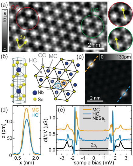
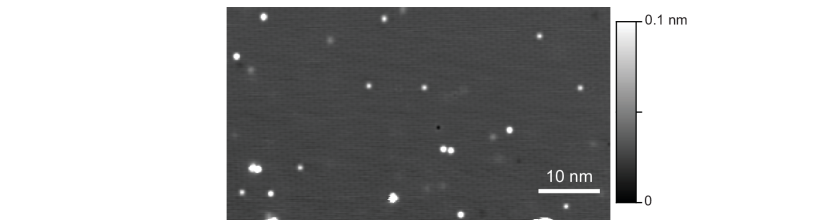
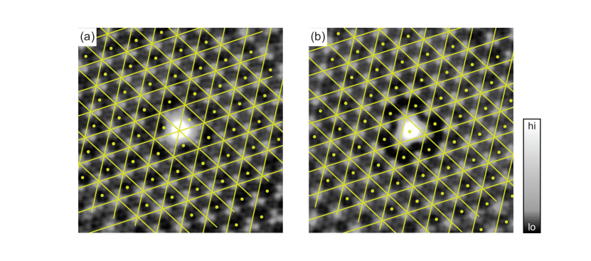
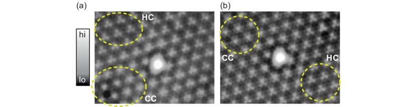
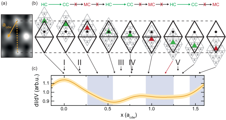
Scanning tunneling microscopy (STM) images of the clean surface clearly reveal the modulation of the local DOS induced by the CDW superimposed on the atomic corrugation (Fig. 1a). The CDW has a lattice constant , making it incommensurate with the underlying atomic lattice. Thus, the phase of the CDW relative to the atomic lattice varies smoothly across the surface Gye et al. (2019); Guster et al. (2019). The close-ups show two extremal cases for which the maxima coincide either with a Se atom (chalcogen-centered, CC, red circle in Fig. 1a and Fig. 1b) or a hollow site (hollow-centered, HC, green circle in Fig. 1a and Fig. 1b SC (1)).
Fe atoms (deposited at temperatures below 12 K into the STM) appear as two stable species with different apparent heights (Fig. 1c,d). By atomic-resolution imaging (for details see SI SM ), we assign adatoms with small and large apparent height to adsorption in the two inequivalent hollow sites of the terminating Se layer, identified as hollow-centered (HC) and metal-centered (MC) sites, respectively (Fig. 1b) SC (3). spectra taken above the centers of HC and MC adatoms (blue and orange in Fig. 1e) show several YSR states inside the superconducting gap as well as in the energy range of the substrate’s coherence peaks as has been observed previously for buried impurities Senkpiel et al. (2019). The energy and intensity of the YSR states differ between the two species. Presumably, the splitting of the adatom -levels is sensitive to the different local environments of the adsorption sites, which in turn affects the potential- and exchange-scattering strengths Ruby et al. (2016).
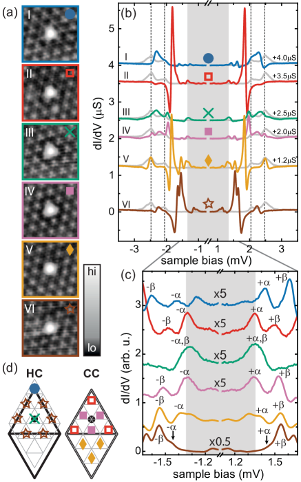
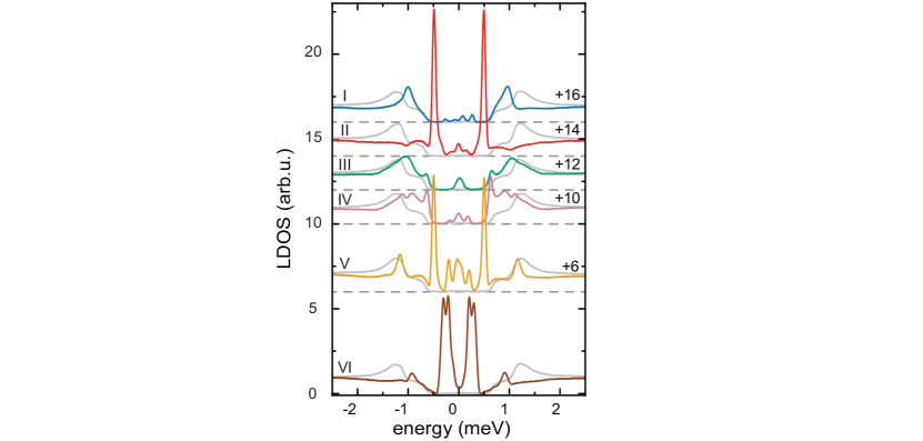
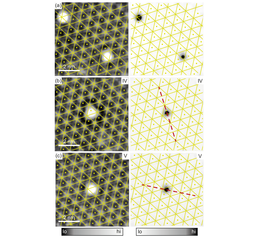
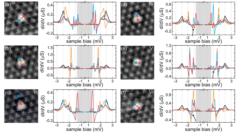
To isolate the influence of the CDW, we focus on Fe atoms which are all sitting in the same atomic adsorption site (HC) in the following. Six different atoms (labeled by I-VI) are shown in Fig. 2a. The corresponding spectra (Fig. 2b) reveal that the energy and intensity of their YSR states differ strongly even though their atomic adsorption sites are identical with respect to the unperturbed lattice.
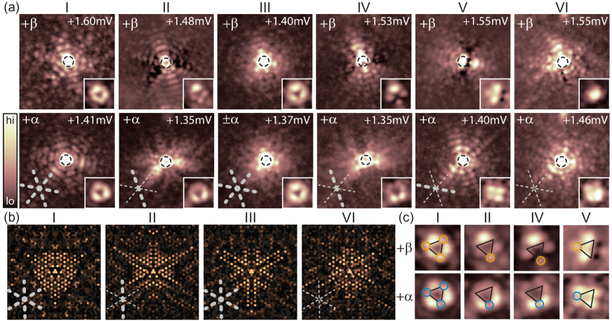
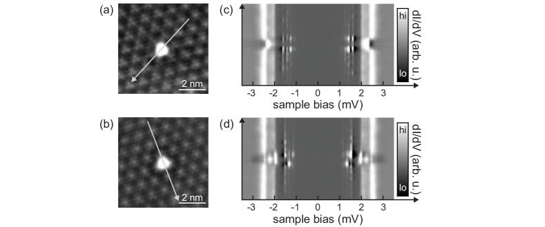
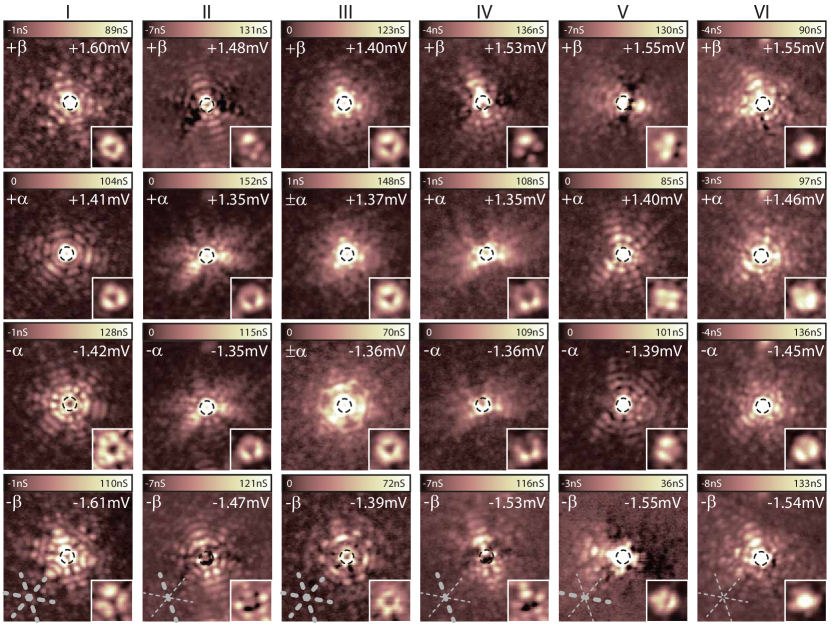
YSR states in the energy range of the superconducting coherence peaks are difficult to disentangle from the background. To avoid this complication, we focus on deep-lying YSR states, specifically the two lowest YSR pairs labeled as and in the close-up view presented in Fig. 2c. maps recorded at the corresponding bias voltages and are shown in Fig. 3a for adatoms I-VI. The main panels show the extended patterns while the insets focus on the immediate vicinity of the adatom. All extended maps show patterns with oscillating intensity SC (2). The overall symmetries of the patterns clearly differ between adatoms I-VI.
The symmetry of the patterns associated with YSR states is expected to originate from the anisotropy of the Fermi surface Salkola et al. (1997); Flatté and Byers (1997) and the local crystal field Ruby et al. (2016). The threefold-symmetric atomic adsorption site together with the sixfold symmetry of the Fermi surface should therefore lead to symmetry (threefold rotation as well as three mirror axes, cf. dashed lines in Fig. 1b). Interestingly, this symmetry is observed for both YSR states and of adatoms I and III, which reside at a maximum and a minimum of the CDW, respectively (Figs. 2d, 3a). However, this symmetry is lost in both, the long-range and the immediate vicinity of the adatoms for the other atoms shown in Fig. 3a. For adatoms II, IV, and V, the symmetry is reduced to symmetry (single mirror axis) while no symmetry axis can be discerned for adatom VI.
The symmetry reductions of the YSR patterns coincide with the reductions of the local symmetry of the adsorption sites by the CDW (Fig. 2d). Adatoms I and III are positioned at a maximum or a minimum of the CDW, so that the CDW respects the atomic symmetry (HC structure of the CDW). Atoms II, IV, and V are located on one of the three equivalent symmetry axes connecting the high-symmetry positions, but unlike adatoms I and III do not directly fall on an extremum (CDW in the CC domain). Thus, the CDW breaks the atomic symmetry, leaving only symmetry consistent with the observed YSR patterns. Finally, the position of adatom VI is totally asymmetric with respect to the CDW, which is reflected in the absence of any symmetry in the corresponding maps.
The microscopic physics behind these symmetry reductions can be understood theoretically within a phenomenological mean-field description of the CDW combined with a tight-binding model of the -NbSe2 band structure. Foregoing a realistic description of the Fe -orbital physics, we model the adatom as a classical impurity with isotropic potential and exchange couplings to the substrate (see SI SM for details). Due to the electron-phonon interaction, the CDW acts on the electrons as a weakly incommensurate, static periodic potential. This potential reduces the symmetry of the YSR wavefunctions in a manner consistent with the experimental results. Corresponding numerical results are shown in Fig. 3b for a subset of the adsorption sites investigated experimentally (see SI SM for the remaining sites and further details). We find that the wavefunctions (and the number) of the YSR states are quite sensitive to details of the band structure and the neglected -orbital physics, so that one expects agreement only for qualitative aspects of symmetry.
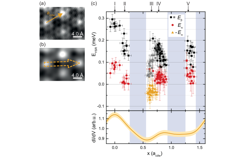
So far, the assignments and for the YSR states simply refer to the two deepest resonances. Analyzing the observed YSR patterns allows us to track these two YSR states as a function of position relative to the CDW. For the YSR state of adatom I, the short-range pattern exhibits a triangular shape (Fig. 3c) with high intensity on its sides and slightly smaller intensity at its vertices (orange circles). In contrast, the YSR state for adatom I lacks intensity at the vertices (blue circles) and thus exhibits pronounced nodes. Signatures of this distinction persist at the lower-symmetry positions II, IV, and V. While the intensity distributions change for both states, we still observe distinct intensities at one of the vertices which distinguish between the and resonances (while present, the distinction is somewhat less pronounced for adatom V, see also SI SM ). A similar distinction cannot be made for adatom III. We attribute this to the fact that in this case, both the - and the -resonances lie very close to the Fermi level. This prevents us from individually resolving them within our energy resolution (Fig. 2c, green trace).
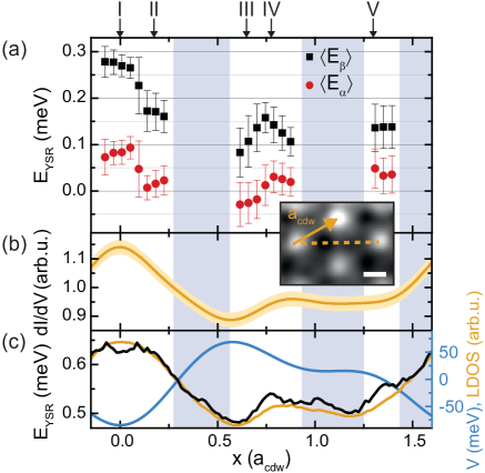
With these characteristics, we can track the resonances as a function of position relative to the CDW and probe its effect on the YSR energies. As the CDW transforms smoothly between HC and CC domains, we can study numerous positions along its symmetry axis (such as positions II, IV, and V in Fig. 2d, but also in between). Altogether, we analyze approximately adatoms adsorbed close to one of the three equivalent CDW symmetry axes, combining data from several samples and Pb tips. For all adatoms, we extract the energies of the YSR states by deconvolving the spectra to remove the influence of the Pb tip (see SI SM ). Figure 4a plots the energies of both the and states as a function of adatom position along a high-symmetry axis of the CDW. Here, we assume that the energy dependences of both resonances follow the same trend which implies that the energy of the resonance changes sign and crosses the quantum phase transition from a screened-spin to a free-spin ground state Choi et al. (2017); Franke et al. (2011); Farinacci et al. (2018); Malavolti et al. (2018) as a function of adatom position. Note that some regions (shaded in Fig. 4a) of adatom positions remain inaccessible for Fe atoms in HC sites, because the CDW maxima avoid MC domains SC (1).
A qualitatively similar dependence of the energy of the YSR states is found in our model calculations (Fig. 4c and SI SM ). The YSR energies are (anti)correlated with the CDW potential and the local DOS, with the type of correlation depending on whether the impurity is in the weak- or strong-coupling regime and on the strength of potential scattering by the impurity SM . (We find that the CDW potential is anticorrelated with the local DOS.) Except for very strong potential scattering (see SI SM ), our results are consistent with a simple model for the energy of YSR states Yu (1965); Shiba (1968); Rusinov (1969),
| (1) |
Here, is the superconducting gap, the (classical) spin, the exchange coupling, and the local DOS of the superconductor. This predicts that YSR energies are (anti)correlated with the local DOS for impurities in the strong (weak) coupling limit. Experimentally, we record a constant-height map at zero bias above and remove the atomic corrugation by an FFT filter (cf. inset Fig. 4b). The remaining signal is proportional to the local DOS due to the CDW at the Fermi level. We find that the YSR energies correlate with the local DOS as seen in Fig. 4a,b. This suggests that the YSR states are in most of the adsorption sites in the strong-coupling regime. Only when the Fe atoms are located in the minima of the CDW, resonance undergoes the quantum phase transition to the free-spin ground state.
In conclusion, we find that the properties of YSR states are strongly affected by CDW ordering. The CDW shifts the energy of YSR states and reduces the symmetry of YSR wavefunctions both in the immediate vicinity of and further from the adatoms. These observations impose stringent constraints on the design of strongly coupled magnetic adatom structures on NbSe2 substrates. Neverthless, NbSe2 remains a highly attractive substrate in this context, owing to the long-range nature of the YSR states and its suitability for adatom manipulation. Our results extend to truly two-dimensional NbSe2 substrates with their promise of device applications. Indeed, single-layer NbSe2 also exhibits an incommensurate CDW Guster et al. (2019); Ugeda et al. (2016). Importantly, pairing correlations in single-layer NbSe2 are remarkably robust against in-plane fields as a consequence of spin-valley locking (Ising superconductivity) Xi et al. (2016). This may enable measurements of YSR states at magnetic fields which polarize the adatom spin without suppressing superconductivity. The interaction of YSR states with superconductivity, charge-density order, and external magnetic fields entails substantial flexibility to tune into or control a topologically non-trivial superconducting phase. Finally, our study suggests that YSR states provide a sensitive probe of these competing interactions which should extend to other systems.
Acknowledgements.
Financial support by Deutsche Forschungsgemeinschaft through grant CRC 183 (FvO), as well as by the European Research Council through the consolidator grant “NanoSpin” (KJF) is gratefully acknowledged.References
- Hess et al. (1990) H. F. Hess, R. B. Robinson, and J. V. Waszczak, Phys. Rev. Lett. 64, 2711 (1990).
- Yokoya et al. (2001) T. Yokoya, T. Kiss, A. Chainani, S. Shin, M. Nohara, and H. Takagi, Science 294, 2518 (2001).
- Noat et al. (2010) Y. Noat, T. Cren, F. Debontridder, D. Roditchev, W. Sacks, P. Toulemonde, and A. San Miguel, Phys. Rev. B 82, 014531 (2010).
- Noat et al. (2015) Y. Noat, J. A. Silva-Guillén, T. Cren, V. Cherkez, C. Brun, S. Pons, F. Debontridder, D. Roditchev, W. Sacks, L. Cario, P. Ordejón, A. García, and E. Canadell, Phys. Rev. B 92, 134510 (2015).
- Rodrigo and Vieira (2004) J. G. Rodrigo and S. Vieira, Physica C 404, 306 (2004).
- Boaknin et al. (2003) E. Boaknin, M. A. Tanatar, J. Paglione, D. Hawthorn, F. Ronning, R. W. Hill, M. Sutherland, L. Taillefer, J. Sonier, S. M. Hayden, and J. W. Brill, Phys. Rev. Lett. 90, 117003 (2003).
- Fletcher et al. (2007) J. D. Fletcher, A. Carrington, P. Diener, P. Rodière, J. P. Brison, R. Prozorov, T. Olheiser, and R. W. Giannetta, Phys. Rev. Lett. 98, 057003 (2007).
- Guillamón et al. (2008a) I. Guillamón, H. Suderow, F. Guinea, and S. Vieira, Phys. Rev. B 77, 134505 (2008a).
- Guillamón et al. (2008b) I. Guillamón, H. Suderow, S. Vieira, L. Cario, P. Diener, and P. Rodière, Phys. Rev. Lett. 101, 166407 (2008b).
- Xi et al. (2016) X. Xi, Z. Wang, W. Zhao, J.-H. Park, K. T. Law, H. Berger, L. Forró, J. Shan, and K. F. Mak, Nature Phys. 12, 139 (2016).
- Ugeda et al. (2016) M. M. Ugeda, A. J. Bradley, Y. Zhang, S. Onishi, Y. Chen, W. Ruan, C. Ojeda-Aristizabal, H. Ryu, M. T. Edmonds, H.-Z. Tsai, and et al., Nature Phys. 12, 92 (2016).
- Rossnagel et al. (2001) K. Rossnagel, O. Seifarth, L. Kipp, M. Skibowski, D. Voß, P. Krüger, A. Mazur, and J. Pollmann, Phys. Rev. B 64, 235119 (2001).
- Johannes et al. (2006) M. D. Johannes, I. I. Mazin, and C. A. Howells, Phys. Rev. B 73, 205102 (2006).
- Kiss et al. (2007) T. Kiss, T. Yokoya, A. Chainani, S. Shin, T. Hanaguri, M. Nohara, and H. Takagi, Nature Phys. 3, 720 (2007).
- Johannes and Mazin (2008) M. D. Johannes and I. I. Mazin, Phys. Rev. B 77, 165135 (2008).
- Rahn et al. (2012) D. J. Rahn, S. Hellmann, M. Kalläne, C. Sohrt, T. K. Kim, L. Kipp, and K. Rossnagel, Phys. Rev. B 85, 224532 (2012).
- Malliakas and Kanatzidis (2013) C. D. Malliakas and M. G. Kanatzidis, J. Am. Chem. Soc. 135, 1719 (2013).
- Dai et al. (2014) J. Dai, E. Calleja, J. Alldredge, X. Zhu, L. Li, W. Lu, Y. Sun, T. Wolf, H. Berger, and K. McElroy, Phys. Rev. B 89, 165140 (2014).
- Arguello et al. (2014) C. J. Arguello, S. P. Chockalingam, E. P. Rosenthal, L. Zhao, C. Gutiérrez, J. H. Kang, W. C. Chung, R. M. Fernandes, S. Jia, A. J. Millis, R. J. Cava, and A. N. Pasupathy, Phys. Rev. B 89, 235115 (2014).
- Arguello et al. (2015) C. J. Arguello, E. P. Rosenthal, E. F. Andrade, W. Jin, P. C. Yeh, N. Zaki, S. Jia, R. J. Cava, R. M. Fernandes, A. J. Millis, T. Valla, R. M. Osgood, and A. N. Pasupathy, Phys. Rev. Lett. 114, 037001 (2015).
- Flicker and van Wezel (2015) F. Flicker and J. van Wezel, Nature Commun. 6, 7034 (2015).
- Soumyanarayanan et al. (2013) A. Soumyanarayanan, M. M. Yee, Y. He, J. van Wezel, D. J. Rahn, K. Rossnagel, E. W. Hudson, M. R. Norman, and J. E. Hoffman, Proc. Natl. Acad. Sci. 110, 1623 (2013).
- Weber et al. (2011) F. Weber, S. Rosenkranz, J.-P. Castellan, R. Osborn, R. Hott, R. Heid, K.-P. Bohnen, T. Egami, A. H. Said, and D. Reznik, Phys. Rev. Lett. 107, 107403 (2011).
- Suderow et al. (2005) H. Suderow, V. G. Tissen, J. P. Brison, J. L. Martínez, and S. Vieira, Phys. Rev. Lett. 95, 117006 (2005).
- Borisenko et al. (2009) S. V. Borisenko, A. A. Kordyuk, V. B. Zabolotnyy, D. S. Inosov, D. Evtushinsky, B. Büchner, A. N. Yaresko, A. Varykhalov, R. Follath, W. Eberhardt, L. Patthey, and H. Berger, Phys. Rev. Lett. 102, 166402 (2009).
- Cho et al. (2018) K. Cho, M. Kończykowski, S. Teknowijoyo, M. A. Tanatar, J. Guss, P. Gartin, J. M. Wilde, A. Kreyssig, R. McQueeney, A. I. Goldman, et al., Nature Commun. 9, 2796 (2018).
- Sticlet and Morari (2019) D. Sticlet and C. Morari, Phys. Rev. B 100, 075420 (2019).
- Głodzik and Ojanen (2019) S. Głodzik and T. Ojanen, arXiv , 1905.01063 (2019), arXiv:arXiv:1905.01063 .
- Nadj-Perge et al. (2014) S. Nadj-Perge, I. K. Drozdov, J. Li, H. Chen, S. Jeon, J. Seo, A. H. MacDonald, B. A. Bernevig, and A. Yazdani, Science 346, 602 (2014).
- Nadj-Perge et al. (2013) S. Nadj-Perge, I. K. Drozdov, B. A. Bernevig, and A. Yazdani, Phys. Rev. B 88, 020407 (2013).
- Pientka et al. (2013) F. Pientka, L. I. Glazman, and F. von Oppen, Phys. Rev. B 88, 155420 (2013).
- Yu (1965) L. Yu, Acta Phys. Sin. 21, 75 (1965).
- Shiba (1968) H. Shiba, Prog. Theor. Phys. 40, 435 (1968).
- Rusinov (1969) A. I. Rusinov, JETP Lett. 9, 85 (1969).
- Yazdani et al. (1997) A. Yazdani, B. A. Jones, C. P. Lutz, M. F. Crommie, and D. M. Eigler, Science 275, 1767 (1997).
- Ménard et al. (2015) G. C. Ménard, S. Guissart, C. Brun, S. Pons, V. S. Stolyarov, F. Debontridder, M. V. Leclerc, E. Janod, L. Cario, D. Roditchev, P. Simon, and T. Cren, Nature Phys. 11, 1013 (2015).
- Kezilebieke et al. (2018) S. Kezilebieke, M. Dvorak, T. Ojanen, and P. Liljeroth, Nano Lett. 18, 2311 (2018).
- Ruby et al. (2018) M. Ruby, B. W. Heinrich, Y. Peng, F. von Oppen, and K. J. Franke, Phys. Rev. Lett. 120, 156803 (2018).
- Choi et al. (2018) D.-J. Choi, C. G. Fernández, E. Herrera, C. Rubio-Verdú, M. M. Ugeda, I. Guillamón, H. Suderow, J. I. Pascual, and N. Lorente, Phys. Rev. Lett. 120, 167001 (2018).
- Kamlapure et al. (2018) A. Kamlapure, L. Cornils, J. Wiebe, and R. Wiesendanger, Nature Commun. 9, 1 (2018).
- Kim et al. (2018) H. Kim, A. Palacio-Morales, T. Posske, L. Rózsa, K. Palotás, L. Szunyogh, M. Thorwart, and R. Wiesendanger, Science Advances 4, eaar5251 (2018) .
- Senkpiel et al. (2019) J. Senkpiel, C. Rubio-Verdú, M. Etzkorn, R. Drost, L. M. Schoop, S. Dambach, C. Padurariu, B. Kubala, J. Ankerhold, C. R. Ast, and K. Kern, Phys. Rev. B 100, 014502 (2019).
- Ji et al. (2008) S.-H. Ji, T. Zhang, Y.-S. Fu, X. Chen, X.-C. Ma, J. Li, W.-H. Duan, J.-F. Jia, and Q.-K. Xue, Phys. Rev. Lett. 100, 226801 (2008).
- Ruby et al. (2015) M. Ruby, F. Pientka, Y. Peng, F. von Oppen, B. W. Heinrich, and K. J. Franke, Phys. Rev. Lett. 115, 087001 (2015).
- Ruby et al. (2016) M. Ruby, Y. Peng, F. von Oppen, B. W. Heinrich, and K. J. Franke, Phys. Rev. Lett. 117, 186801 (2016).
- Choi et al. (2017) D.-J. Choi, C. Rubio-Verdú, J. De Bruijckere, M. M. Ugeda, N. Lorente, and J. I. Pascual, Nature Commun. 8, 15175 (2017).
- Cornils et al. (2017) L. Cornils, A. Kamlapure, L. Zhou, S. Pradhan, A. A. Khajetoorians, J. Fransson, J. Wiebe, and R. Wiesendanger, Phys. Rev. Lett. 119, 197002 (2017).
- (48) Supporting Information.
- Gye et al. (2019) G. Gye, E. Oh, and H. W. Yeom, Phys. Rev. Lett. 122, 016403 (2019).
- Guster et al. (2019) B. Guster, C. Rubio-Verdú, R. Robles, J. Zaldívar, P. Dreher, M. Pruneda, J. Á. Silva-Guillén, D.-J. Choi, J. I. Pascual, M. M. Ugeda, P. Ordejón, and E. Canadell, Nano Lett. 19, 3027 (2019).
- SC (1) Areas with Nb-centered CDW maxima (metal-centered, MC) do not appear in the STM images, as they have higher energy Gye et al. (2019); Guster et al. (2019). See SI SM , especially Fig. S18 for further details.
- SC (3) In addition to the apparent height, both species also differ in the energies of their -level resonances. We note that the apparent heights and -level resonances are only slightly affected by the CDW. See SI SM for more details.
- SC (2) The long-range oscillations are expected to have a period of half the Fermi wavelength in simple models of YSR states Rusinov (1969). The Fermi surface of -NbSe2 consists of several sheets Yokoya et al. (2001); Kiss et al. (2007); Rahn et al. (2012); Rossnagel et al. (2001) which can lead to a more complex structure in the long-range scattering pattern of the YSR wavefunctions.
- Salkola et al. (1997) M. I. Salkola, A. V. Balatsky, and J. R. Schrieffer, Phys. Rev. B 55, 12648 (1997).
- Flatté and Byers (1997) M. E. Flatté and J. M. Byers, Phys. Rev. Lett. 78, 3761 (1997).
- Franke et al. (2011) K. J. Franke, G. Schulze, and J. I. Pascual, Science 332, 940 (2011).
- Farinacci et al. (2018) L. Farinacci, G. Ahmadi, G. Reecht, M. Ruby, N. Bogdanoff, O. Peters, B. W. Heinrich, F. von Oppen, and K. J. Franke, Phys. Rev. Lett. 121, 196803 (2018).
- Malavolti et al. (2018) L. Malavolti, M. Briganti, M. Hänze, G. Serrano, I. Cimatti, G. McMurtrie, E. Otero, P. Ohresser, F. Totti, M. Mannini, R. Sessoli, and S. Loth, Nano Lett. 18, 7955 (2018).
- Note (1) Note that the experimental adsorption site falls in the middle of a Nb triangle. Such an impurity has equal couplings to the three neighboring Nb atoms. When modeling the impurity as a classical impurity, this easily leads to spurious YSR states which would not be present for a quantum impurity. In view of the fact that our treatment of the impurity is highly simplified in any case, we avoid this problem by placing the impurity on a Nb site.
Supporting Information
S1 Theoretical considerations
S1.1 Mean-field description of the charge-density wave
We resort to a phenomenological mean-field description. We start with a generic Fröhlich-type Hamiltonian describing electrons coupled to phonons Grüner (1994),
| (S1) |
Here, annihilates electrons with momentum and energy , annihilates a phonon with wavevector and frequency , and denotes the strength of the electron-phonon coupling. Within mean-field theory, we assume that certain phonon modes (denoted by ) go soft due to their coupling to the electronic system and develop a finite expectation value. Restricting to the lowest Fourier components and neglecting phonon dynamics beyond the static charge-density wave (CDW) distortions, we find the mean-field Hamiltonian
| (S2) |
for the electronic degrees of freedom. Within this approach, the CDW acts on the electrons as a periodic potential . Indeed, the electron-phonon interaction term can also be expressed in real space as
| (S3) |
where the mean-field CDW potential takes the form
| (S4) |
To find the vectors Q, we consider a triangular lattice of Nb atoms with lattice vectors
| (S5) | ||||
| (S6) |
and bond length Å. The corresponding reciprocal lattice vectors satisfying are
| (S7) | ||||
| (S8) |
The unit cell of the CDW has a linear dimension which is approximately three times larger than the unit cell of the atomic lattice, (for ). Correspondingly, the reciprocal lattice vectors of the CDW are approximately a factor of three smaller, . Then, the first harmonics of the CDW have wavevectors
| (S9) | ||||
where , and accounts for the fact that the CDW is not exactly commensurate with the lattice.
S1.2 Tight-binding model
To illustrate the effect of the CDW on the YSR state wavefunction, we perform model calculations within an effective tight-binding description. Specifically, we implement a model for the NbSe2 band structure first introduced in Ref. Smith et al. (1985) and later used in Refs. Rossnagel et al. (2005); Inosov et al. (2008, 2009); Rahn et al. (2012); Ménard et al. (2015). The model uses that the relevant states near the Fermi energy have mostly Nb character and therefore focuses on one atomic -orbital per niobium atom. (The model neglects an additional band centered at the point which predominantly derives from Se orbitals and has strongly three-dimensional character Bawden et al. (2016).) Reducing the band-structure problem to the triangular Nb lattice makes it necessary to include hopping up to fifth nearest neighbors to reproduce the NbSe2 band structure. The resulting band structure
| (S10) |
| band 1 | 10.9 | 86.8 | 139.9 | 29.6 | 3.5 | 3.3 |
| band 2 | 203.0 | 46.0 | 257.5 | 4.4 | -15.0 | 6.0 |
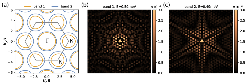
is sixfold symmetric about the point. Here, we defined and . The hopping strengths are used as fitting parameters to reproduce the NbSe2 band structure. The values of the parameters are given in Table S1 Rahn et al. (2012) for the two bands. The parameters for band 1 reproduce the inner cylindrical bands of NbSe2, while the parameters for band 2 reproduce the outer bands. Figure S1a shows the Fermi surfaces of the two bands, with the Brillouin zone outlined in gray.
While this model accounts for the symmetries of the band structure and the approximate shapes of the Fermi surfaces, it is limited in other ways. The model neglects interlayer coupling which, however, is expected to be weak compared to the intralayer couplings. In this approximation, it suffices to consider a single (tri)layer of -NbSe2, consisting of a Nb layer sandwiched between two Se layers with equal orientations of the triangles. The model also neglects spin-orbit coupling Xi et al. (2016). This precludes a one-to-one identification of the two sets of bands in Fig. S1a with specific spin directions.
The elementary layer of bulk -NbSe2 consists of two trilayers with the orientations of the Se lattices rotated by with respect to one another. Neglecting interlayer coupling, the band structure of the second trilayer is identical to the first (but differs in the spin assignments). Thus, the bulk crystal has twofold degenerate bands, consistent with the fact that it has an inversion center located between the trilayers. The adatom predominantly couples to one of the trilayers and the band structure in Eq. (S10) should be a good starting point. In the following, we follow Ref. Ménard et al. (2015) in neglecting the splitting between the two sets of bands and model the system either by band 1 or band 2, taking these bands as spin degenerate.
Superconductivity is included by incorporating the tight-binding Hamiltonian into a Bogoliubov-deGennes Hamiltonian with conventional (isotropic) -wave pairing. We choose the pairing strength to be meV. In experiment, one finds multiple coherence peaks for -NbSe2. Since we focus on YSR states far from the gap edge, we choose a representative value for which falls into the range of the peak distribution ( meV) found in experiment.
The multiple coherence peaks originate from multiband or anisotropic superconductivity, or both. Our modeling does not account for these effects. In principle, an anisotropic gap function affects the wavefunction patterns of the YSR states. However, the (observable) spatial extent of YSR states is smaller than the coherence length through which effects of the pairing function would enter. We thus expect that the effect of an anisotropic pairing function on the YSR wavefunctions is weak and therefore account for superconductivity via an isotropic pairing function.
S1.3 Coupling to the magnetic impurity
While the origin of the magnetic moment and the resulting exchange coupling can be understood starting with an Anderson model and its mapping to a Kondo Hamiltonian in the absence of valence fluctuations (see Ref. Hewson (1993) for an extensive pedagogical discussion), YSR states are typically well described within a model which treats the impurity spin in the Kondo model as classical Yu (1965); Shiba (1968a); Rusinov (1969). For YSR states in NbSe2, this model was previously used in Ref. Ménard et al. (2015). Following this reference, we model a magnetic impurity as a classical spin which interacts with the substrate electrons through the exchange interaction and accompanying potential scattering . In our experiment, we focus on magnetic impurities located above the center of a Nb triangle (hollow-centered, see Fig. 1b of the main text). The impurity induces not only separate exchange and potential couplings to its three neighbors, but also nonlocal exchange couplings which scatter electrons between the three sites via the impurity. It is essential to retain the latter to ensure that the impurity induces only one pair of YSR resonances. If we assume identical hopping amplitudes between the three sites and the impurity and assume that the impurity spin is aligned along the -direction, we obtain the exchange coupling
| (S11) |
and potential scattering terms
| (S12) |
Here, the sums over and run over the three nearest-neighbor Nb sites of the impurity, denotes a Pauli matrix, and annihilates an electron on site with spin .
Figures S1b and c show the probability densities of the YSR states for (a spin-degenerate version of) bands 1 and 2, respectively, for a specific choice of impurity parameters. The spatial distribution of the probability density is threefold symmetric in both cases. Due to the more isotropic character of band 1, the corresponding YSR state is also more spatially isotropic than its band 2 counterpart, which exhibits a more pronounced anisotropy. In a more realistic modeling including the effects of spin-orbit coupling on the band structure (but within the approximation that the impurity is coupled only to a single trilayer), the YSR states would be simultaneously coupled to spin-textured, but polarized versions of both bands. While this implies that our results for the YSR wavefunctions are only qualitative, the symmetry of the YSR wavefunctions should not be affected by this approximation. Similarly, we expect that the qualitative variation of the YSR energies with the location of the adsorption site relative to the CDW would also be unaffected.
We note that in our approximation, there is only a single pair of YSR states for a classical magnetic impurity. In fact, this conclusion would remain valid even when spin-orbit splitting of the bands was taken into account. On the one hand, it is known that even in multiband situations, a classical magnetic impurity induces only a single pair of YSR states. In fact, if we write the matrix of exchange couplings between bands and , it rather robustly satisfies the relation . With this relation, a classical magnetic impurity generates only a single pair of YSR states. For instance, this was shown explicitly for a generic model motivated by the multiband superconductor MgB2 Moca et al. (2008) and for a quantum dot coupled to multiple superconducting leads Kirs̆anskas et al. (2015). In the presence of spin-orbit coupling, the same conclusions can be shown to remain valid. This can be seen by expressing the Hamiltonian in terms of creation and annihilation operators for Kramers pairs of electron states rather than conventional spin states.
S1.4 Coupling to the charge-density wave
As explained above, the effect of the CDW on the electrons of the substrate can be described through a periodic potential. Within the tight-binding model, we include the CDW as a modulation of the on-site potential,
| (S13) |
where the sum runs over the lattice sites of the triangular Nb lattice. The CDW potential is constructed from the main Fourier components of the CDW see Eq. (S9),
| (S14) |
where denotes the amplitude of the CDW potential. Except for and similar fine-tuned cases, typical choices of the phases yield CDW potentials with the desired symmetry and shape, exhibiting an absolute maximum, an absolute minimum, and a local minimum/saddle point. For definiteness, we choose .
Due to the small deviations from commensurability, the CDW shifts slowly as a function of position relative to the underlying atomic lattice. On the scale of the YSR states, these shifts can be considered constant so that the CDW potential can be written as
| (S15) |
where . The offsets and originate from the deviation from commensurability, and describe the local shift of the CDW relative to the atomic lattice. In the experiment, the measured maxima of the CDW correspond to regions where the lattice deformation compresses the ions, creating an attractive potential for the electrons. For this reason we choose the potential to have minima where the measured tunneling density of states has maxima, i.e., position I of the adatom corresponds to a minimum of and position III corresponds to a maximum. In principle, the CDW may also modulate the hopping parameters of the tight-binding model, but the effective long-range hopping processes of the model make this cumbersome to include.
We note that this model also includes configurations of the CDW relative to the atomic lattice which are not observed experimentally (see Fig. S18). Theoretical results for these unobserved configurations are only included for completeness. The results for observed configurations are not affected since the Moire-like variations occur on relatively large scales.
S1.5 Numerical results
Within this model, we can study how the wavefunction and the energy of YSR states depend on the adatom position relative to the CDW. As discussed above, the model cannot reproduce the experimental results quantitatively as it neglects various relevant effects. Nevertheless, the model is expected to capture the symmetries of the YSR wavefunctions and to provide insights into the qualitative dependence of the YSR energy on the adsorption site relative to the CDW.
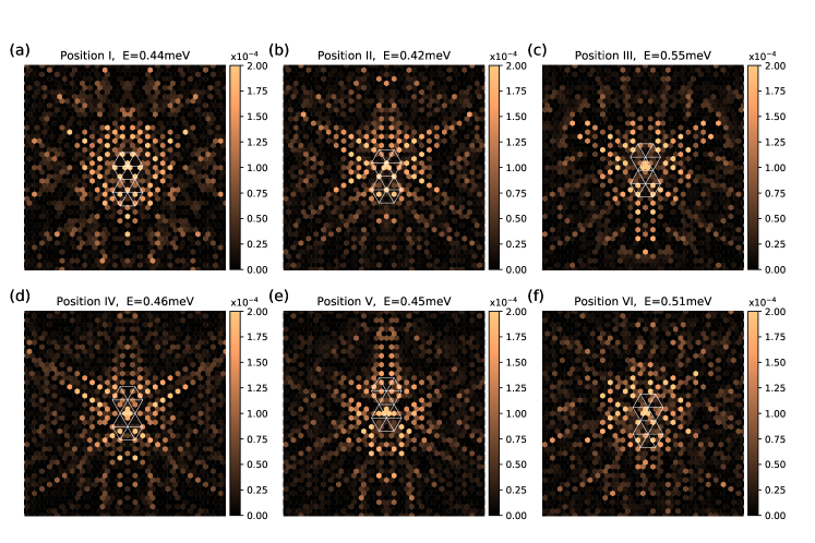
Figure S2 shows the probability density of the YSR wavefunction for the six different positions of the adatom relative to the CDW, as discussed in the main text. The results are obtained for the parameters of band 2. The adatoms in positions I and III are at the maximum and the minimum of the CDW, respectively, i.e., at points with a threefold symmetric environment. Consequently, the corresponding density plots (Fig. S2a and c) present threefold symmetry. Positions II, IV, and V exhibit reflection symmetry about an axis that passes through the adatom. For the corresponding plots shown in Fig. S2b, d, and e, this axis is aligned along the vertical direction. Finally, position VI has no symmetries with respect to the CDW and consequently, the state shown in Fig. S2f also exhibits no symmetries. Interestingly, the YSR state seems to retain the original threefold symmetry (without CDW) to some degree (compare with Fig. S1c).
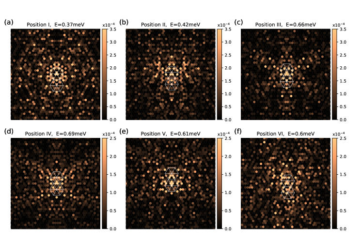
Figure S3 shows equivalent plots for band 1. Due to the more isotropic character of band 1, the threefold symmetry is less pronounced in these plots. Remarkably, position VI (Fig. S3f) does not preserve any of the original threefold symmetry in the vicinity of the adatom. More generally, a comparison between Figs. S2 and S3 shows that the detailed YSR wavefunctions depend quite sensitively on the band structure parameters.
Finally, we discuss the correlation of the energy of the YSR state with the modulation of the local density of states by the CDW, as shown in Fig. 4 in the main text. Within a simple model of a classical magnetic impurity, the energy of YSR states depends on the strength of the exchange coupling as measured by the dimensionless parameter , where is the density of states, the exchange coupling, and the impurity spin. Thus, one indeed expects the energy of the YSR state to depend on the density of states . The direction of the energy shift depends on whether the impurity is weakly or strongly coupled, corresponding to unscreened or (partially) screened impurity spins, respectively. The energy of the positive-energy YSR state decreases (increases) with the density of states, depending on whether the impurity spin is unscreened (screened). Variations in the local density of states due to the CDW should thus be reflected in the energy of the YSR states. Within this picture, the observed correlations suggest that in our experiment the impurity is in the strong-coupling limit.
This interpretation is consistent with our theoretical results. However, we find that in general the CDW affects the energy of the YSR state through two mechanisms. In addition to the density of states effect, the CDW potential has a second effect which can be roughly rationalized as the CDW affecting the strength of potential scattering from the impurity and thereby shifting the YSR energy. Including potential scattering within the simple model, the energy of a YSR state is given by Yu (1965); Shiba (1968b); Rusinov (1969)
| (S16) |
where is a dimensionless measure of the strength of the potential scattering . The transition between weak and strong coupling takes place at where the energy of the YSR state passes through zero. Roughly, the CDW potential seems to shift to , where denotes the adsorption site of the impurity. For comparison with experiment, it is important to note that an increase in the CDW potential decreases the density of states. This can be seen in e.g. Fig. S4g, which shows numerical results for the average local density of states of the three sites coupled to the impurity (orange) in the presence of the CDW potential (blue) as obtained from a straight-forward band structure calculation. Thus, the experiment implies an anticorrelation between the CDW potential and the energy of the YSR states.
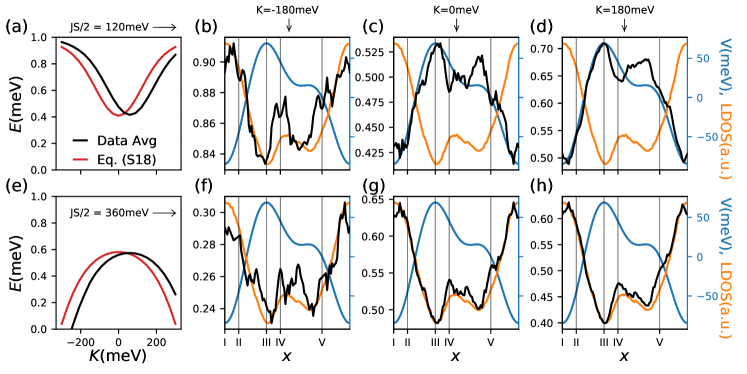
To illustrate these two effects of the CDW potential, we calculate the YRS energy for different adatom positions and various values of . Consider first the results for weak coupling. We find that depending on the strength of potential scattering, the CDW potential is correlated or anticorrelated with the energy of the YSR state. For meV and , the energy is correlated with the CDW potential, see Fig. S4c and d. In contrast, we find anticorrelations for meV, see Fig. S4b. The correlations observed at are consistent with the effect of the CDW potential on the density of states. At this , the energy shift of the YSR state due to the change in potential scattering, to , is weak since the energy of the YSR states is only weakly dependent on near the minimum at . This is illustrated in Fig. S4a which shows the dependence of the energy of the YSR state on in the weak-coupling regime. Specifically, the black curve averages data for the energy of the YSR state over different adatom positions. The red curve corresponds to Eq. (S16) with the same values for and and an appropriately chosen density of states . Both curves exhibit similar ‘parabolic’ behaviors.
For the strongly coupled regime, we find anticorrelations between the CDW potential and the energy of the YSR state – and thus correlations between the local density of states and the YSR energy – for all values of , see Fig. S4f,g and h. These correlations between the density of states and the YSR energy are consistent with experiment. To start with, the anticorrelations at are consistent with the expected density of states effect according to Eq. (S16). For strong coupling, the dependence of the YSR energy on is generally weaker compared to the weak coupling case, see Fig. S4e. For this reason, the shift of by the CDW potential no longer overcomes the density-of-states effect. Thus, unless the impurity is a surprisingly strong potential scatterer, we conclude that in experiment the impurity is in the strong coupling limit.
S2 Experimental details
S2.1 Superconducting tip
In order to increase the energy resolution beyond the Fermi-Dirac limit, all measurements presented in the manuscript were performed using a superconducting Pb tip fabricated by indenting a W tip into a clean Pb(111) surface until the tip exhibits a bulk-like superconducting gap. Details of the preparation procedure for tip and sample are described in Ref. Ruby et al. (2015a). The tunneling current is proportional to the convolution of the density of states of the sample and tip and can be expressed as Tersoff and Hamann (1985):
| (S17) |
Here, is the Fermi-Dirac-distribution function accounting for the thermal occupation of the states in the tip and the sample, and is the tunneling matrix element between the initial state and final state .
This leads to the differential conductance:
| (S18) |
Before investigating the NbSe2 sample, the tip was characterized on a clean Pb(111) sample. A spectrum taken on bare Pb(111) after preparation of the Pb tip is shown in Fig. S5. The two superconducting energy gaps of the substrate are well resolved Ruby et al. (2015b). The Pb tip was characterized by the fit procedure described in detail in Ref. Ruby et al. (2015b) where a BCS-like density of states is assumed for the tip:
| (S19) |
From this fitting procedure we determine the values for the superconducting energy gap and the depairing factor of the tip. The size of the energy gap does not vary for bulk-like tips, whereas the depairing factor was found to vary between - for different tips.
S2.2 Numerical deconvolution of the spectra
In order find the exact position of the YSR energies on the NbSe2 sample, all data was numerically deconvolved as described in the following (similar to the procedure described in Ref. Choi et al. (2017)). Equation (S18) can be discretized into matrix form and then reads:
| (S20) |
The vector on the left hand side contains the differential conductance data, is the local density of states of the sample. The matrix can be determined by comparing Eq. (S18) and Eq. (S20) to
| (S21) |
Thus, with the knowledge of the depairing factor and the energy gap of the tip, can be calculated by finding the pseudoinverse of . In order to assure that the tip properties did not change during sample exchange from Pb to NbSe2, we checked the accurateness of the tip’s energy gap by deconvolution and recalculation of spectra on several Fe adatoms. If an inaccurate value of the energy gap is assumed for the tip, the energies of the thermally excited YSR resonances are found in a wrong position in the recalculated trace. Before deconvolving all spectra are normalized and smoothed using a Savitzky-Golay filter. Deconvolved spectra of atoms I-VI (cf. Fig. 2 in the main text) are shown in Fig. S6.
S2.3 Identification of adsorption sites
A dilute coverage of Fe atoms () was deposited by evaporation on the NbSe2 sample in the STM at temperatures below K and a base pressure of . Two distinct apparent heights of the Fe atoms are observed (Fig. S7 and Fig. 1c,d in the main text). Furthermore, the two adatom types differ in the -level resonances (see blue and orange data in Fig. S8a). Here, only minor differences arise within different atoms of one species.
To identify the precise adsorption site of the two species, we recorded atomic-resolution images as shown in Fig. S8c,d. With the atomic lattice superposed on the STM images we find that all Fe atoms reside in hollow sites of the terminating Se layer. The Fe atoms with large apparent height solely occupy hollow sites, where the neighboring Se atoms form a triangle pointing in one direction, while the atoms with low apparent height are enclosed by a Se triangle rotated by 180∘. Inspection of the atomic structure of NbSe2 shows that there are two distinct hollow sites which differ by the presence or absence of a Nb atom beneath (metal-centered, MC, or hollow-centered, HC).
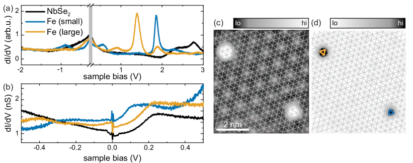
As discussed in the main text, the CDW is incommensurate with the lattice ( Soumyanarayanan et al. (2013)) which implies that the CDW smoothly shifts along the atomic lattice of the surface (see Fig. 1a of the main text and Fig. S11). Hence, the maxima of the CDW can be found at different sites with respect to the atomic lattice. Some striking motifs occur when the CDW maximum coincides with a hollow site (HC) or with a chalcogen site (CC) as illustrated in Fig. 1a of the main manuscript. Interestingly, the configuration with a CDW maximum on a Nb atom (MC) is not observed Gye et al. (2019); Guster et al. (2019). This local configuration is energetically unfavored Gye et al. (2019); Zheng et al. (2018); Guster et al. (2019); Lian et al. (2018); Cossu et al. (2018). To avoid the MC structure smooth grain boundaries are built into the CDW modulation. As illustrated in Fig. S9a,b Fe atoms with small apparent height can be found exactly in the minimum and maximum of the CDW. Hence, this species is assigned to adsorption in the HC position. Consequently, atoms with large apparent height are adsorbed in the MC sites.
S2.4 Determination of Fe-atom adsorption sites relative to the charge-density wave
The adsorption site of Fe atoms relative to the CDW was determined for a set of approximately 90 atoms (used for the data compilation in Fig. 4a of the main manuscript). The center of the Fe atoms as well as the location of the CDW can be determined from the STM images (see superposed CDW grid on the STM topographies in Fig. S10). The error in placing the CDW grids is estimated as , which accounts for the inaccuracy in placing the CDW grid, possible drift effects and for the inaccuracy in finding the center of the atom.
S2.5 Pinning of the charge-density wave
It has been shown that the CDW can be pinned by crystal defects Cossu et al. (2018); Langer et al. (2014); Flicker and van Wezel (2015); Chatterjee et al. (2015); Arguello et al. (2014). Therefore, the phase of the CDW is dictated by the complex interplay of lattice defects and long-range order of the CDW. One such example of a local modification of the CDW in the presence of a defect can be seen in Fig. S11a in the bottom left, where the CC structure of the CDW is pinned around a defect (visible as depression). Hence, one may argue that the Fe atoms can affect the CDW. However, a pinning of the CDW by the adatoms is not observed in the experiment. The adatoms seem not to favor a specific CDW domain as can be seen in Fig. S11a and b. Here, pure HC and CC domains are marked. The adatoms are located in the smooth transition region.
S2.6 Spatial variation of spectra
Figure S12 shows false-color plots of the spectra taken along high-symmetry directions of the YSR patterns across atoms I and IV of the main text. The YSR states exhibit long-range intensity oscillations with no detectable variations in energy within our experimental resolution.
We note that in close vicinity to the atom (Figure S13), the intensity variations are particularly strong and some YSR states are accompanied by a negative value of the differential conductance (NDC) at their high-bias flank. The NDC results from the convolution of YSR states with the tip density of states and can lead to a strong suppression of conductance. In an extreme case, an additional (weak) YSR resonance may be hidden in this part of the spectrum. Examples, where YSR resonances are suppressed below zero are shown by arrows for atom IV, V and VI in Fig. S13. The local variation of the NDC also affects the spatial appearance of the YSR states in the maps as is discussed in the following section.
S2.7 Additional maps of YSR resonances (both bias polarities and thermal excitations)
Figure S14 shows the complete set of the maps of atoms I-VI (the positive bias voltage was presented in the main manuscript). maps at negative bias polarity are depicted in the lower two rows. Opposite bias polarities image the and components of the YSR states, respectively Rusinov (1969).
As expected, the and components lead to distinct scattering patterns. As discussed above, the convolution of tip and sample density of states may lead to distortions of the intensity of individual YSR states, culminating in their suppression in the NDC region of a nearby state. Consequently, also the maps at the energy of a specific YSR state may be affected by a close-lying YSR state.
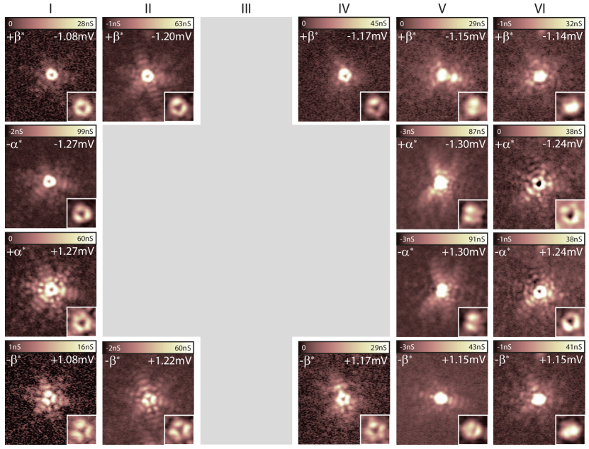
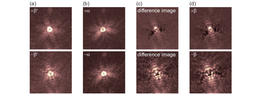
In particular, the -states of atom II, IV and V are affected by the NDC of the -resonances, which are close in energy (Fig. S14). One trick to determine and eliminate the effect of NDC is to investigate the maps of thermally excited YSR states. Thermal excitation of quasiparticles leads to additional resonances within the energy gap of the tip (cf. grey shaded area in Fig. 2b,c in the main text). Whereas the original resonances are found at a bias of , the thermally excited states are found at Ruby et al. (2015a). The thermally excited YSR states are of much less intensity and, therefore, exhibit a small or negligible region of NDC. Figure S15 shows the maps recorded at the corresponding voltages of the thermally excited YSR states for atoms I-VI. In these maps the similarity of the states of atoms I, II and IV is more striking than in the original maps of . To illustrate the impact of the NDC from the -YSR resonances on the state, we simulate the map of by subtracting a fraction of the maps (mimicking the NDC) from the maps. The result is compared to the maps at the energies corresponding to (Fig. S16) and shows remarkable similarity, illustrating the impact of NDC.
S2.8 Determination of YSR energies
To determine the YSR energies, we fit the deconvolved spectra (cf. Fig. S6) in the low-energy region with a set of 4 Gaussians (2 pairs of peaks):
| (S22) |
Here, is an offset, and are the YSR energies, and are four amplitudes and is the width of the Gaussian peaks.
The top panel of Fig. S17c shows the extracted energies of the YSR states of approximately 90 atoms with respect to their location relative to the CDW. The error bar in x-direction results from the inaccuracy in finding the exact position relative to the CDW as discussed along with Fig. S10. The error margins of the YSR energy include the uncertainty in the exact value of the tip’s energy gap , the lock-in modulation of the bias voltage and the standard deviation of the fit routine. Additionally, an error of was added to the energy uncertainty if the peaks are not well separated (i.e. ). This is mainly the case for atoms close to the CDW minimum, where we cannot distinguish the - and -resonances as they are both very close to zero energy (e.g. atom III in the main text). Some of these atoms can be fitted with only one pair of Gauss peaks as the YSR states overlap. In this case both energies have the same value ().
As discussed in the main manuscript, we find a correlation of the YSR energy with position along the CDW symmetry axis. and are largest at the maximum of the CDW and decrease with distance from the maximum. By default, the fit outputs for and are positive. Assuming that and should follow a similar trend, we suggest that the -resonance crosses zero energy, i.e. undergoes the quantum phase transition Franke et al. (2011). Therefore, was assumed for the atoms in close vicinity to the CDW minimum (cf. atom III, the set of atoms with is marked in orange and grey). Having passed the minimum (cf. atom IV) the - and -states can be separated and identified again in the maps (see Fig. 3 in the main manuscript and Figs. S14, S15, S16), i.e. .
The top panel of Fig. 4a in the main manuscript is obtained from the data in Fig. S17c by averaging over all atoms that are found within an interval of a. This corresponds to the uncertainty in the determination of the atoms’ position with respect to the CDW (see above). The error margins in energy are the standard deviations of the averaging including the average of the errors shown in Fig. S17c.
As seen in Fig. S17 and Fig. 4 of the main text, some regions along the CDW cannot be probed by Fe adatoms (grey areas). To understand the absence of data in these regions, we illustrate the phase change of the CDW (black rhombi) with respect to the atomic lattice (grey lattice) along the main symmetry axis in detail in Fig. S18. A HC adsorption site of an Fe atom is marked by a colored triangle on the atomic lattice. The green triangles indicate observed lattice sites, whereas the red triangles indicate that we did not find these adsorption sites relative to the CDW. The latter cases correspond to configurations, where the maximum of the CDW is located on top of a Nb atom. These so-called MC configurations are energetically disfavored as shown by DFT calculations and do not occur on the surface Gye et al. (2019); Zheng et al. (2018); Guster et al. (2019); Lian et al. (2018); Cossu et al. (2018). Hence, the corresponding Fe adsorption sites cannot be found either. This explains the absence of data points in the grey areas with only one exception. The third high symmetry position, where an atomic HC adsorption site would sit exactly in the local minimum of the CDW (marked with the red arrow in Fig. S18b), was also not found in experiment. We may speculate that the energy landscape of the CDW can be affected by the Fe adatoms for this specific adsorption site.
References
- Grüner (1994) G. Grüner, Density waves in solids (CRC Press, 1994).
- Smith et al. (1985) N. V. Smith, S. D. Kevan, and F. J. DiSalvo, J. Phys. C: Solid State Phys. 18, 3175 (1985).
- Rossnagel et al. (2005) K. Rossnagel, E. Rotenberg, H. Koh, N. V. Smith, and L. Kipp, Phys. Rev. B 72, 121103 (2005).
- Inosov et al. (2008) D. S. Inosov, V. B. Zabolotnyy, D. V. Evtushinsky, A. A. Kordyuk, B. Büchner, R. Follath, H. Berger, and S. V. Borisenko, New J. Phys. 10, 125027 (2008).
- Inosov et al. (2009) D. S. Inosov, D. V. Evtushinsky, V. B. Zabolotnyy, A. A. Kordyuk, B. Büchner, R. Follath, H. Berger, and S. V. Borisenko, Phys. Rev. B 79, 125112 (2009).
- Rahn et al. (2012) D. J. Rahn, S. Hellmann, M. Kalläne, C. Sohrt, T. K. Kim, L. Kipp, and K. Rossnagel, Phys. Rev. B 85, 224532 (2012).
- Ménard et al. (2015) G. C. Ménard, S. Guissart, C. Brun, S. Pons, V. S. Stolyarov, F. Debontridder, M. V. Leclerc, E. Janod, L. Cario, D. Roditchev, P. Simon, and T. Cren, Nature Phys. 11, 1013 (2015).
- Bawden et al. (2016) L. Bawden, S. P. Cooil, F. Mazzola, J. M. Riley, L. J. Collins-McIntyre, V. Sunko, K. W. B. Hunvik, M. Leandersson, C. M. Polley, T. Balasubramanian, T. K. Kim, M. Hoesch, J. W. Wells, G. Balakrishnan, M. S. Bahramy, and P. D. C. King, Nature Comm. 7, 11711 (2016).
- Xi et al. (2016) X. Xi, Z. Wang, W. Zhao, J.-H. Park, K. T. Law, H. Berger, L. Forró, J. Shan, and K. F. Mak, Nature Phys. 12, 139 (2016).
- Hewson (1993) A. C. Hewson, The Kondo Problem to Heavy Fermions (Cambridge University Press, 1993).
- Yu (1965) L. Yu, Acta Phys. Sin. 21, 75 (1965).
- Shiba (1968a) H. Shiba, Prog. Theor. Phys. 40, 435 (1968a).
- Rusinov (1969) A. I. Rusinov, JETP Lett. 9, 85 (1969).
- Moca et al. (2008) C. P. Moca, E. Demler, B. Jankó, and G. Zaránd, Phys. Rev. B 77, 174516 (2008).
- Kirs̆anskas et al. (2015) G. Kirs̆anskas, M. Goldstein, K. Flensberg, L. I. Glazman, and J. Paaske, Phys. Rev. B 92, 235422 (2015).
- Shiba (1968b) H. Shiba, Prog. Theor. Phys. 40, 435 (1968b).
- Ruby et al. (2015a) M. Ruby, F. Pientka, Y. Peng, F. von Oppen, B. W. Heinrich, and K. J. Franke, Phys. Rev. Lett. 115, 087001 (2015a).
- Tersoff and Hamann (1985) J. Tersoff and D. R. Hamann, Phys. Rev. B 31, 805 (1985).
- Ruby et al. (2015b) M. Ruby, B. W. Heinrich, J. I. Pascual, and K. J. Franke, Phys. Rev. Lett. 114, 157001 (2015b).
- Choi et al. (2017) D.-J. Choi, C. Rubio-Verdú, J. De Bruijckere, M. M. Ugeda, N. Lorente, and J. I. Pascual, Nature Commun. 8, 15175 (2017).
- Soumyanarayanan et al. (2013) A. Soumyanarayanan, M. M. Yee, Y. He, J. van Wezel, D. J. Rahn, K. Rossnagel, E. W. Hudson, M. R. Norman, and J. E. Hoffman, Proc. Natl. Acad. Sci. 110, 1623 (2013).
- Gye et al. (2019) G. Gye, E. Oh, and H. W. Yeom, Phys. Rev. Lett. 122, 016403 (2019).
- Guster et al. (2019) B. Guster, C. Rubio-Verdú, R. Robles, J. Zaldívar, P. Dreher, M. Pruneda, J. Á. Silva-Guillén, D.-J. Choi, J. I. Pascual, M. M. Ugeda, P. Ordejón, and E. Canadell, Nano Lett. 19, 3027 (2019).
- Zheng et al. (2018) F. Zheng, Z. Zhou, X. Liu, and J. Feng, Phys. Rev. B 97, 081101 (2018).
- Lian et al. (2018) C. S. Lian, C. Si, and W. Duan, Nano Letters 18, 2924 (2018).
- Cossu et al. (2018) F. Cossu, A. G. Moghaddam, K. Kim, H. A. Tahini, I. Di Marco, H.-W. Yeom, and A. Akbari, Phys. Rev. B 98, 195419 (2018).
- Langer et al. (2014) M. Langer, M. Kisiel, R. Pawlak, F. Pellegrini, G. E. Santoro, R. Buzio, A. Gerbi, G. Balakrishnan, A. Baratoff, E. Tosatti, and E. Meyer, Nat. Mater. 13, 173 (2014).
- Flicker and van Wezel (2015) F. Flicker and J. van Wezel, Nature Commun. 6, 7034 (2015).
- Chatterjee et al. (2015) U. Chatterjee, J. Zhao, M. Iavarone, R. Di Capua, J. P. Castellan, G. Karapetrov, C. D. Malliakas, M. G. Kanatzidis, H. Claus, J. P. C. Ruff, F. Weber, J. Van Wezel, J. C. Campuzano, R. Osborn, M. Randeria, N. Trivedi, M. R. Norman, and S. Rosenkranz, Nat. Commun. 6, 6313 (2015).
- Arguello et al. (2014) C. J. Arguello, S. P. Chockalingam, E. P. Rosenthal, L. Zhao, C. Gutiérrez, J. H. Kang, W. C. Chung, R. M. Fernandes, S. Jia, A. J. Millis, R. J. Cava, and A. N. Pasupathy, Phys. Rev. B 89, 235115 (2014).
- Franke et al. (2011) K. J. Franke, G. Schulze, and J. I. Pascual, Science 332, 940 (2011).